

SGS Thomson Microelectronics M74HC648, M74HC646 Datasheet
M74HC646
M74HC648
HC6 46 OCTA L BUSTRAN S CE I VER / REG I STE R (3-STAT E)
HC648 OCTAL BUS TRANSCEIVER/REGISTER (3-STATE, INV.)
.HIGH SPEED
f
= 73 MHz(TYP.) AT VCC=5V
MAX
.LOWPOWERDISSIPATION
ICC=4µA(MAX.) AT TA=25°C
.HIGH NOISEIMMUNITY
V
NIH=VNIL
.OUTPUT DRIVE CAPABILITY
15 LSTTL LOADS
=28%VCC(MIN.)
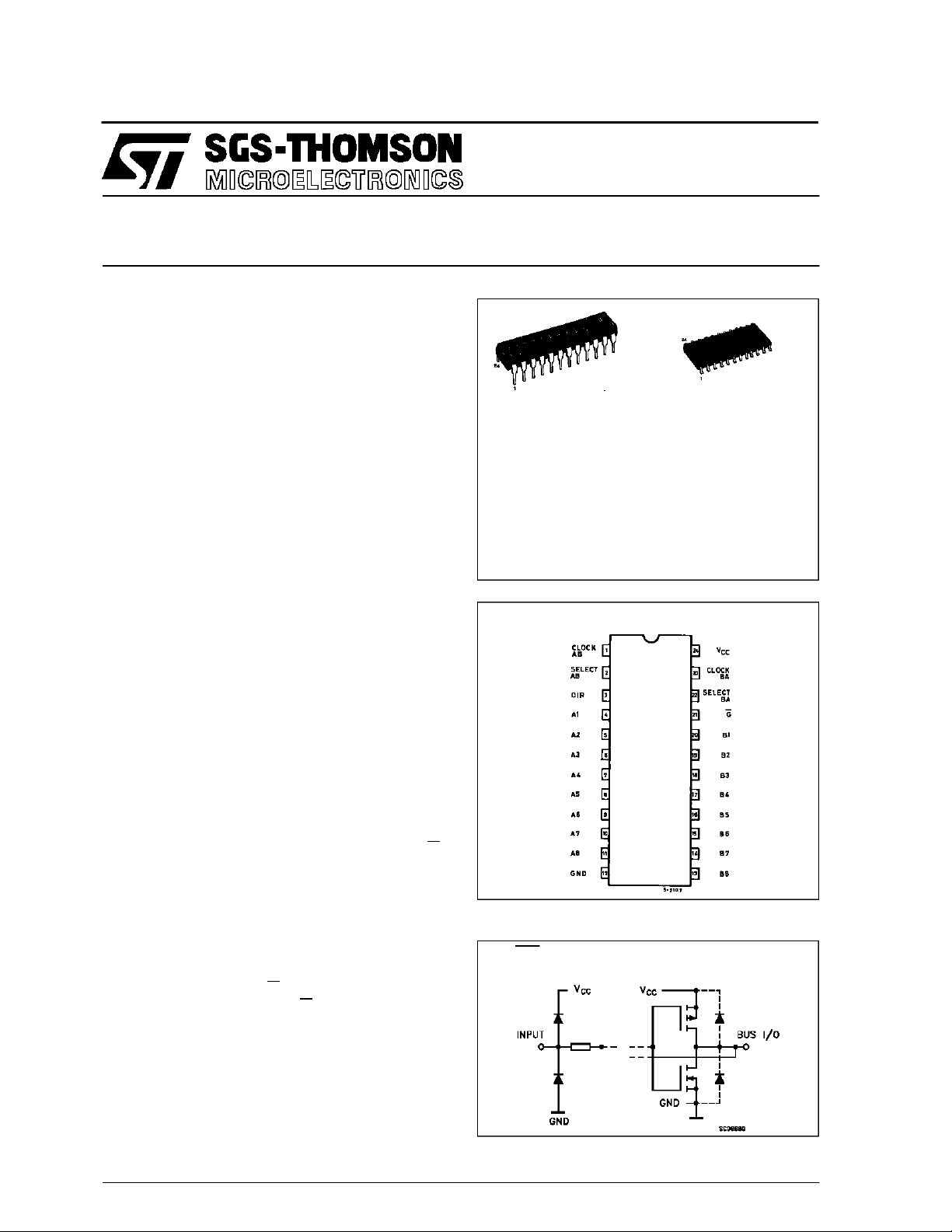
B1R
(PlasticPackage)
M1R
(MicroPackage)
.SYMMETRICALOUTPUT IMPEDANCE
IOH=IOL=6 mA(MIN.)
.BALANCEDPROPAGATION DELAYS
t
PLH=tPHL
.WIDE OPERATINGVOLTAGE RANGE
VCC(OPR)= 2 V TO6 V
M74HC X XXM1R M74H CXXXB1 R
ORDER CODES :
.PIN ANDFUNCTION COMPATIBLE
WITH 54/74LS646/648
DESCRIPTION
The M74HC646/648 are highspeedCMOSOCTAL
BUS TRANSCEIVERS AND REGISTERS, (3STATE) fabricated in silicon gate C2MOS technology. They have the same high speedperformance
ofLSTTLcombined withtrueCMOS low powerconsumption.
These devices consist of bus transceiver circuits
with3-state output, D-typeflip-flops,and controlcircuitryarranged for multiplexed transmission ofdata
directly from the inputbus or from the internal registers.Dataon theAor Bbuswill beclocked intothe
registers on the low-to-high transition of the appropriate clockpin(ClockAB- orClockBA).Enable(G)
and direction (DIR) pins are provided to control the
transceiverfunctions. In thetransceiver mode, data
present at the high-impedance port may be stored
in either register or in both.
The select controls (Select AB select BA) canmultiplex stored and real-time (transparent mode) data.
The direction control determines which bus will receivedata whenenable G is active(low).
In theisolation mode (enable G high),”A” data may
be stored in one register and/or ”B” data may be
storedinthe otherregister.Whenanoutputfunction
is disabled, the input function is still enabled and
may be used to store and transmit data. Only one
of the two buses, A or B, may be driven at a time.
All inputs are equipped with protection circuits
PIN CONNECTIONS (top view)
INPUT AND OUTPUT EQUIVALENT CIRCUIT
GAB,GAB,CAB, A, B
SAB,SBA, CBA
October 1993
1/12
M74HC646/648
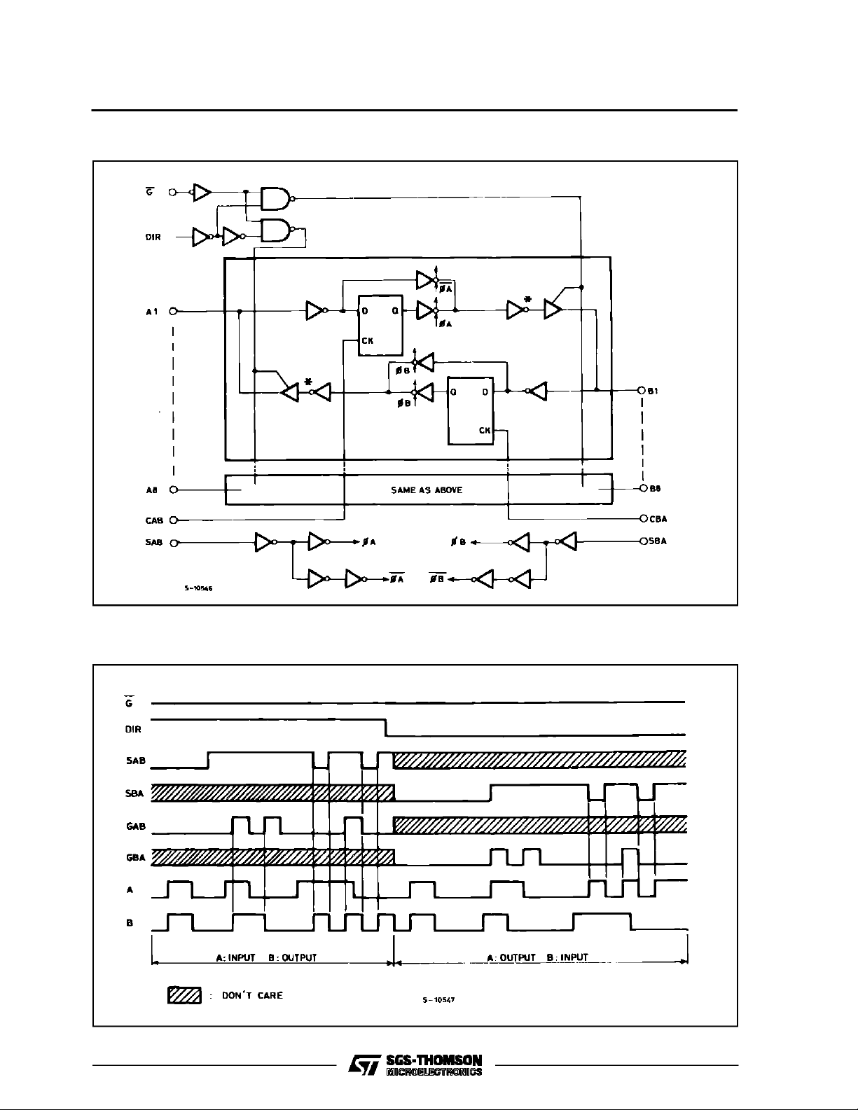
LOGIC DIAGRAM (HC648)
Note: In case ofM54/74HC646 output invertermarked *at A bus and B bus are eliminated.
TIMING CHART
2/12
M74HC646/648
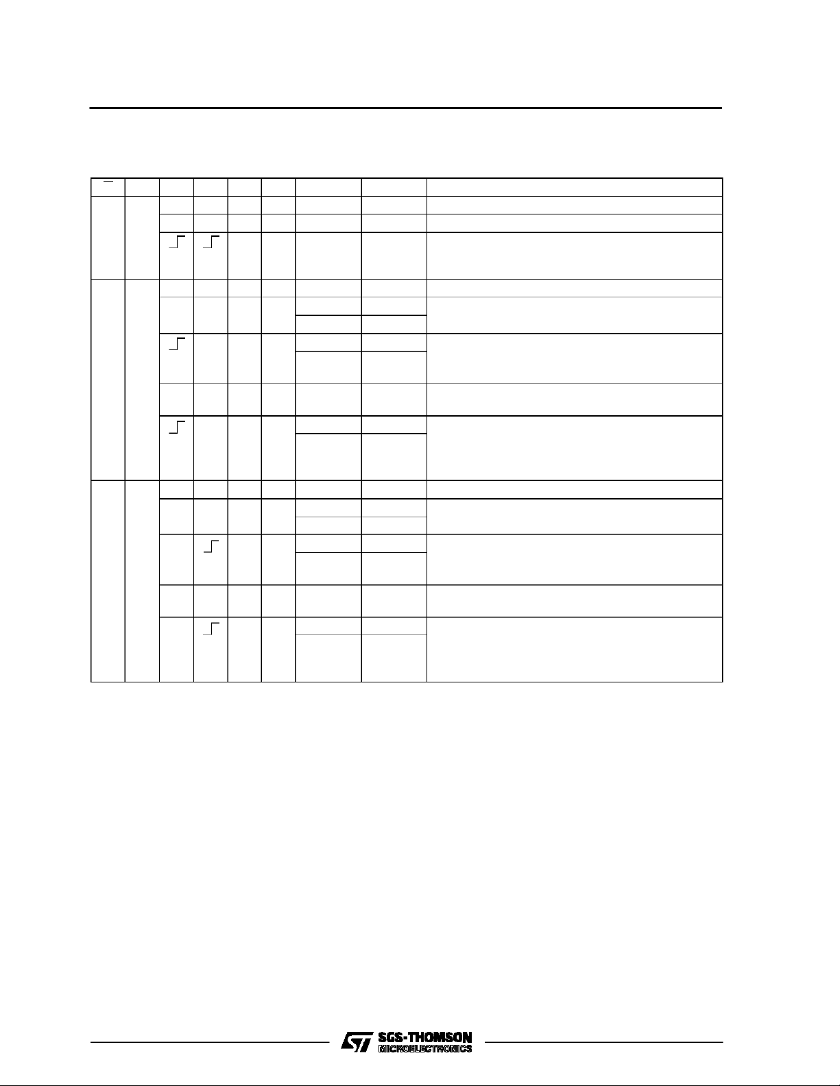
TRUTH TABLE
HC646 ( The truth table for HC648 is the same as this, but with the outputs inverted)
G DIR CAB CBA SAB SBA A B FUNCTION
INPUTS INPUTS Both the A bus and the B bus are inputs
HX
LH
LL
X : DON’TCARE
Z :HIGH IMPEDANCE
Qn :THE DATA STOREDTO THEINTERNALFLIP-FLOPSBY MOST RECENTLOW TO HIGHTRANSITION OF THECLOCK INPUTS
* : THEDATA AT THE A ANDB BUSWILLBE STORED TO THE INTERNALFLIP-FLOPS ON EVERY LOWTO HIGH TRANSITIONOF
THECLOCK INPUTS
X X X X Z Z The output functions of the A and B bus are disabled
X X INPUTS INPUTS Both the A and B bus are used for inputs to the
internal flip-flops. Data at the bus will be stored on
low to high transition of the clock inputs
INPUTS OUTPUTS The A bus are inputs and the B bus are outputs
X X* L X L L The data at the A bus are displayed at the B bus
HH
X* L X L L The data at the A bus are displayed at the B bus.
HH
The data of the A bus are stored to the internal
flip-flop on low to high transition of th clock pulse.
X X* H X X Qn The data stored to the internal flip-flop are dispayed
at the B bus
X* H X L L The data at the A bus are stored to the internal flip-
HH
flop on low to high transition of the clock pulse. The
states of the internal flip-flops output directly to the
B bus
OUTPUTS INPUTS The B bus are inputs and the A bus are outputs
X* X X L
L L The data at the B bus are displayed at the A bus
HH
X* X L L L The data at the B bus are displayed at the A bus.
HH
The data of the B bus are stored to the internal flipflop on low to high transition of the clock pulse
X* X X H Qn X The data stored to the internal flip-flops are
displayed at the A bus
x* X H L L the data at the B bus are stored to the internal flip-
HH
flop on low to high transition of the clock pulse. The
states of the internal flip-flops output directly to the
A bus
3/12
M74HC646/648
PIN DESCRIPTION
PIN No SYMBOL NAME AND FUNCTION
1 CLOCK AB A to B Clock Input (LOW to HIGH, Edge-Trigged)
2 SELECT AB Select A to B Source Input
3 GAB Direction Control Input
4, 5, 6, 7, 8, 9, 10, 11 A1 to A8 A data Inputs/Outputs
20, 19, 18, 17, 16, 15, 14, 13 B1 to B8 B Data Inputs/Outputs
21 G Output Enable Input (Active LOW)
22 SELECT BA Select B to A Source Input
23 CLOCK BA B to A Clock Input (LOW to HIGH, Edge-Triggered)
12 GND Ground (0V)
24 V
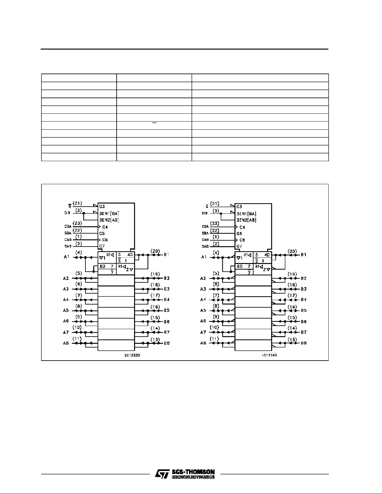
IEC LOGIC SYMBOLS
CC
HC646 HC648
Positive Supply Voltage
4/12
 Loading...