

M54/74HC620
M54/74HC623
OCTAL BUS TRANSCEIVER
HC620 3 STATE INVERTIN G HC623 3 STATENON INVE RTING
.HIGH SPEED
tPD= 10 ns(TYP.) AT VCC=5V
.LOWPOWERDISSIPATION
ICC=4µA(MAX.) AT TA=25°C
.HIGH NOISEIMMUNITY
V
NIH=VNIL
.OUTPUT DRIVE CAPABILITY
15 LSTTL LOADS
=28%VCC(MIN.)
B1R
(PlasticPackage)
F1R
(CeramicPackage)
.SYMMETRICALOUTPUT IMPEDANCE
|IOH|=IOL=6 mA(MIN.)
.BALANCEDPROPAGATION DELAYS
t
PLH=tPHL
.WIDE OPERATINGVOLTAGE RANGE
VCC(OPR)= 2V to 6V
.PIN ANDFUNCTION COMPATIBLE
WITH LS620/623
M1R
(MicroPackage)
ORDER CODES :
M54HC X XXF1R M74H CXXXM1R
M74HC X XXB1R M74HCX X XC1R
C1R
(Chip Carrier)
DESCRIPTION
The M54/74HC620/623 are high speed CMOS
OCTALBUS TRANSCEIVERS fabricated in silicon
gate C2MOS technology. They havethe same high
speed performance of LSTTL combined with true
CMOS low powerconsumption.
Theseoctalbus transceiversare designed forasynchronous two-way communication between data
buses. The control function implementation allows
maximumflexibility in timing.
These devices allow data transmission from the A
bus to Bbus or from the B to the A bus depending
upon the logiclevelsat theenable inputs (GBAand
GAB).The enable inputs canbe used to disable the
deviceso that the busesare effectivelyisolated.
The dual-enable configuration gives these devices
thecapabilitytostoredataby simultaneousenabling
of GBA andGAB.
Each output reinforces its input in this transceiver
configuration. Thus, when both control inputs are
enabled and all otherdata sources to the two sets
of bus lines areathigh impedance, both setsof bus
lines(16 in all) willremain attheir laststates. The 8bit codesappearing onthe twosets of buses will be
identical for the ’HC623 or complementary for the
’HC620. Allinputsare equipped with protection circuits against static discharge and transient excess
voltage.
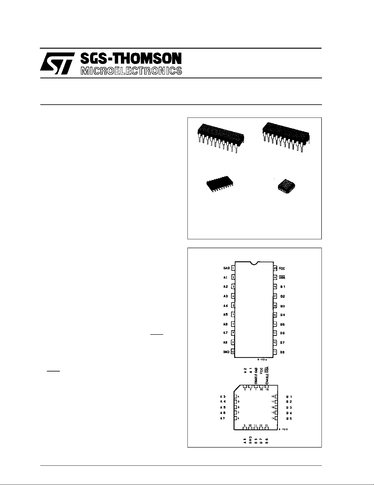
PIN CONNECTIONS(top view)
NC =
No Internal
Connection
October 1992
1/11
M54/M74HC620/623
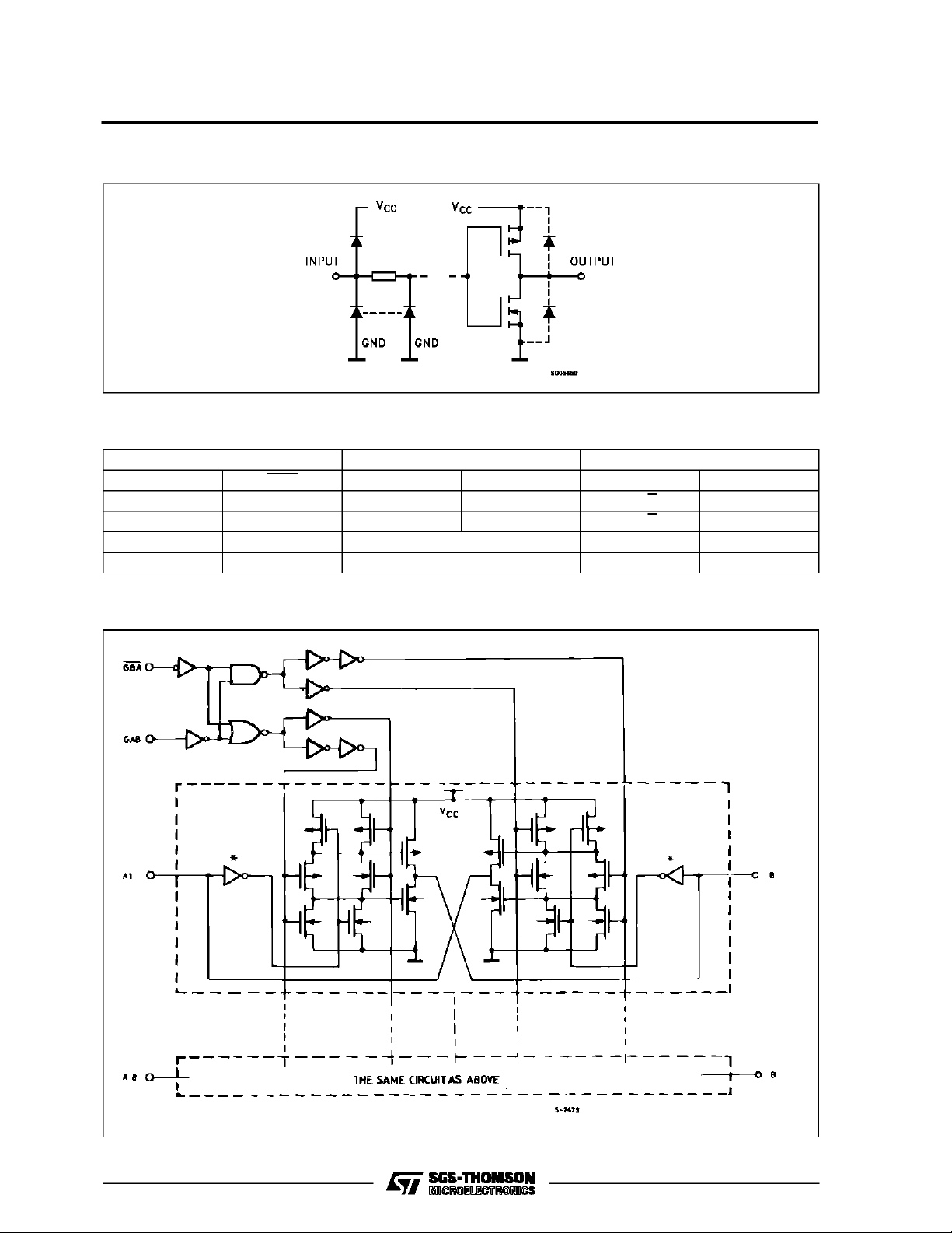
INPUT AND OUTPUT EQUIVALENT CIRCUIT
TRUTH TABLE
INPUTS FUNCTION OUTPUS
GAB GBA A Bus B Bus HC620 HC623
L L Output Input A = B A = B
H H Input Output B = A B = A
L H High Impedance Z Z
H L High Impedance Z Z
LOGI C DI AG RAM
2/11
PIN DESC RIPTION
PIN No SYMBOL NAME AND FUNCTION
1, 19 GBA , GAB Direction Controls
2, 3, 4, 5, 6, 7, 8, 9 A1 to A8 Data Inputs/Outputs
11, 12, 13, 14, 15, 16, 17, 18 B1 to B8 Data Inputs/Outputs
10 GND Ground (0V)
20 V
CC
Positive Supply Voltage
IEC LOGIC SYMBOLS
HC620 HC6 23
M54/M74HC620/623
ABSOLU TE M AXIMU M R AT ING S
Symbol Parameter Value Unit
V
CC
V
V
O
I
IK
I
OK
I
O
I
or I
CC
P
D
T
stg
T
AbsoluteMaximumRatingsarethose values beyondwhichdamage tothedevicemayoccur. Functionaloperationunder these conditionisnotimplied.
(*)500 mW: ≅ 65oC derateto300 mWby 10mW/oC: 65oCto85oC
Supply Voltage -0.5 to +7 V
DC Input Voltage -0.5 to VCC+ 0.5 V
I
DC Output Voltage -0.5 to VCC+ 0.5 V
DC Input Diode Current ± 20 mA
DC Output Diode Current ± 20 mA
DC Output Source Sink Current Per Output Pin ± 35 mA
DC VCCor Ground Current ± 70 mA
GND
Power Dissipation 500 (*) mW
Storage Temperature -65 to +150
Lead Temperature (10sec) 300
L
o
C
o
C
3/11
M54/M74HC620/623
RECO MM ENDED OPERAT I N G CONDITI O NS
Symbol Parameter Value Unit
V
V
V
T
t
r,tf
DC SPECIFICATIONS
Symbol Parameter
V
IH
V
V
OH
V
OL
I
I
OZ
I
CC
Supply Voltage 2 to 6 V
CC
Input Voltage 0 to V
I
Output Voltage 0 to V
O
Operating Temperature: M54HC Series
op
M74HC Series
CC
CC
-55 to +125
-40 to +85
Input Rise and Fall Time VCC= 2 V 0 to 1000 ns
V
= 4.5 V 0 to 500
CC
V
= 6 V 0 to 400
CC
Test Conditions Value
V
(V)
CC
=25oC
T
A
54HC and 74HC
-40 to 85oC
74HC
-55 to 125oC
Min. Typ. Max. Min. Max. Min. Max.
High Level Input
Voltage
2.0 1.5 1.5 1.5
4.5 3.15 3.15 3.15
6.0 4.2 4.2 4.2
Low Level Input
IL
Voltage
2.0 0.5 0.5 0.5
4.5 1.35 1.35 1.35
6.0 1.8 1.8 1.8
High Level
Output Voltage
Low Level Output
Voltage
Input Leakage
I
Current
3 State Output
Off State Current
Quiescent Supply
2.0
V
=
I
4.5 4.4 4.5 4.4 4.4
6.0 5.9 6.0 5.9 5.9
4.5 I
6.0 I
2.0
4.5 0.0 0.1 0.1 0.1
6.0 0.0 0.1 0.1 0.1
4.5 I
6.0 I
6.0
6.0
IO=-20 µA
V
IH
or
V
IL
=-6.0 mA 4.18 4.31 4.13 4.10
O
=-7.8 mA 5.68 5.8 5.63 5.60
O
V
=
I
IO=20µA
V
IH
or
V
IL
= 6.0 mA 0.17 0.26 0.33 0.40
O
= 7.8 mA 0.18 0.26 0.33 0.40
O
VI=VCCor GND ±0.1 ±1 ±1 µA
VI=VIHor V
VO=VCCor GND
1.9 2.0 1.9 1.9
0.0 0.1 0.1 0.1
IL
±0.5 ±5 ±10 µA
6.0 VI=VCCor GND 4 40 80 µA
Current
54HC
V
V
o
C
o
C
Unit
V
V
V
V
4/11

M54/M74HC620/623
AC ELECTRICAL CHARACTERISTICS (CL=50pF,Inputtr=tf=6ns)
Test Conditions Value
T
=25oC
Symbol Parameter
t
t
TLH
THL
Output Transition
Time
V
C
CC
(V)
L
(pF)
2.0
50
4.5 7121518
A
54HC and 74HC
Min. Typ. Max. Min. Max. Min. Max.
25 60 75 90
6.0 6101315
t
PLH
t
PHL
Propagation
Delay Time
(for HC620)
2.0
50
4.5 12 20 25 30
41 100 125 150
6.0 10 17 21 26
2.0
150
4.5 16 26 33 39
55 130 165 195
6.0 14 22 28 33
t
t
PLH
PHL
Propagation
Delay Time
(for HC623)
2.0
50
4.5 12 17 21 26
38 85 105 130
6.0 10 14 18 22
2.0
150
4.5 16 26 33 39
51 130 165 195
6.0 14 22 28 33
t
t
PZL
PZH
Output Enable
Time
2.0
50 RL=1KΩ
4.5 19 30 38 45
57 150 190 225
6.0 16 26 32 38
2.0
150 R
4.5 23 36 45 54
=1KΩ
L
69 180 225 270
0 20313846
t
PLZ
t
PHZ
Output Disable
Time
2.0
50 R
4.5 18 25 31 38
=1KΩ
L
43 125 155 190
6.0 15 21 26 32
C
C
PD
CPDisdefined as thevalueofthe IC’s internal equivalent capacitance which iscalculatedfrom theoperating current consumption without load.(Refer
to TestCircuit).Averageoperting current canbe obtained by the followingequation. ICC(opr) = CPD•VCC•fIN+I
Input Capacitance 5 10 10 10 pF
IN
(*) Power Dissipation
Capacitance
for HC620
for HC623
32
34
-40 to 85oC
74HC
CC
-55 to 125oC
54HC
Unit
ns
ns
ns
ns
ns
ns
ns
ns
pF
5/11

M54/M74HC620/623
SWITCHING CHARACTERISTICS TEST WAVEFORM
TEST CIRCUIT ICC(Opr.) CPDCALCULATION
V
GND
CC
INPUT WAVEFORMIS THE SAME AS THAT IN CASE OF
SWITCHINGCHARACTERISTICSTEST.
CPDisto becalculated withthe following formula
byusing the measured value of ICC(Opr.)in the
testcircuit opposite.
I
(
Opr
CPD=
CC
fINxV
.)
CC
In determining the typical value of CPD, a relativelyhigh frequency of 1MHzwasapplied tofIN,
in order to eliminate any error caused by the
quiescentsupply current.
6/11

Plastic DIP20 (0.25) MECHANICAL DATA
M54/M74HC620/623
DIM.
MIN. TYP. MAX. MIN. TYP. MAX.
a1 0.254 0.010
B 1.39 1.65 0.055 0.065
b 0.45 0.018
b1 0.25 0.010
D 25.4 1.000
E 8.5 0.335
e 2.54 0.100
e3 22.86 0.900
F 7.1 0.280
I 3.93 0.155
L 3.3 0.130
Z 1.34 0.053
mm inch
P001J
7/11

M54/M74HC620/623
Ceramic DIP20 MECHANICAL DATA
DIM.
MIN. TYP. MAX. MIN. TYP. MAX.
A 25 0.984
B 7.8 0.307
D 3.3 0.130
E 0.5 1.78 0.020 0.070
e3 22.86 0.900
F 2.29 2.79 0.090 0.110
G 0.4 0.55 0.016 0.022
I 1.27 1.52 0.050 0.060
L 0.22 0.31 0.009 0.012
M 0.51 1.27 0.020 0.050
N1 4° (min.), 15° (max.)
P 7.9 8.13 0.311 0.320
Q 5.71 0.225
mm inch
8/11
P057H

SO20 MECHANICAL DATA
M54/M74HC620/623
DIM.
MIN. TYP. MAX. MIN. TYP. MAX.
A 2.65 0.104
a1 0.10 0.20 0.004 0.007
a2 2.45 0.096
b 0.35 0.49 0.013 0.019
b1 0.23 0.32 0.009 0.012
C 0.50 0.020
c1 45° (typ.)
D 12.60 13.00 0.496 0.512
E 10.00 10.65 0.393 0.419
e 1.27 0.050
e3 11.43 0.450
F 7.40 7.60 0.291 0.299
L 0.50 1.27 0.19 0.050
M 0.75 0.029
S8°(max.)
mm inch
P013L
9/11

M54/M74HC620/623
PLCC20 MECHANICAL DATA
DIM.
MIN. TYP. MAX. MIN. TYP. MAX.
A 9.78 10.03 0.385 0.395
B 8.89 9.04 0.350 0.356
D 4.2 4.57 0.165 0.180
d1 2.54 0.100
d2 0.56 0.022
E 7.37 8.38 0.290 0.330
e 1.27 0.050
e3 5.08 0.200
F 0.38 0.015
G 0.101 0.004
M 1.27 0.050
M1 1.14 0.045
mm inch
10/11
P027A

M54/M74HC620/623
Information furnishedis believed to be accurate and reliable. However, SGS-THOMSON Microelectronicsassumes no responsability for the
consequences of useof suchinformation nor for any infringementof patents or other rightsof third parties which may results from its use. No
license is granted byimplication or otherwiseunder any patentor patentrights ofSGS-THOMSON Microelectronics. Specificationsmentioned
in thispublication are subjectto changewithout notice. This publicationsupersedes andreplaces all information previouslysupplied.
SGS-THOMSON Microelectronicsproducts are not authorized foruse ascritical componentsinlifesupportdevices orsystemswithoutexpress
written approval of SGS-THOMSON Microelectonics.
1994SGS-THOMSON Microelectronics- All Rights Reserved
Australia -Brazil - France - Germany - Hong Kong - Italy -Japan - Korea -Malaysia - Malta - Morocco - The Netherlands -
Singapore -Spain - Sweden- Switzerland - Taiwan - Thailand - UnitedKingdom - U.S.A
SGS-THOMSON Microelectronics GROUP OFCOMPANIES
11/11
 Loading...