

SGS Thomson Microelectronics M74HC592 Datasheet
.HIGH SPEED
f
= 35 MHz(TYP.) AT VCC=5V
MAX
.LOWPOWERDISSIPATION
ICC=4µA(MAX.) AT TA=25°C
.OUTPUTDRIVE CAPABILITY
10 LSTTL LOADS
.BALANCEDPROPAGATION DELAYS
t
PLH=tPHL
.SYMMETRICALOUTPUT IMPEDANCE
IOL=IOH = 4 mA (MIN.)
.HIGH NOISE IMMUNITY
V
NIH=VNIL
=28%VCC(MIN.)
.WIDE OPERATINGVOLTAGE RANGE
VCC(OPR)= 2V TO6 V
.PIN ANDFUNCTION COMPATIBLE
WITH 54/74LS592
DESCRIPTION
M54HC592
M74HC592
8 BIT REGISTERBINARY COUNTER
B1R
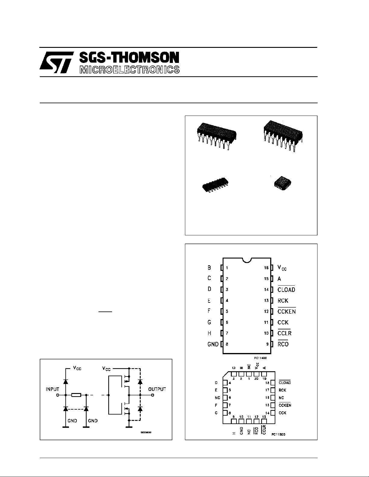
(PlasticPackage)
M1R
(MicroPackage)
ORDER CODES :
M54HC 592F1R M74H C592M1R
M74HC 592B1R M74HC5 92C1R
F1R
(CeramicPackage)
C1R
(Chip Carrier)
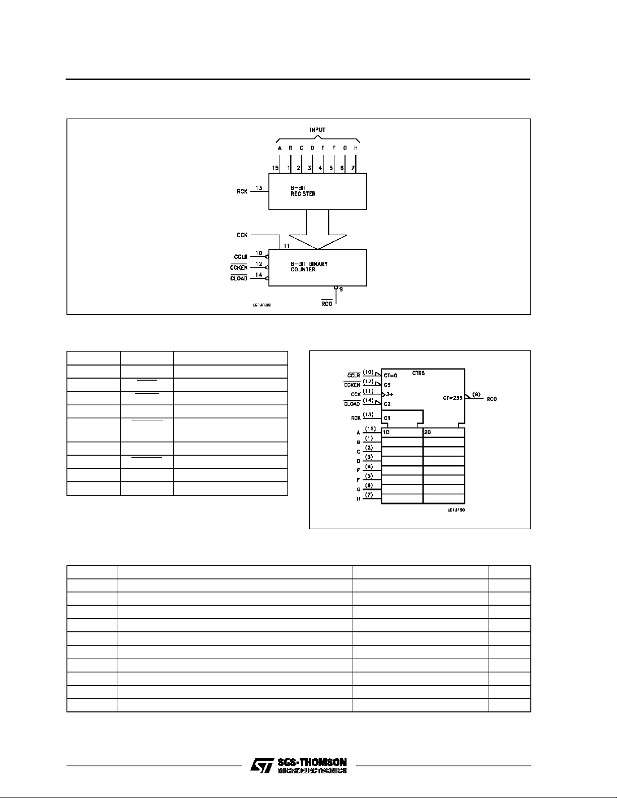
The M54/74HC592 is a high speed CMOS 8 BIT
REGISTER COUNTER fabricated in silicon gate
C2MOStechnology. Ithasthesamehighspeedperformance of LSTTL combined with true CMOS low
powerconsumption.
The M54/74HC592 is a parallelinput, 8 bit storage
register feeding an8bitbinarycounter.Both theregisterandthe counter have individual positiveedge
triggered clock. In addition, the counter has direct
loadandclearfunctions.Expansion iseasily accomplished by connecting RCO af the firststage to the
count enable of the second stage. All inputs are
equipped with protection circuits against static discharge andtransient excess voltage.
INPUT AND OUTPUT EQUIVALENT CIRCUIT
PIN CONNECTIONS(top view)
NC =
No Internal
Connection
October 1993
1/13
M54/M74HC592
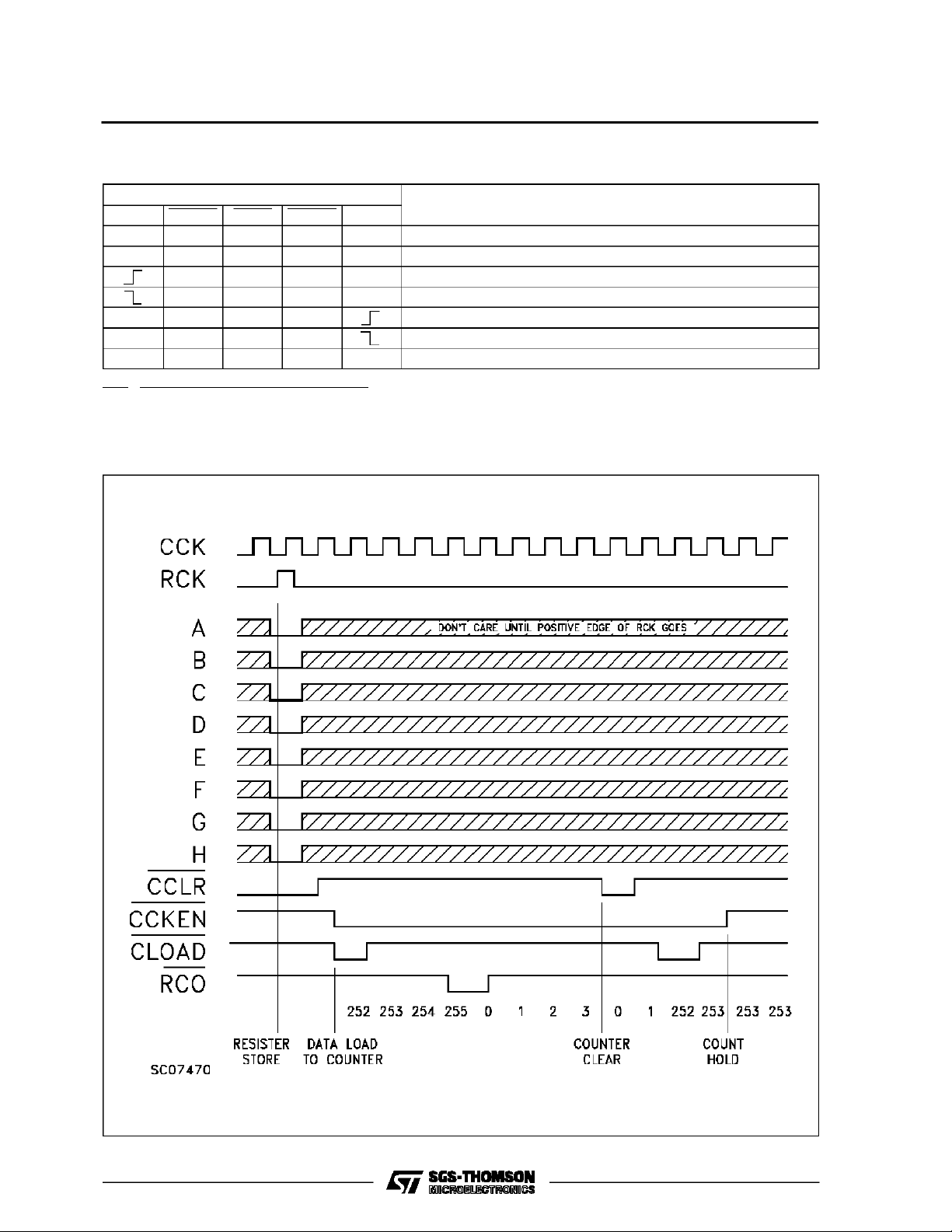
TRUTH TABLE
INPUTS
RCK CLOAD CCLR CCKEN CCK
X L H X X REGISTER DATA IS LOADED INTO COUNTER
X H L X X COUNTER CLEAR
H H X X THE DATA OF A THRU H INPUTS IS STORED INTO REGISTER
H H X X REGISTER STATE IS NOT CHANGED
X H H L COUNTER ADVANCES THE COUNT
X H H L NO COUNT
X H H H X NO COUNT
X:Don’t Care
RCO= QA’• QB’• QC’ • QD’ • QE’• QF’ • QG’• QH’
(QA’toQH’:Internaloutputs of thecounter)
FUNCTION
TIM ING C HAR T
2/13
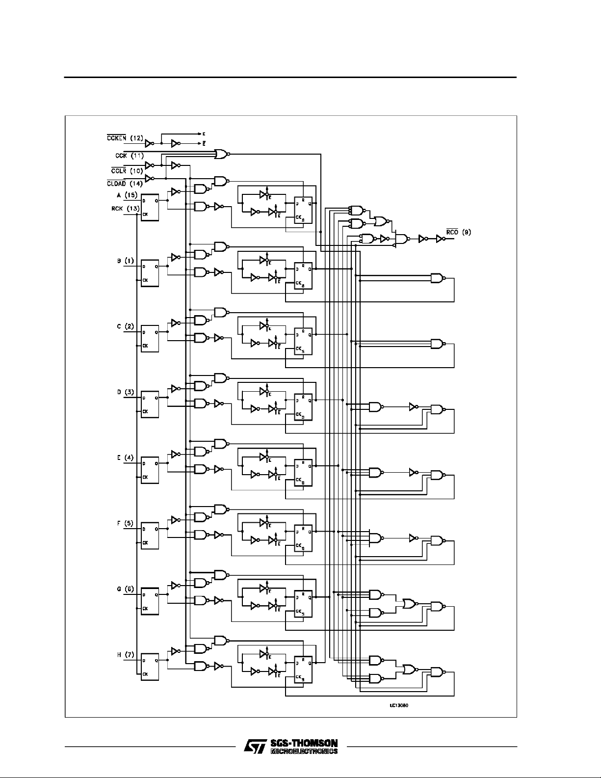
LOGI C DI AGRAM
M54/M74HC592
3/13
M54/M74HC592
BLOCK DIAGRAM
PIN DESC RIPTION
IEC LOGIC SYMBOL
PIN No SYMBOL NAME AND FUNCTION
1 to 7, 15 A to H Data Inputs
9 RCO Ripple Counter Output
10 CCLR Counter Clear Input
11 CCK Counter Clock Input
12 CCKEN Counter Clock Enable
Input
13 RCK Register Clock Input
14 CLOAD Counter Load Input
8 GND Ground (0V)
16 V
CC
Positive Supply Voltage
ABSOLU TE M AXIMU M R AT INGS
Symbol Parameter Value Unit
V
CC
V
V
O
I
IK
I
OK
I
O
or I
I
CC
P
D
T
stg
T
AbsoluteMaximumRatingsarethose valuesbeyond whichdamage to thedevice mayoccur.Functional operation under these conditionisnotimplied.
(*)500 mW: ≅ 65oC derateto300 mWby 10mW/oC: 65oCto85oC
Supply Voltage -0.5 to +7 V
DC Input Voltage -0.5 to VCC+ 0.5 V
I
DC Output Voltage -0.5 to VCC+ 0.5 V
DC Input Diode Current ± 20 mA
DC Output Diode Current ± 20 mA
DC Output Source Sink Current Per Output Pin ± 25 mA
DC VCCor Ground Current ± 50 mA
GND
Power Dissipation 500 (*) mW
Storage Temperature -65 to +150
Lead Temperature (10sec) 300
L
o
C
o
C
4/13
 Loading...