

SGS Thomson Microelectronics M74HC574, M74HC564 Datasheet
OCTAL D-TYPE FLIP FLOP WITH 3 STATE OUTPUT
HC564 INVERTING - HC574 NON INVERTING
.HIGH SPEED
f
= 62MHz (TYP.) AT VCC=5V
MAX
.LOWPOWER DISSIPATION
ICC=4µA(MAX.) AT TA=25°C
.HIGH NOISE IMMUNITY
V
NIH=VNIL
= 28% VCC(MIN)
.OUTPUT DRIVE CAPABILITY
15 LSTTLLOADS
.SYMMETRICAL OUTPUT IMPEDANCE
IOL=IOH= 6 mA (MIN.)
.BALANCEDPROPAGATIONDELAYS
t
PLH=tPHL
.WIDE OPERATINGVOLTAGERANGE
VCC(OPR)= 2 V TO 6 V
.PIN ANDFUNCTION COMPATIBLE
WITH 54/74LS564/574
DESCRIPTION
The M54/74HC564and M54HC574 arehigh speed
CMOSOCTALD-TYPEFLIPFLOPWITH3-STATE
OUTPUTS fabricated with in silicon gate C2MOS
technology. They have the same high speed performance of LSTTL combined with true CMOS low
power comsuption. These8-bit D-type flip-flops are
controlled by aclockinput(CK) and anouputenable
input(OE).On thepositivetransition of theclock,the
Qoutputswillbesettothelogic statethatweresetup
at the D inputs (HC574) or their complements
(HC564).
While the OE input is low, the eight outputs willbe
in a normal logic state(high or low logic level), and
while high level,theoutputs will be in ahigh imped-
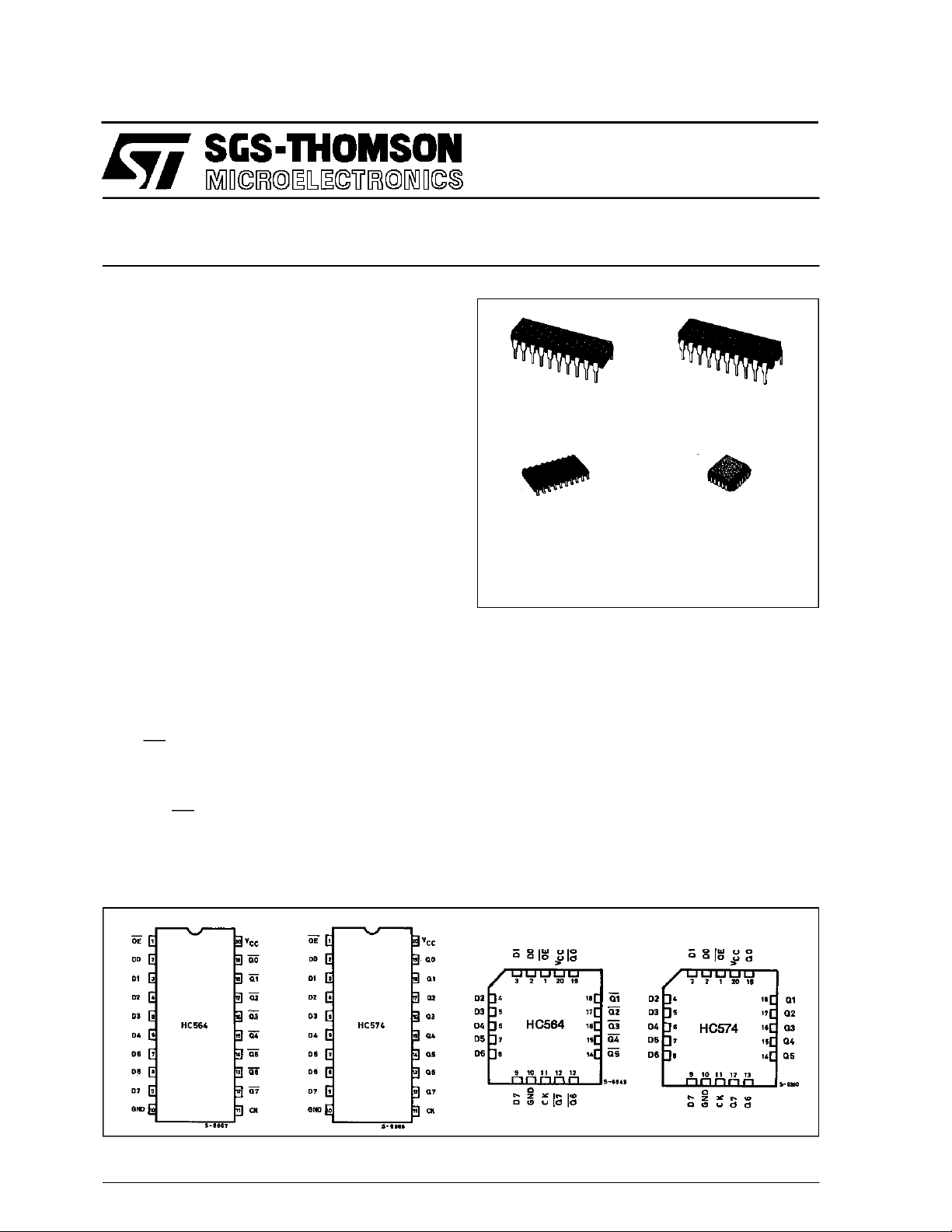
M54/74HC564
M54/ 74 HC5 74
B1R
(PlasticPackage)
M1R
(MicroPackage)
ORDER CODES :
M54HCXXXF1R M74HCXXXM1R
M74HCXXXB1 R M7 4HCXXX C1R
ancestate.The outputcontroldoes notaffecttheinternaloperation offlip-flops.Thatis,theolddatacan
be retained or the new data can be entered even
while the outputs areoff. The application engineer
has a choice of combination of inverting andnon-inverting outputs. The 3-state output configuration
and thewide choice ofoutline make bus-organized
systemssimple.Allinputsareequipped withprotection circuits against static discharge and transient
excessvoltage.
F1R
(CeramicPackage)
C1R
(Chip Carrier)
PIN CONNECTION (top view)
March1993
1/13
M54/M74HC564/574
INPUT AND OUTPUT EQUIVALENT CIRCUIT
PIN DESCRIPTION (HC564)
PIN No SYMBOL NAME AND FUNCTION
1 OE 3 State output Enable
Input (Active LOW)
2, 3, 4, 5,
6, 7, 8, 9,
10
12, 13, 14,
15, 16, 17,
18, 19
11 CLOCK Clock Input (LOW to
10 GND Ground (0V)
20 V
D0 to D7 Data Inputs
Q0 to Q7 3 State outputs
HIGH, edge triggered)
CC
Positive Supply Voltage
IEC LOGIC SYMBOLS
PIN DESCRIPTIO N (HC574)
PIN No SYMBOL NAME AND FUNCTION
1 OE 3 State output Enable
Input (Active LOW)
2, 3, 4, 5,
6, 7, 8, 9,
10
12, 13, 14,
15, 16, 17,
18, 19
11 CLOCK Clock Input (LOW to
10 GND Ground (0V)
20 V
D0 to D7 Data Inputs
Q0 to Q7 3 State outputs
HIGH, edge triggered)
CC
HC574HC564
Positive Supply Voltage
2/13
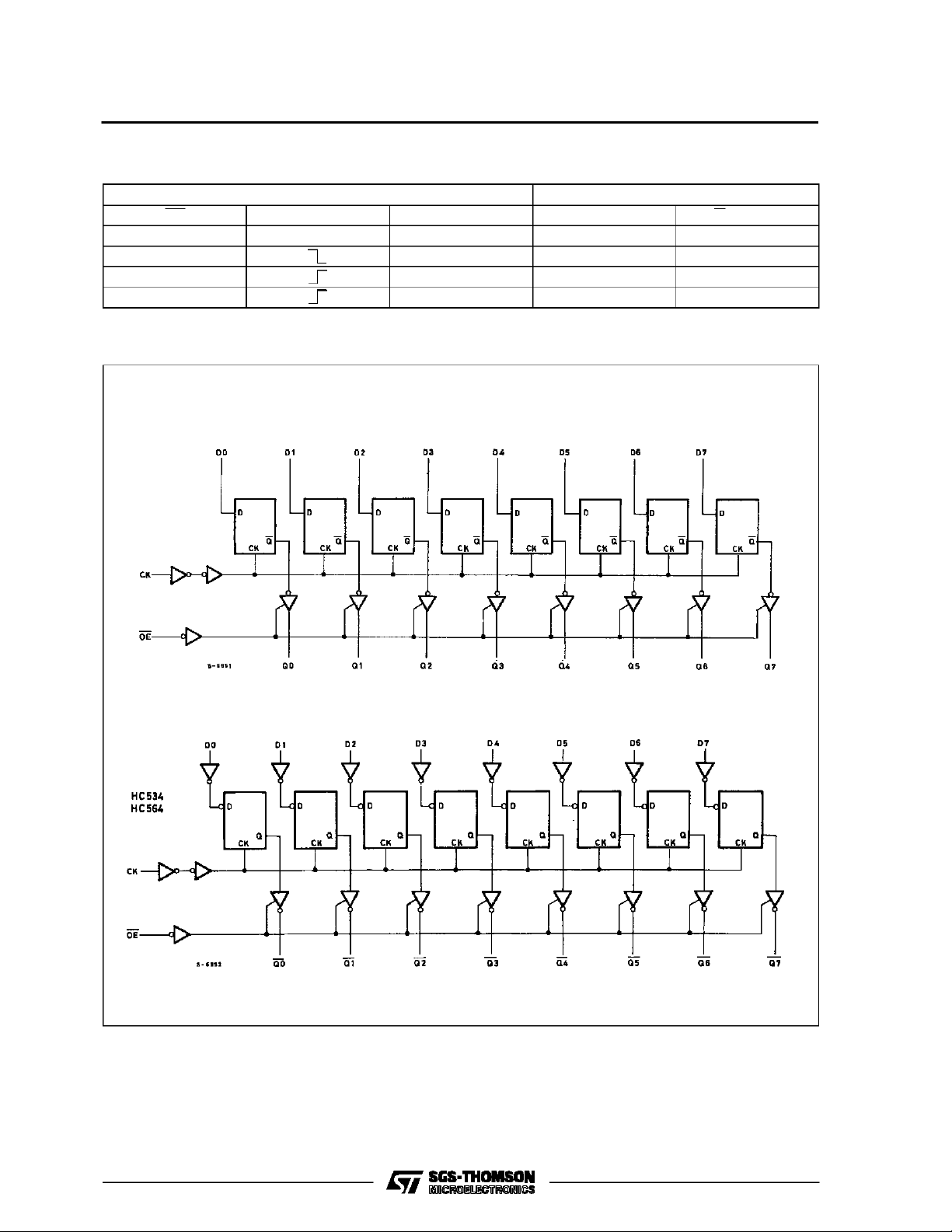
TRUTH TABLE
OE CK D Q (HC574) Q (HC564)
HXXZZ
L X NO CHANGE NO CHANGE
LLLH
LHHL
LOGIC DIAGRAMS
M54/M74HC564/574
INPUTS OUTPUTS
3/13
M54/M74HC564/574
ABSOLU TE M AXIMU M R AT INGS
Symbol Parameter Value Unit
V
CC
V
V
O
I
IK
I
OK
I
O
I
or I
CC
P
D
T
stg
T
AbsoluteMaximumRatingsarethose values beyond whichdamage tothedevicemayoccur. Functionaloperationunder theseconditionisnotimplied.
(*)500 mW:≅ 65oC derate to 300mW by 10mW/oC: 65oCto85oC
RECO MM ENDED OPERAT I N G C ONDITIONS
Symbol Parameter Value Unit
V
CC
V
I
V
O
T
op
t
r,tf
Supply Voltage -0.5 to +7 V
DC Input Voltage -0.5 to VCC+ 0.5 V
I
DC Output Voltage -0.5 to VCC+ 0.5 V
DC Input Diode Current ± 20 mA
DC Output Diode Current ± 20 mA
DC Output Source Sink CurrentPer Output Pin ± 35 mA
DC VCCor Ground Current ± 70 mA
GND
Power Dissipation 500 (*) mW
Storage Temperature -65 to +150
Lead Temperature (10 sec) 300
L
Supply Voltage 2 to 6 V
Input Voltage 0 to V
Output Voltage 0 to V
Operating Temperature: M54HC Series
M74HC Series
CC
CC
-55 to +125
-40 to +85
Input Rise and Fall Time VCC= 2 V 0 to 1000 ns
V
= 4.5 V 0 to 500
CC
V
= 6 V 0 to 400
CC
o
C
o
C
V
V
o
C
o
C
4/13
 Loading...