

Datasheet M74HC4851TTR, M74HC4851RM13TR, M74HC4851M1R Datasheet (SGS Thomson Microelectronics)
SINGLE 8 CHANNEL ANALOG MUX/DEMUX
WITH INJECTION CURRENT PROTECTION
■ LOW POWER DISSIPATION:
I
=2µA(MAX.) at TA=25°C
CC
■ INJECTION CURRENT PROTECTION:
V
<1mV at VCC=5V IIN≤1mA RS≤3.9KΩ
∆OUT
■ "ON"RESISTANCEatT
215Ω TYP. (V
150Ω TYP. (V
160Ω TYP. (V
■ FASTSWITCHING:
t
=8.6ns(TYP.)atTA=25°C, VCC=4.5V
pd
■ WIDE OPERATING SUPPLY VOLTAGE
RANGE: V
■ HIGH NO ISE IMMUNITY:
V
NIH=VNIL
■ PIN AND FUNCTION COMPATIBLE WITH
=3.0V)
CC
=4.5V)
CC
=6V)
CC
=2VTO6V
CC
=28%VCC(MIN.)
SERIES 4051, 4851
■ LATCH-UP PERFORMANCE EXCEEDS
500mA (JESD 17)
■ ESD PERFORMANCE:
HBM > 2000V (JESD22-A114B);
MM > 200V
DESCRIPTION
The M74HC4851 is a s ingle eight-channel analog
MULTIPLEXER/DEMULTIPLEXER fabricated
with silicon gate C
2
MOS technology.
It is pin to pin compatible with the equivalent to
standard HC4051 and MC14051, but feature
injection c urrent effect control. This make this
device expecially suited for usage in automotive
applications where voltages in excess of normal
=25°C:
A
M74HC4851
TSSOPSOP
ORDER CODES
PACKAGE TUBE T & R
SOP M74HC4851M1R M74HC4851RM13TR
TSSOP M74HC4851TTR
logic voltage are c ommon. The injection current
effect control allows signals at disabled input
channels to exceed the supply voltage range or go
down ground without affe cting the signal of the
enabled analog channel. This eliminated the need
for external diode-resistor networks typically esed
to keep the analog channel signals within the
supply voltage range. This a nalog switch is
bidirectional and digitally controlled. It have three
binary con trol inputs A, B, abd C to sel ect 1 of 8 to
be turned on, an d c onnected to the outpu t, and a
INH input to disable all ch annel.
All inputs and outputs are equipped with
protection circui ts against static discharge, giving
them 2KV ESD immunity and transient excess
voltage.
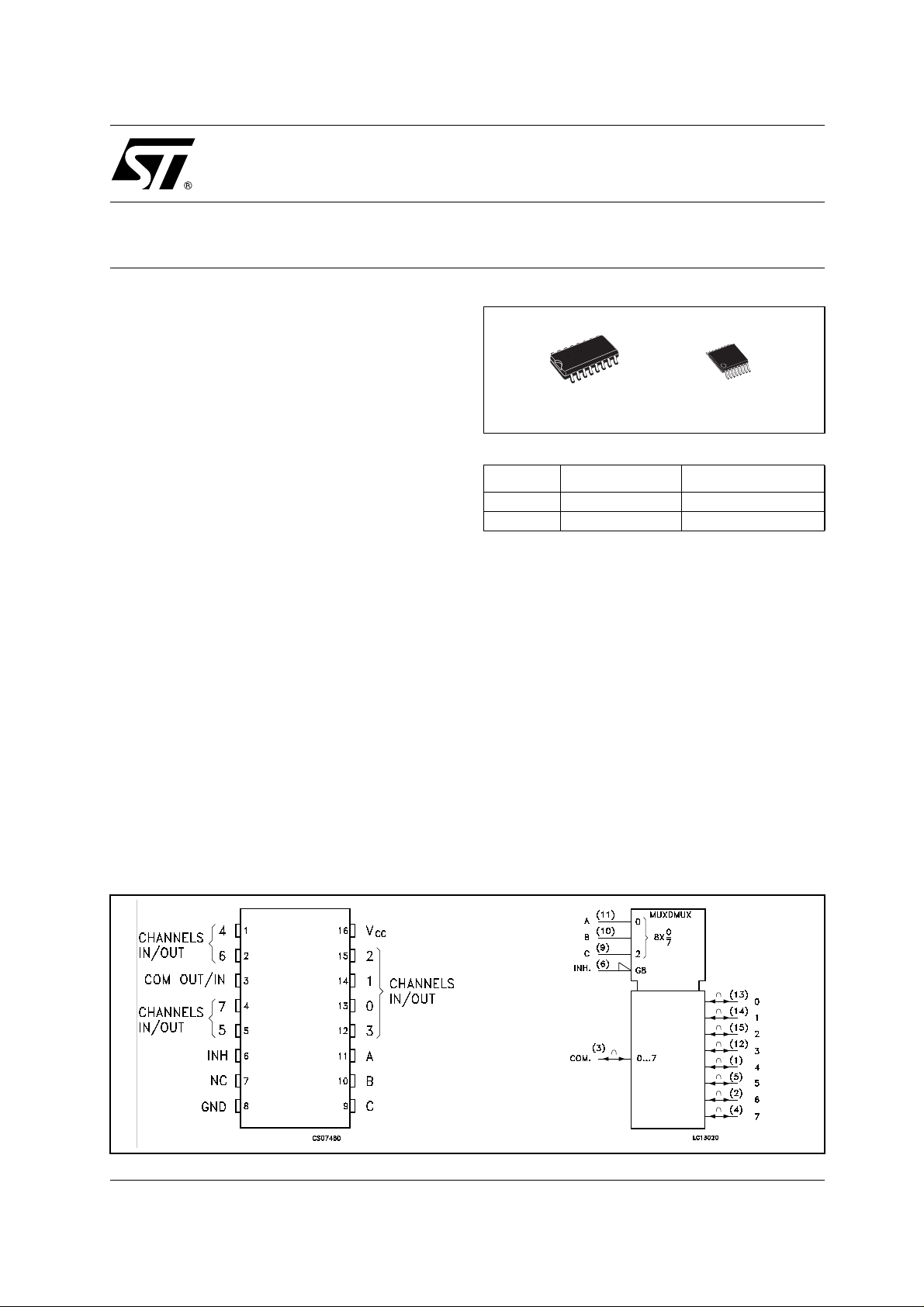
PIN CONNECTION AND IEC LOGIC SYMB OLS
1/11September 2002
M74HC4851
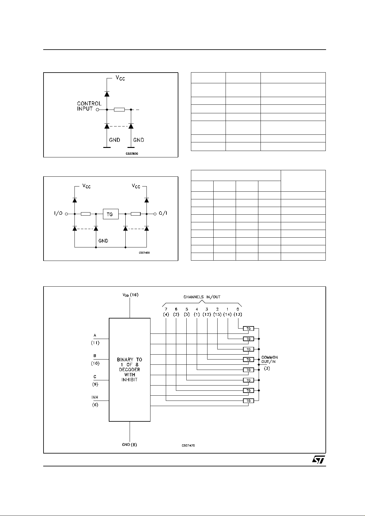
CONTROL INPUT EQUIVALENT CIRCUIT
I/O EQUIVALENT CIRCUIT
PIN DESCRIPTION
PIN No SYMBOL NAME AND FUNCTION
3COM
OUT/IN
6 INH INHIBIT Input
7NC
11, 10, 9 A, B, C Select Inputs
13, 14, 15,
12, 1,5,2,4
8 GND Ground (0V)
16 V
0 to 7 Independent Input/Out-
CC
Common Output/Input
Not Connected
puts
Positive Supply Voltage
TRUTH T ABLE
INPUT STATE
INH C B A
LLLL 0
LLLH 1
LLHL 2
LLHH 3
LHLL 4
LHLH 5
LHHL 6
LHHH 7
H X X X NONE
X: Don’t care
ON CHANNEL
FUNCTIONAL DIAGRAM
2/11
M74HC4851
ABSOLUTE MAXIMUM RATINGS
Symbol Parameter Value Unit
V
V
V
I
CK
I
IOK
I
CC
P
T
T
Absolute Maximum Ratings are those values beyond which damage to the device may occur. Functional operation under these conditions is
not implied
(*) Power difssipation at 65
RECOMMENDED OPERATING CONDITIONS
Symbol Parameter Value Unit
V
V
V
V
T
t
r,tf
1) For voltage drops across switch greater than 1.2V (switch on), excessive Vcc current may drawn; i.e., the current out of the switch may
containbothVCCandswitchinputcomponents.Thereliabilityoft hedevicewillbeunaffectedunlesstheMaximumRatingsareexceeded.
from 30% to 70% VCC of channel Selected or Enable Inputs
2) V
IN
Supply Voltage
CC
Control Input Voltage -0.5 to VCC+ 0.5
IN
Switch I/O Voltage -0.5 to VCC+ 0.5
I/O
Control Input Diode Current
I/O Diode Current
DC VCCor Ground Current
Power Dissipation SOP 500(*) mW
D
-0.5 to +7 V
± 25 mA
± 25 mA
± 50 mA
TSSOP 450(*) mW
Storage Temperature
stg
Lead Temperature (10 sec)
L
-65 to +150 °C
300 °C
°C. Derating from 65°Cto125°C: SO Package -7mW/°C; TSSOPPackage -6.1mW/°C
Supply Voltage
CC
Input Output Voltage 0 to V
I/O
Static or Dynamic Voltage Across Switch (note1) 0 to 1.2
I/O
Control Input Voltage 0 to V
IN
Operating Temperature
op
Input Rise and Fall Time (note2)
(Channel Select or Enable Inputs only)
VCC=2.0V
= 3.0.V
V
CC
=3.3V
V
CC
=4.5V
V
CC
=6.0V
V
CC
2to6 V
CC
CC
-55 to 125 °C
0to1000
0 to 800
0 to 700
0 to 500
0 to 400
V
V
V
V
V
ns
3/11
M74HC4851
DC S PEC IFICATIONS
Symbol Parameter
V
V
R
∆R
I
I
High Level Input
IHC
Voltage
Low Level Input
ILC
Voltage
ON Resistance
ON
Difference of ON
ON
Resistance
between switches
Input/Output
OFF
Leakage Current
(SWITCH OFF)
(Any Channel)
Input/Output
OFF
Leakage Current
(SWITCH OFF)
(Common
Channel)
Switch Input
I
ON
Leakage Current
(SWITCH ON,
OUTPUT OPEN)
I
Control Input
IN
Current
I
Quiescent Supply
CC
Current
Test Condition Value
V
(V)
CC
T
A
Min. Typ. Max. Min. Max. Min. Max.
up to 85°C up to 125°C
= 25°C
2.0 1.5 1.5 1.5
3.0 2.1 2.1 2.1
3.0 2.3 2.3 2.3
4.5 3.15 3.15 3.15
6.0 4.2 4.2 4.2
2.0 0.5 0.5 0.5
3.0 0.9 0.9 0.9
3.3 1.0 1.0 1.0
4.5 1.35 1.35 1.35
6.0 1.8 1.8 1.8
IS=2mA
2.0
3.0
3.3 210 270 305 345
I
≤2mA
S
4.5 160 210 240 270
V
IN=VIHC
V
ILC
VIS=VCCto
GND
or
500 650 670 700
215 280 320 360
6.0 150 195 220 250
=2mA
I
2.0
S
3.0
3.3 2 8 12 16
I
≤2mA
S
4.5 2 8 12 16
V
IN=VIHC
VIS=VCC/2
or
V
ILC
410 15 20
28 12 16
6.0 3 9 13 18
6.0 V
IN=VCC
or GND
±
0.1
± 0.5 ± 1.0
6.0 ± 0.2 ± 2 ± 4
6.0 V
IN=VCC
or GND
±
0.1
± 0.5 ± 1
6.0 VIN=VCCor GND ± 0.1 ± 0.1 ± 1
6.0 VIN=VCCor GND
V
IN(analog)
= GND
22040µA
Unit
V
V
Ω
Ω
µA
µA
µA
µA
4/11

M74HC4851
AC ELECT RICAL CHARACTERISTICS (CL= 50 pF, Input tr=tf=6ns)
Test Condition Value
= 25°C
Symbol Parameter
t
PHL,tPLH
Propagation Delay
Time,Analog Input
to Analog Output
V
CC
(V)
TEST CIRCUIT 1
2.0 19.5 25 29 32
3.0 12 15.5 17.5 19.5
3.3 11 14.5 16.5 18.5
T
A
Min. Typ. Max. Min. Max. Min. Max.
4.5 8.6 11.5 12.5 13.5
6.0 8 10 11 12
t
PHL,tPLH
Propagation Delay
Time
Channel-Select to
Analog Output
2.0 23 30 35 40
3.0 13.5 17.5 20 23
3.3 12.5 16.5 19 22
4.5 10 13 15 17
6.0 9.5 12.5 14.5 16.5
t
PHZtPZH
t
PLZ,tPZL
Enable Disable
Time, Enable or
Channel-Select to
Analog Output
2.0 95 105 115
3.0 90 100 110
3.3 85 95 105
4.5 80 90 100
6.0 78 80 80
Input Capacitance
C
IN
(Digital Pins)
Input Capacitance
C
IN
(Switches Off, Any
Single Analog
3.5 10 10 10
6.7 15 15 15
Pins)
Input Capacitance
C
IN
(Switches Off, Any
Common Analog
22 40 40 40
Pins)
C
(*)CPDis defined as the value of the IC’s internal equivalent capacitance which is calculated from the operating current consumption without
load. (Refer to Test Circuit). Average operating current can be obtained by the following equation. I
Power Dissipation
PD
Capacitance (*)
3.3 24 pF
5.0 28
up to 85°C up to 125°C
CC(opr)=CPDxVCCxfIN+ICC
Unit
ns
ns
ns
pF
pF
pF
/8
INJECTION CURRENT COUPLING SPECIFICATION (TA= -55°C to +125°C)
Test Condition Value
Symbol Parameter
V
Shift of Output
∆OUT
VoltageofEnabled
Analog Channel
1) Typical values are measured at TA=25°C e they are calculate as differance from Vout without Injection Current and Vout with Injection
Current.
= total current injected into any other disabled channels, one at time.
I
IN
V
CC
(V)
3.3
5.0 0.100 1.0
3.3
5.0 0.067 5.0
3.3
5.0 0.110 2.0
3.3
5.0 0.024 20
TEST CIRCUIT 2 Typ.(1) Max.
≤ 1mA, RS ≤ 3.9KΩ
I
IN
I
≤ 10mA, RS ≤ 3.9KΩ
IN
I
≤ 1mA, RS ≤ 20KΩ
IN
I
≤ 10mA, RS ≤ 20KΩ
IN
0.050 1.0 mV
0.345 5.0
0.050 2.0
0.050 20
Unit
5/11

M74HC4851
TEST CIRCUIT 1
TEST SWITCH
t
PLH,tPHL
t
PZL,tPLZ
t
PZH,tPHZ
CL=50pF or equivalent (includes jig and probe capacitance)
RL=R1=10KΩ or equivalent
RT=Z
of pulse generator (typically 50Ω)
OUT
Open
V
CC
GND
TEST CIRCUIT 2
6/11

WAVEFORM: P RO PAGATION DELAY (f=1MHz; 50% duty cycle)
M74HC4851
WAVEFORM: P RO PAGATION DELAY (f=1MHz; 50% duty cycle)
7/11

M74HC4851
WAVEFORM: P RO PAGATION DELAY (f=1MHz; 50% duty cycle)
CHANNEL RESISTANCE (R
ON)
ICC(Opr.)
8/11

SO-16 MECHANICAL DATA
M74HC4851
DIM.
A 1.75 0.068
a1 0.1 0.2 0.003 0.007
a2 1.65 0.064
b 0.35 0.46 0.013 0.018
b1 0.19 0.25 0.007 0.010
C 0.5 0.019
c1 45˚ (typ.)
D 9.8 10 0. 385 0. 393
E 5.8 6. 2 0.228 0. 244
e 1.27 0.050
e3 8.89 0.350
F 3.8 4.0 0.149 0.157
G 4.6 5.3 0.181 0.208
L 0.5 1.27 0.019 0. 050
M 0.62 0.024
S ˚ (max.)
MIN. TYP MAX. MIN. TYP. MAX.
mm. inch
8
PO13H
9/11

M74HC4851
TSSOP16 MECHANICAL DATA
mm. inch
DIM.
MIN. TYP MAX. MIN. TYP. MAX.
A 1.2 0.047
A1 0.05 0.15 0.002 0.004 0.006
A2 0.8 1 1.05 0.031 0.039 0.041
b 0.19 0.30 0.007 0.012
c 0.09 0.20 0.004 0.0089
D 4.9 5 5.1 0.193 0.197 0.201
E 6.2 6.4 6.6 0.244 0.252 0.260
E1 4.3 4.4 4.48 0.169 0.173 0.176
e 0.65 BSC 0.0256 BSC
K0˚ 8˚0˚ 8˚
L 0.45 0.60 0.75 0.018 0.024 0.030
A2
A
A1
b
e
c
K
L
E
D
E1
PIN 1 IDENTIFICATION
10/11
1
0080338D

M74HC4851
Information furnished is believed to be accurate and reliable. However, STMicroelectronics assum es no r esponsibility for t he
consequences of use of such informatio n nor for any infringement of paten ts or o ther rig hts of t hird part ies which ma y result from
its use. No license is granted by implication or otherwise under any patent or patent rights of STMicroelectronics. Specifications
mentioned in this publicatio n are subject to change without notice. This publication supersedes and replaces all information
previousl y suppl ied. STM icroel ectronics produc ts are not auth orized for use as c ritica l compone nts in l ife s upport dev ices or
systems without express written approval of STMicroelectronics.
Australia - Brazil - Canada - China - Finland - France - Germany - Hong Kong - India - Israel - Italy - Japan - Malaysia - Malta - Morocco
© The ST logo is a registered trademark of STMicroelectronics
© 2002 STMicroelectronics - Printed in Italy - All Rights Reserved
STMicroelectronics GROUP OF COMPANIES
Singapore - Spain - Sweden - Switzerland - United Kingdom - United States.
© http://www.st.com
11/11
 Loading...