

SGS Thomson Microelectronics M74HC4520, M74HC4518 Datasheet
HC4518 DUAL DECADE COUNTER
HC4520 DUAL 4 BIT BINARY COUNTER
.HIGH SPEED
f
= 55 MHz (TYP.) at VCC=5V
MAX
.LOWPOWER DISSIPATION
ICC=4µA(MAX.) AT TA=25°C
.HIGH NOISE IMMUNITY
V
NIH=VNIL
=28%VCC(MIN.)
.OUTPUT DRIVE CAPABILITY
10 LSTTL LOADS
.SYMMETRICAL OUTPUT IMPEDANCE
|IOH|=IOL=4 mA (MIN.)
.BALANCEDPROPAGATION DELAYS
t
PLH=tPHL
.WIDE OPERATING VOLTAGE RANGE
VCC(OPR)= 2 V TO6 V
.PIN AND FUNCTION COMPATIBLE WITH
4520B/4518B
M54/M74HC4518
M54/M74HC4520
B1R
(PlasticPackage)
M1R
(MicroPackage)
ORDER CODES :
M54HC XXXXF1R M74HCXXXXM1R
M74HC XXXXB1R M74HCXXXXC 1R
F1R
(CeramicPackage)
C1R
(Chip Carrier)
DESCRIPTION
The M54/74HC4518/4520 are high speed CMOS
DUAL 4 BIT BINARYCOUNTERSfabricated in silicon gate C2MOS technology. They have the same
high speed performance of LSTTL combined with
true CMOS low power consumption.
They consists of two identical internally synchronous 4-stagecounters. The counter stages are
D-type flip-flops having interchangeable Clock and
ENABLE inputsfor incrementing oneither the positive-goingor negative-going transition.
Forsingle-unit operation theENABLE inputismaintained ”high” and the counter advances on each
positive-going transition of the CLOCK. The
counters are cleared by high levels on their clear
lines. The counter can be cascaded in the ripple
mode by connecting Q4 to the enable input of the
subsequentcounter whiletheclockinput ofthe latter
is heldpermanently low.
All inputs are equipped with protection circuits
against static discharge and transient excess voltage.
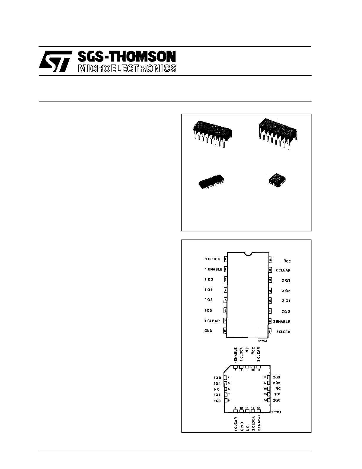
PIN CONNECTIONS(top view)
NC =
No Internal
Connection
March1993
1/13
M54/M74HC4518/4520
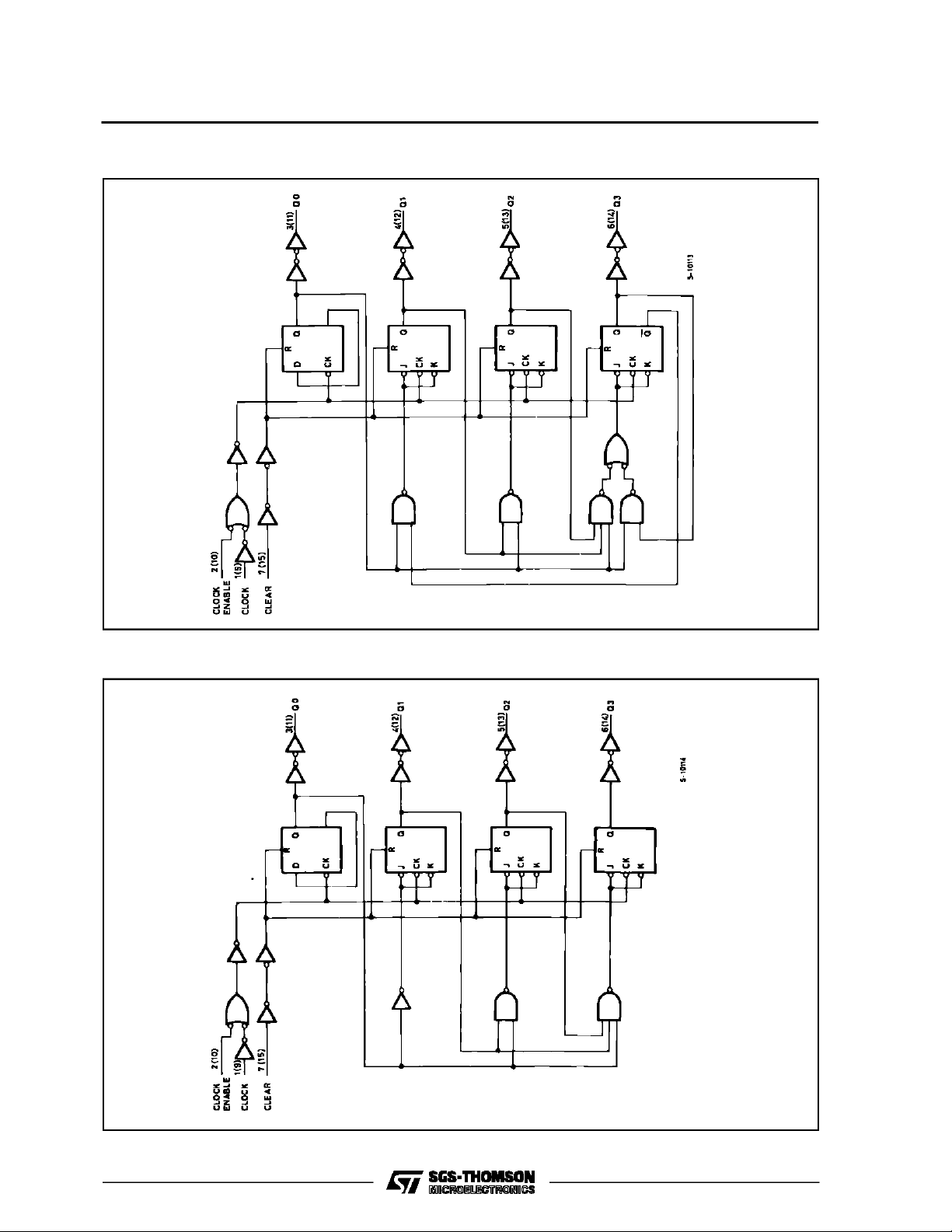
LOGIC DIAGRAM (1/2 HC4518)
LOGIC DIAGRAM (1/2 HC4520)
2/13
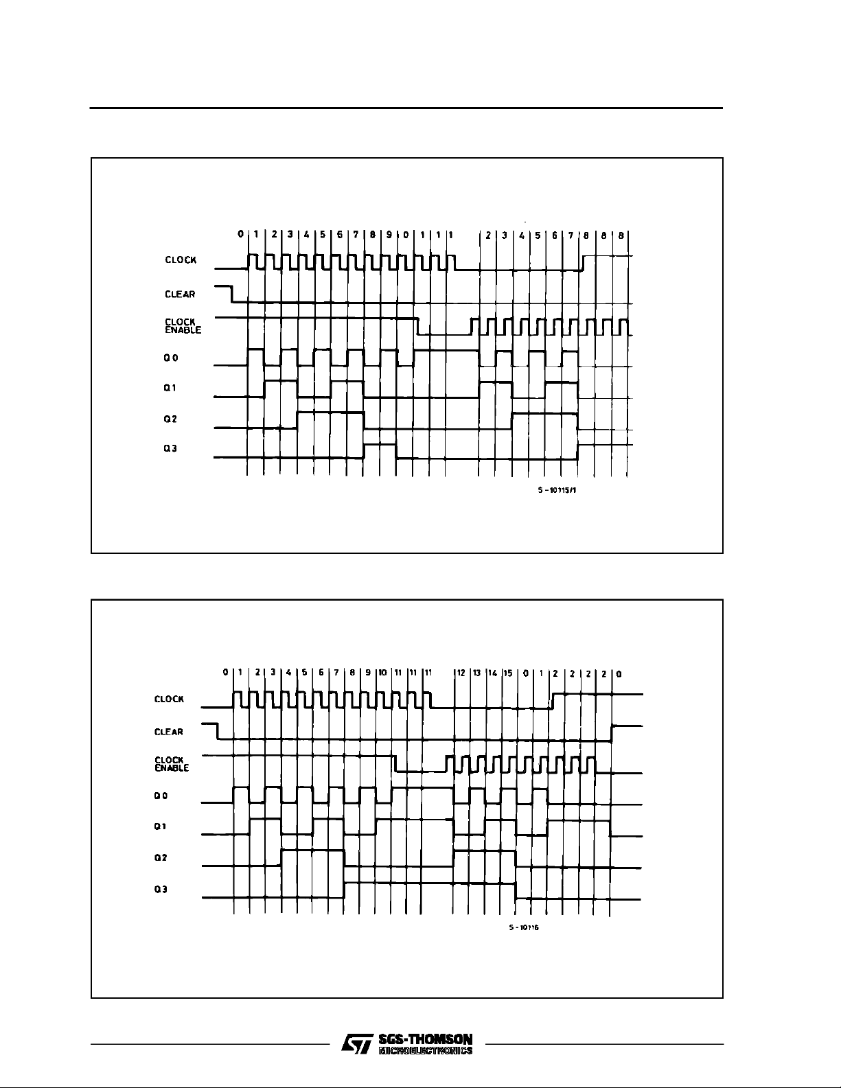
TIMING CHART (HC4518)
M54/M74HC4518/4520
TIMING CHART (HC4520)
3/13
M54/M74HC4518/4520
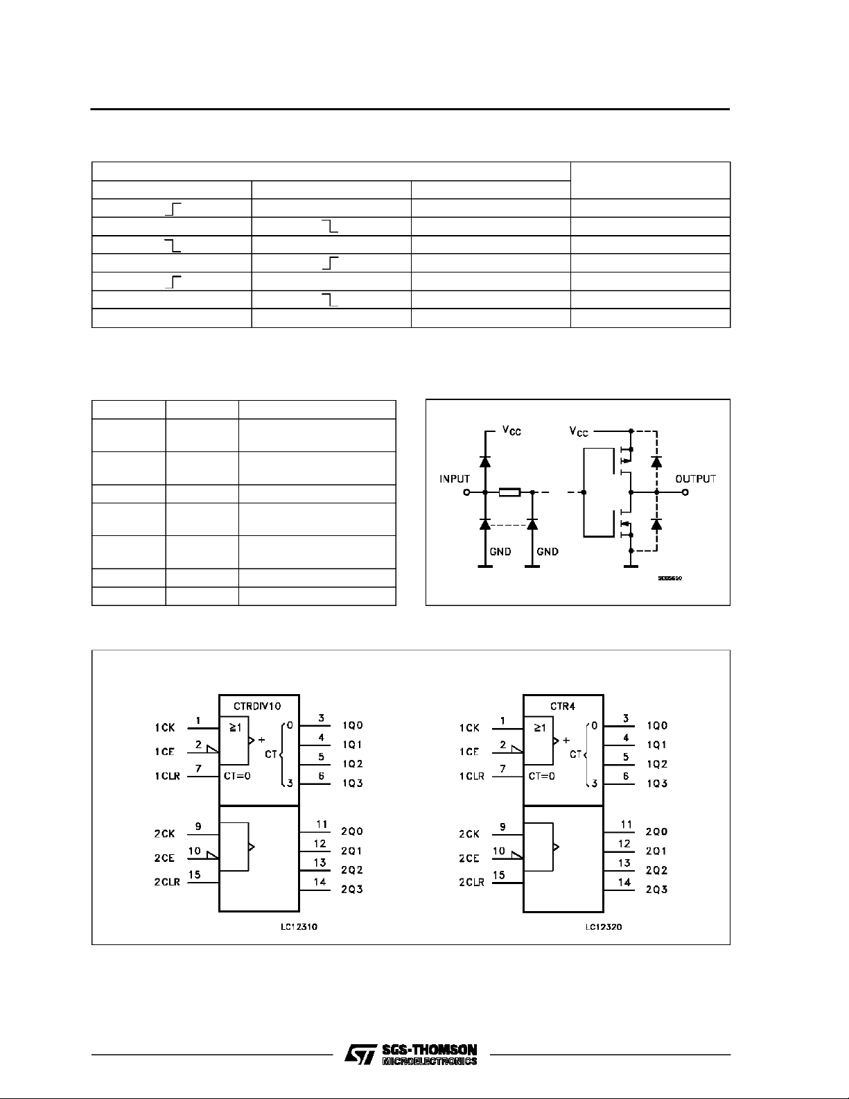
TRUTH TABLE
INPUTS
CLOCK ENABLE CLEAR
H L INCREMENT COUNTER
L L INCREMENT COUNTER
X L NO CHANGE
X L NO CHANGE
L L NO CHANGE
H L NO CHANGE
X X H Q0 THRU Q3 = L
X:Don’tCare Z: HighImpedance
PIN No SYMBOL NAME AND FUNCTION
1, 9 1CLOCK,
2CLOCK
2, 10 1ENABLE,
2ENABLE
3, 4, 5, 6 1Q0 to 1Q3 Data Outputs
7, 15 1CLEAR,
2CLEAR
11, 12, 13,142Q0 to 2Q3 Data Outputs
Clock Inputs (LOW to
HIGH, Edge-triggered)
Clock Enable Inputs
Asynchronous Reset
Inputs (Active LOW)
FUNCTION
INPUT AND OUTPUT EQUIVALENT CIRCUITPIN DESCRIPTION
8 GND Ground (0V)
16 V
CC
IEC LOGIC SYMBOLS
HC4518 HC452 0
Positive Supply Voltage
4/13
 Loading...