

HC45 14: 4 TO 16 LINE DECODER/LATCH
HC4515: 4 TO 16 LINEDECODER LATCH(INV.)
.HIGH SPEED
tPD= 18 ns(TYP.) AT VCC=5V
.LOWPOWERDISSIPATION
ICC=4µA(MAX.) AT TA=25°C
.HIGH NOISEIMMUNITY
V
NIH=VNIL
=28%VCC(MIN.)
.OUTPUT DRIVE CAPABILITY
10 LSTTL LOADS
.SYMMETRICALOUTPUT IMPEDANCE
|IOH|=IOL=4 mA(MIN.)
.BALANCEDPROPAGATION DELAYS
t
PLH=tPHL
.WIDE OPERATINGVOLTAGE RANGE
VCC(OPR)= 2 V TO6 V
.PIN AND FUNCTION COMPATIBLE WITH
4514B/4515B
M74HC4514
M74HC4515
B1R
(PlasticPackage)
ORDER CODES :
M74HCXXXXM1R M74HCXXXXB1 R
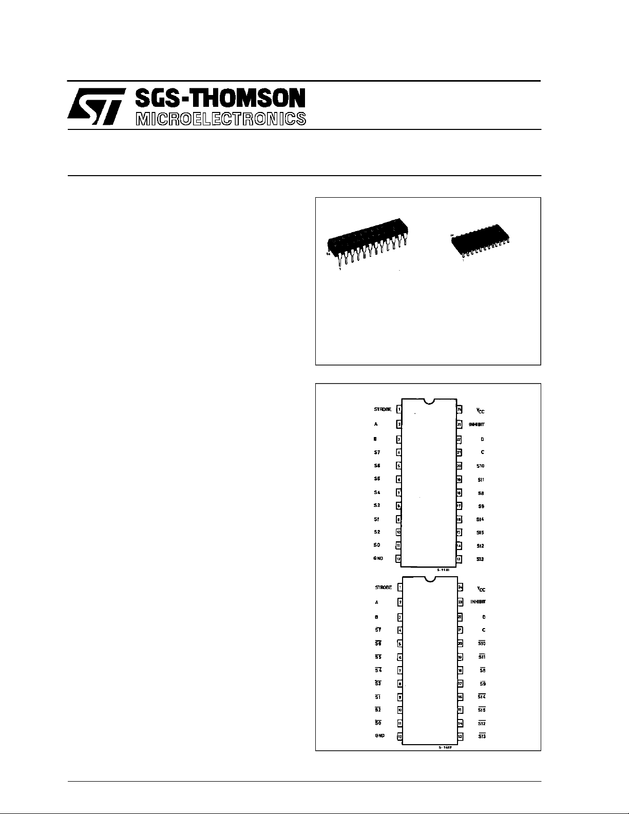
PIN CONNECTIONS (top view)
HC4514
M1R
(MicroPackage)
DESCRIPTION
The 74HC4514 andthe 74HC4515 are high speed
CMOS 4-LINE TO 16-LINE DECODERS WITH
LATCHED INPUTS fabricated in silicon gate
C2MOS technology. They have the same high
speed performance of LSTTL combined with true
CMOS low powerconsumption.
A binary code stored in the four input latches (A to
D) provides a high level (HC4514) or a low level
(HC4515) at the selectedone ofsixteenoutputs excluding the other fifteen outputs, when the inhibit
input(INHIBIT) is held low. When theinhibit input is
heldhigh, all outputsare keptlowlevel (HC4514) or
highlevel(HC4515), whilethelatchfunctionisavailable.The data applied to the datainputs are transfered to the Q outputs of latches when the strobe
input is held high. When the strobe input is taken
low,the information dataappliedto thedata input at
a time is retained at theoutput of thelatches. All inputs are equipped with protection circuits against
staticdischarge and transient excessvoltage.
October 1993
HC4515
1/10
M74HC4514/4515
TRUTH TABLE
INPUTS
INHIBIT ABCD
STROBE
L L L L L STROBE = ’H’
L H L L L S1 (S1)
L L H L L S2 (S2)
L H H L L S3 (S3)
L L L H L S4 (S4)
L H L H L S5 (S5)
L L H H L S6 (S6)
Refer to truth table
STROBE = ’L’
Data at the negative going
transition of strobe shall be
provided on the each output
while strobe is held low.
SELECT OUTPUT
HC4514 - ’H’
(HC4515 - ’L’)
S0 (S0)
L H H H L S7 (S7)
t
L L L L H S8 (S8)
n-1
t
n
L H L L H S9 (S9)
L L H L H S10 (S10)
L H H L H S11 (S11)
L L L H H S12 (S12)
L H L H H S13 (S13)
STROBE
L L H H H S14 (S14)
L HHHH S15(S15)
H XXXX HC4514 - ALL OUTPUTS ’L’
(HC4515 - ALL OUTPUTS ’H’)
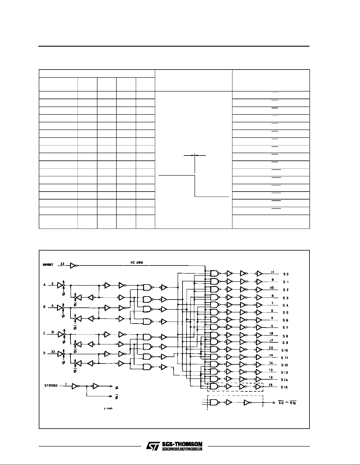
LOGIC DIAGRAM (HC4514)
FORHC4515 DEVICE LOGIC DIAGRAMSHOWN AT THEBOTTOM SHALL TAKE THE PLACEOF OUTPUTCIRCUITS.
2/10
M7 4HC4 514/4515
PIN DESC RIPTION (H C4514)
PIN No SYMBOL NAME AND FUNCTION
1 STROBE Strobe Input
2, 3, 21, 22 A to D Address Inputs
11, 9, 10, 8,
7, 6, 5, 4,
18, 17, 20,
19, 14, 13,
16, 15
23 INHIBIT Enable Input
12 GND Ground (0V)
24 V
S0 to S15 Multiplexer Outputs
(Active HIGH)
CC
Positive Supply Voltage
IEC LOGIC SYMBOLS
PIN DESCRIPTION (HC4515)
PIN No SYMBOL NAME AND FUNCTION
1 STROBE Strobe Input
2, 3, 21, 22 A to D Address Inputs
11, 9, 10, 8,
7, 6, 5, 4,
18, 17, 20,
19, 14, 13,
16, 15
23 INHIBIT Enable Input
12 GND Ground (0V)
24 V
HC451 4
S0 to S15 Multiplexer Outputs
CC
(Active LOW)
Positive Supply Voltage
HC451 5
3/10

M74HC4514/4515
INPUT AND OUTPUT EQUIVALENT CIRCUIT
ABSOLU TE MAXI MU M RATING S
Symbol Parameter Value Unit
V
CC
V
V
O
I
IK
I
OK
I
O
or I
I
CC
P
D
T
stg
T
L
AbsoluteMaximumRatingsarethose values beyondwhichdamage tothedevicemayoccur. Functionaloperationunder these conditionisnotimplied.
(*)500 mW: ≅ 65oC derateto300mWby 10mW/oC: 65oCto85oC
Supply Voltage -0.5 to +7 V
DC Input Voltage -0.5 to VCC+ 0.5 V
I
DC Output Voltage -0.5 to VCC+ 0.5 V
DC Input Diode Current ± 20 mA
DC Output Diode Current ± 20 mA
DC Output Source Sink Current Per Output Pin ± 25 mA
DC VCCor Ground Current ± 50 mA
GND
Power Dissipation 500 (*) mW
Storage Temperature -65 to +150
Lead Temperature (10sec) 300
o
C
o
C
RECO MM ENDED OPERATIN G CO NDI TIONS
Symbol Parameter Value Unit
Supply Voltage 2 to 6 V
CC
Input Voltage 0 to V
I
Output Voltage 0 to V
O
Operating Temperature -40 to +85
op
CC
CC
Input Rise and Fall Time VCC= 2 V 0 to 1000 ns
V
= 4.5 V 0 to 500
CC
= 6 V 0 to 400
V
CC
4/10
V
T
t
V
V
r,tf
V
V
o
C

DC SPECIFICATIONS
Symbol Parameter
V
V
V
V
I
I
High Level Input Voltage 2.0 1.5 1.5
IH
Low Level Input
IL
Voltage
High Level Output Voltage 2.0
OH
Low Level Output Voltage 2.0
OL
Input Leakage Current 6.0 VI=VCCor GND ±0.1 ±1 µA
I
I
3 State Output Off State Current 6.0 VI=VIHor V
OZ
Quiescent Supply Current 6.0 VI=VCCor GND 4 40 µA
CC
M7 4HC4 514/4515
Test Conditions Value
V
CC
(V)
4.5 3.15 3.15
6.0 4.2 4.2
2.0 0.5 0.5
4.5 1.35 1.35
6.0 1.8 1.8
=
V
I
V
IH
or
V
IL
V
I
V
IH
or
V
IL
IO=-20 µA
=-4.0 mA 4.18 4.31 4.13
O
=-5.2 mA 5.68 5.8 5.63
O
=
IO=20µA
= 4.0 mA 0.17 0.26 0.33
O
= 5.2 mA 0.18 0.26 0.33
O
IL
4.5 4.4 4.5 4.4
6.0 5.9 6.0 5.9
4.5 I
6.0 I
4.5 0.0 0.1 0.1
6.0 0.0 0.1 0.1
4.5 I
6.0 I
VO=VCCor GND
TA=25oC -40 to 85oC
Min. Typ. Max. Min. Max.
1.9 2.0 1.9
0.0 0.1 0.1
±0.5 ±5.0 µA
Unit
V
V
V
V
5/10
M74HC4514/4515
AC ELECTRICAL CHARACTERI STI CS (CL=50pF,Inputtr=tf=6ns)
Test Conditions Value
Symbol Parameter
t
t
TLH
THL
Output Transition Time 2.0 30 75 95
V
CC
(V)
4.5 8 15 19
TA=25oC -40 to 85oC
Min. Typ. Max. Min. Max.
6.0 7 13 16
t
t
PLH
PHL
Propagation Delay Time
(DATA - Sn, Sn)
2.0 65 175 220
4.5 22 35 44
6.0 19 30 37
t
t
PHL
PLH
Propagation Delay Time
(STROBE- Sn, Sn)
2.0 75 175 220
4.5 24 35 44
6.0 20 30 37
t
t
PHL
PLH
Propagation Delay Time
(INH IBIT- Sn,Sn)
2.0 60 175 220
4.5 20 35 44
6.0 17 30 37
t
W(L)
Minimum Pulse Width
(STROBE)
2.0 14 75 95
4.5 6 15 19
6.0 6 13 16
Minimum Set-up Time
t
s
(DATA)
2.0 10 50 65
4.5 2 10 13
6.0 2 9 11
t
Minimum Hold Time
h
(DATA)
2.0 5 5
4.5 5 5
6.0 5 5
C
C
PD
(*) CPDisdefined as the value ofthe IC’sinternal equivalent capacitance whichis calculated fromthe operatingcurrentconsumption without load.
(Referto Test Circuit). Average operting current canbe obtained bythefollowingequation. ICC(opr) = CPD•VCC•fIN+I
Input Capacitance 5 10 10 pF
IN
(*) Power Dissipation Capacitance 61 pF
CC
Unit
ns
ns
ns
ns
ns
ns
ns
6/10

SWITCHING CHARACTERISTICS TEST WAVEFORM
M7 4HC4 514/4515
TEST CIRCUIT ICC(Opr.)
INPUTWAVEFORMIS THESAMEASTHAT IN CASE OF SWITCHINGCHARACTERISTICSTEST.
7/10

M74HC4514/4515
Plastic DIP24 (0.25) MECHANICAL DATA
DIM.
MIN. TYP. MAX. MIN. TYP. MAX.
a1 0.63 0.025
b 0.45 0.018
b1 0.23 0.31 0.009 0.012
b2 1.27 0.050
D 32.2 1.268
E 15.2 16.68 0.598 0.657
e 2.54 0.100
e3 27.94 1.100
F 14.1 0.555
I 4.445 0.175
L 3.3 0.130
mm inch
8/10
P043A
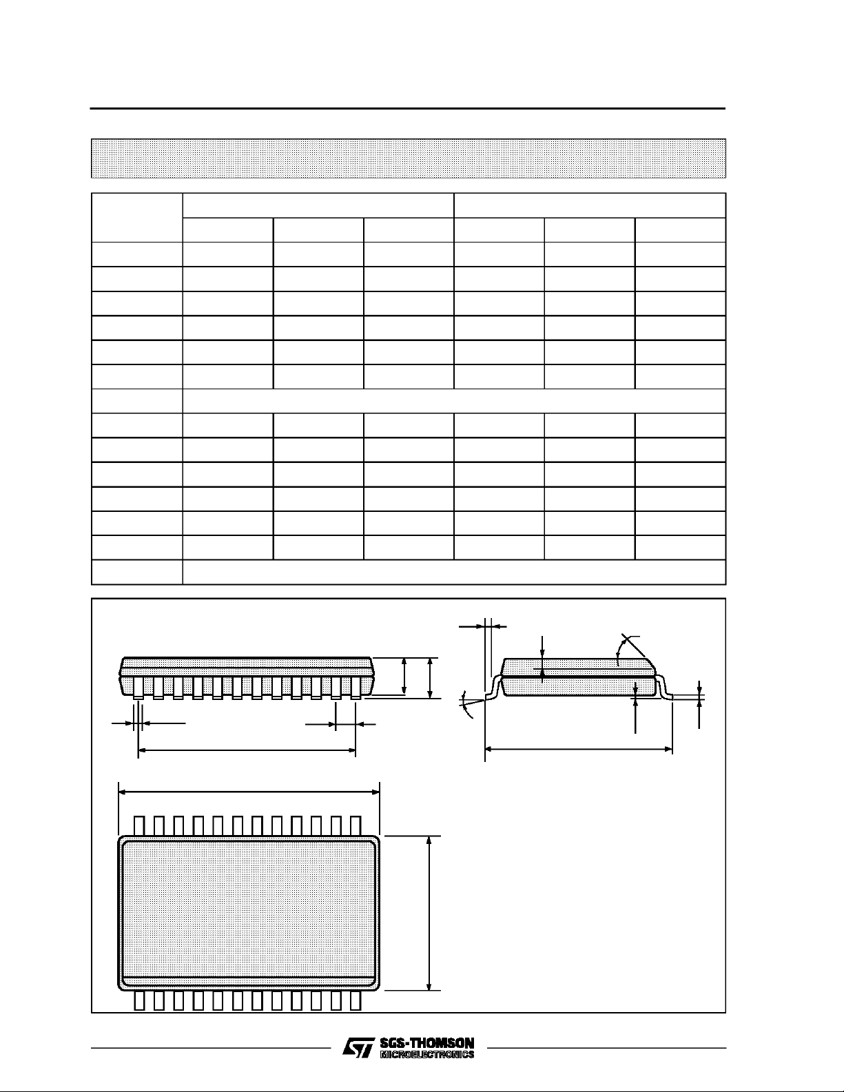
SO24 MECHANICAL DATA
M7 4HC4 514/4515
DIM.
MIN. TYP. MAX. MIN. TYP. MAX.
A 2.65 0.104
a1 0.10 0.20 0.004 0.007
a2 2.45 0.096
b 0.35 0.49 0.013 0.019
b1 0.23 0.32 0.009 0.012
C 0.50 0.020
c1 45° (typ.)
D 15.20 15.60 0.598 0.614
E 10.00 10.65 0.393 0.420
e 1.27 0.05
e3 13.97 0.55
F 7.40 7.60 0.291 0.299
L 0.50 1.27 0.19 0.050
S8°(max.)
mm inch
L
A
a2
b
e3
D
24 13
112
e
F
s
a1
c1
b1
C
E
9/10

M74HC4514/4515
Information furnishedis believed to be accurate and reliable. However, SGS-THOMSON Microelectronicsassumes no responsability for the
consequences of useof suchinformation nor forany infringement of patents or other rights of third parties which may results from its use. No
license is granted byimplication or otherwiseunder any patentor patentrights ofSGS-THOMSON Microelectronics.Specificationsmentioned
in this publication are subjectto changewithout notice. This publication supersedes andreplaces all information previously supplied.
SGS-THOMSON Microelectronicsproducts are not authorized foruse ascritical componentsinlife supportdevices orsystemswithoutexpress
written approval of SGS-THOMSON Microelectonics.
1994SGS-THOMSON Microelectronics- All Rights Reserved
Australia -Brazil - France - Germany - Hong Kong - Italy - Japan - Korea - Malaysia - Malta -Morocco - The Netherlands-
Singapore -Spain - Sweden- Switzerland - Taiwan - Thailand- UnitedKingdom - U.S.A
SGS-THOMSON Microelectronics GROUP OFCOMPANIES
10/10
 Loading...