

SGS Thomson Microelectronics M74HC4515, M74HC4514 Datasheet
HC45 14: 4 TO 16 LINE DECODER/LATCH
HC4515: 4 TO 16 LINEDECODER LATCH(INV.)
.HIGH SPEED
tPD= 18 ns(TYP.) AT VCC=5V
.LOWPOWERDISSIPATION
ICC=4µA(MAX.) AT TA=25°C
.HIGH NOISEIMMUNITY
V
NIH=VNIL
=28%VCC(MIN.)
.OUTPUT DRIVE CAPABILITY
10 LSTTL LOADS
.SYMMETRICALOUTPUT IMPEDANCE
|IOH|=IOL=4 mA(MIN.)
.BALANCEDPROPAGATION DELAYS
t
PLH=tPHL
.WIDE OPERATINGVOLTAGE RANGE
VCC(OPR)= 2 V TO6 V
.PIN AND FUNCTION COMPATIBLE WITH
4514B/4515B
M74HC4514
M74HC4515
B1R
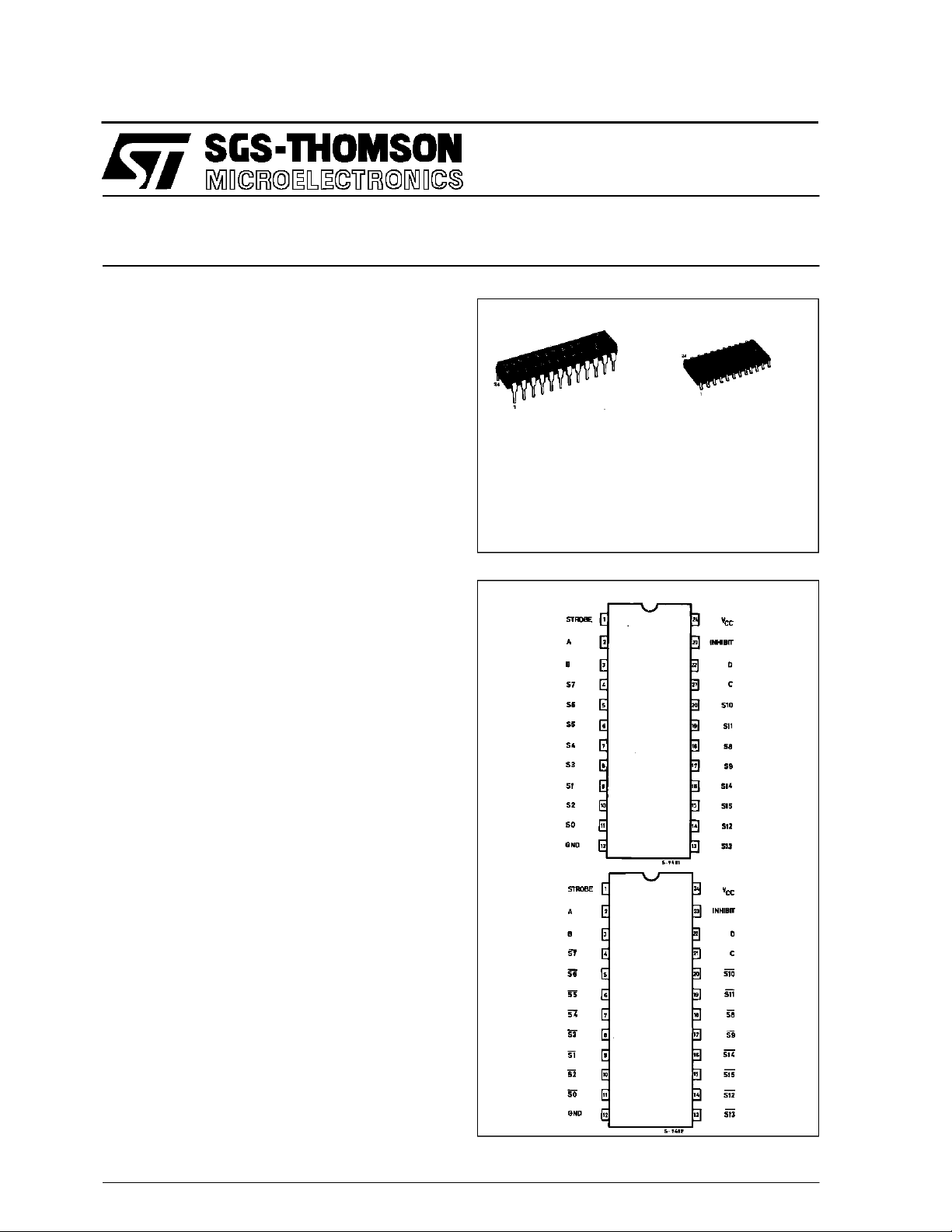
(PlasticPackage)
ORDER CODES :
M74HCXXXXM1R M74HCXXXXB1 R
PIN CONNECTIONS (top view)
HC4514
M1R
(MicroPackage)
DESCRIPTION
The 74HC4514 andthe 74HC4515 are high speed
CMOS 4-LINE TO 16-LINE DECODERS WITH
LATCHED INPUTS fabricated in silicon gate
C2MOS technology. They have the same high
speed performance of LSTTL combined with true
CMOS low powerconsumption.
A binary code stored in the four input latches (A to
D) provides a high level (HC4514) or a low level
(HC4515) at the selectedone ofsixteenoutputs excluding the other fifteen outputs, when the inhibit
input(INHIBIT) is held low. When theinhibit input is
heldhigh, all outputsare keptlowlevel (HC4514) or
highlevel(HC4515), whilethelatchfunctionisavailable.The data applied to the datainputs are transfered to the Q outputs of latches when the strobe
input is held high. When the strobe input is taken
low,the information dataappliedto thedata input at
a time is retained at theoutput of thelatches. All inputs are equipped with protection circuits against
staticdischarge and transient excessvoltage.
October 1993
HC4515
1/10
M74HC4514/4515
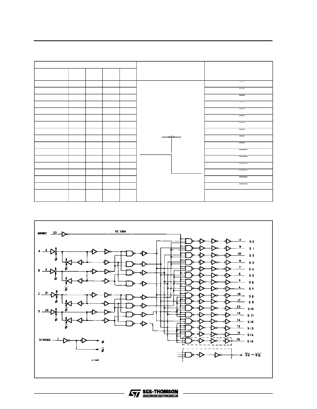
TRUTH TABLE
INPUTS
INHIBIT ABCD
STROBE
L L L L L STROBE = ’H’
L H L L L S1 (S1)
L L H L L S2 (S2)
L H H L L S3 (S3)
L L L H L S4 (S4)
L H L H L S5 (S5)
L L H H L S6 (S6)
Refer to truth table
STROBE = ’L’
Data at the negative going
transition of strobe shall be
provided on the each output
while strobe is held low.
SELECT OUTPUT
HC4514 - ’H’
(HC4515 - ’L’)
S0 (S0)
L H H H L S7 (S7)
t
L L L L H S8 (S8)
n-1
t
n
L H L L H S9 (S9)
L L H L H S10 (S10)
L H H L H S11 (S11)
L L L H H S12 (S12)
L H L H H S13 (S13)
STROBE
L L H H H S14 (S14)
L HHHH S15(S15)
H XXXX HC4514 - ALL OUTPUTS ’L’
(HC4515 - ALL OUTPUTS ’H’)
LOGIC DIAGRAM (HC4514)
FORHC4515 DEVICE LOGIC DIAGRAMSHOWN AT THEBOTTOM SHALL TAKE THE PLACEOF OUTPUTCIRCUITS.
2/10
M7 4HC4 514/4515
PIN DESC RIPTION (H C4514)
PIN No SYMBOL NAME AND FUNCTION
1 STROBE Strobe Input
2, 3, 21, 22 A to D Address Inputs
11, 9, 10, 8,
7, 6, 5, 4,
18, 17, 20,
19, 14, 13,
16, 15
23 INHIBIT Enable Input
12 GND Ground (0V)
24 V
S0 to S15 Multiplexer Outputs
(Active HIGH)
CC
Positive Supply Voltage
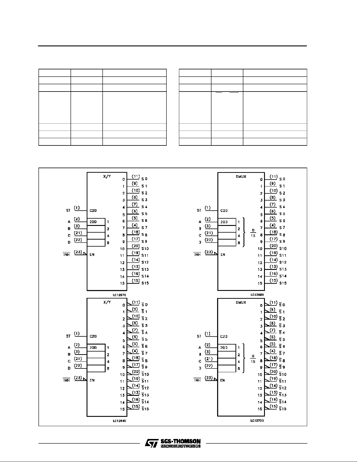
IEC LOGIC SYMBOLS
PIN DESCRIPTION (HC4515)
PIN No SYMBOL NAME AND FUNCTION
1 STROBE Strobe Input
2, 3, 21, 22 A to D Address Inputs
11, 9, 10, 8,
7, 6, 5, 4,
18, 17, 20,
19, 14, 13,
16, 15
23 INHIBIT Enable Input
12 GND Ground (0V)
24 V
HC451 4
S0 to S15 Multiplexer Outputs
CC
(Active LOW)
Positive Supply Voltage
HC451 5
3/10
 Loading...