

BCD TO 7 SEGMENT LATCH/DECODER DRIVER
.HIGH SPEED
tPD= 28 ns(TYP.) AT VCC=5V
.LOWPOWER DISSIPATION
ICC=4µA(MAX.) AT TA=25°C
.HIGH NOISE IMMUNITY
V
NIH=VNIL
=28%VCC(MIN.)
.OUTPUT DRIVE CAPABILITY
10 LSTTLLOADS
.HIGH SOURGECURRENT
|IOH| =20 mA(MIN.)
.BALANCEDPROPAGATION DELAYS
t
PLH=tPHL
.WIDE OPERATINGVOLTAGE RANGE
VCC(OPR)= 2 V TO6 V
.PIN ANDFUNCTION COMPATIBLE
WITH 4511B
M54HC4511
M74HC4511
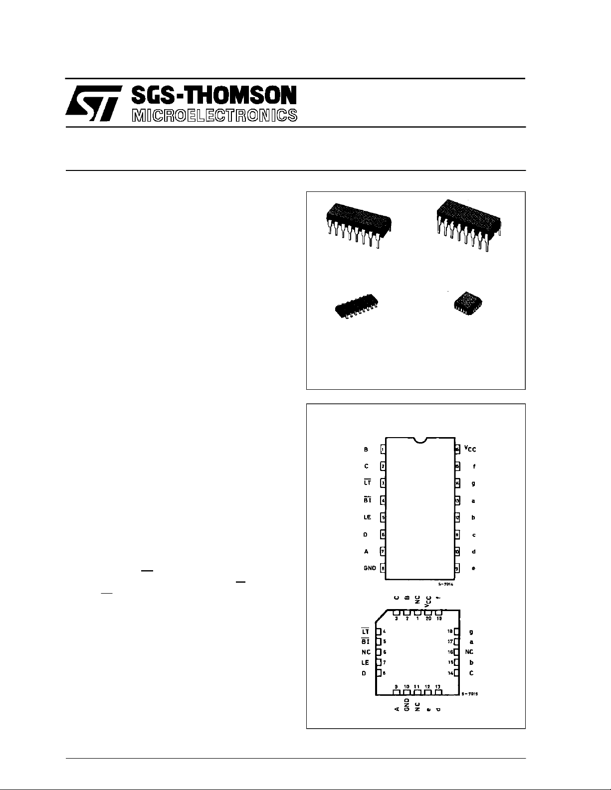
B1R
(PlasticPackage)
M1R
(MicroPackage)
ORDER CODES :
M54HC 4011F1R M74H C4011M1R
M74HC 4011B1R M74HC4 011C1R
F1R
(CeramicPackage)
C1R
(Chip Carrier)
DESCRIPTION
The M54/74HC4511 is a high speed CMOS BCDTO-7 SEGMENT LATCH/DECODER/DRIVER fabricated with silicon gate C2MOS technology. It
enables highspeedlatchanddecodeoperationwith
identical pin connection and function to standard
CMOS 4511B.
The segment output driver, which is CMOS fabricated in silicongate C2MOS technology, has large
IOHcapability whichenablescommon cathodeLeds
to be directly driven.
When lamp test(LT) is taken ”L”, all segment outputs will go to ”H”, and when blanking (BI) is taken
”L” and LT is taken ”H” allsegment outputswill go
to ”L”.
Thesefunctions operateregardless of other inputs
and are used to test the display.
Input BI isused to pulse-modulate the brightness of
the display.
When an errorinput code (over10)is appliedto the
BCD input,all segment outputs willgo ”L” (turn off).
All inputs are equipped with protection circuits
against static discharge and transient excess voltage.
PIN CONNECTIONS (top view)
NC =
No Internal
Connection
February 1993
1/13
M54/M74HC4511
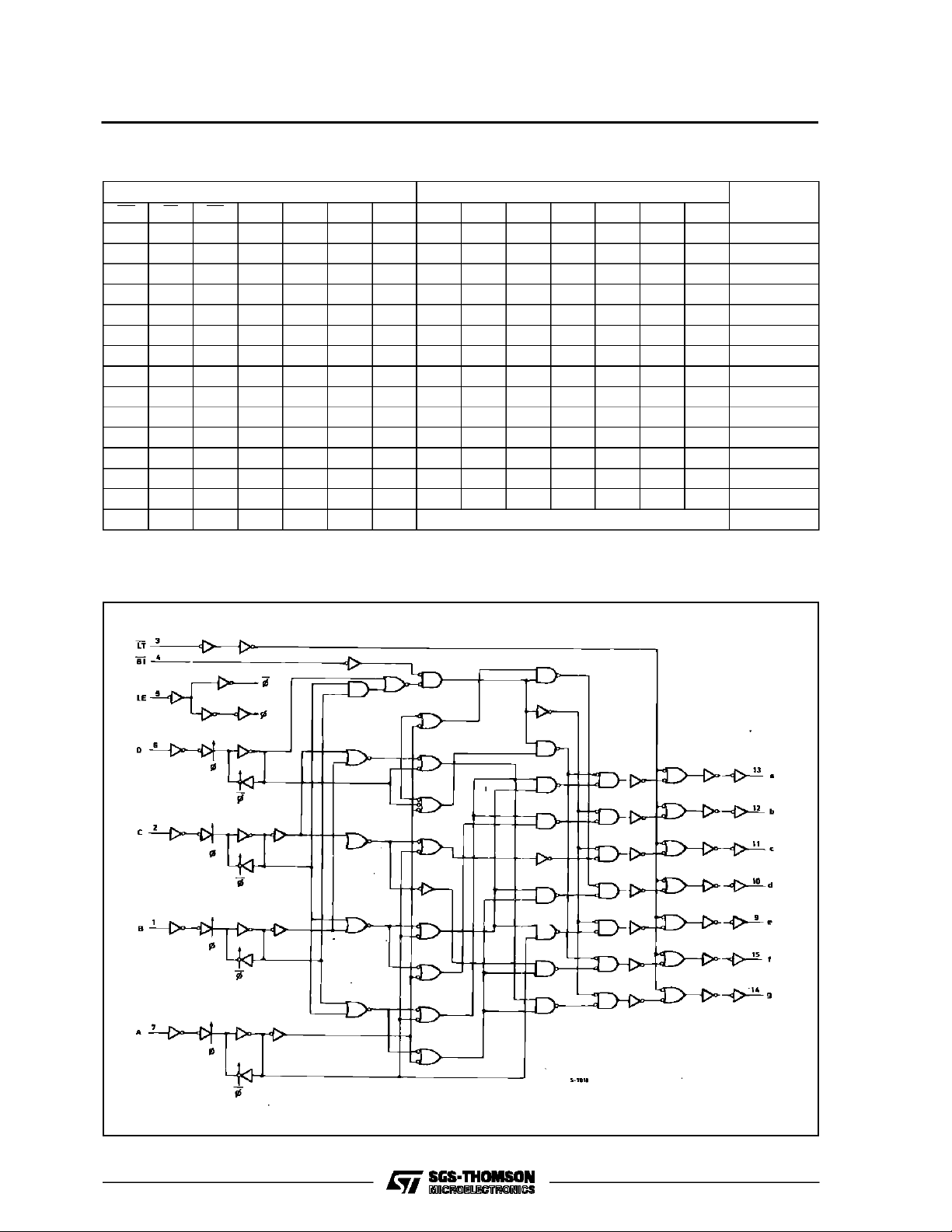
TRUTH TABLE
INPUTS OUTPUTD DISPLAY
LE BI LT D C B A a b c d e f g
XXLXXXXHHHHHHH 8
XLHXXXXLLLLLLL BLANK
LHHLLLLHHHHHHL 0
LHHLLLHLHHLLLL 1
LHHLLHLHHLHHLH 2
LHHLLHHHHHHL LH 3
LHHLHLLLHHLLHH 4
LHHLHLHHLHHLHH 5
LHHLHHLLLHHHHH 6
LHHLHHHHHLLLLL 7
LHHHLLLHHHHHHH 8
LHHHLLHHHHL LHH 9
LHHHLHXLLLLLLL BLANK
LHHHHXXLLLLLLL BLANK
HHHXXXX Hold the stage at the leading edge of LE
X:Don’t Care
MODE
LOGIC DIAGRAM
2/13
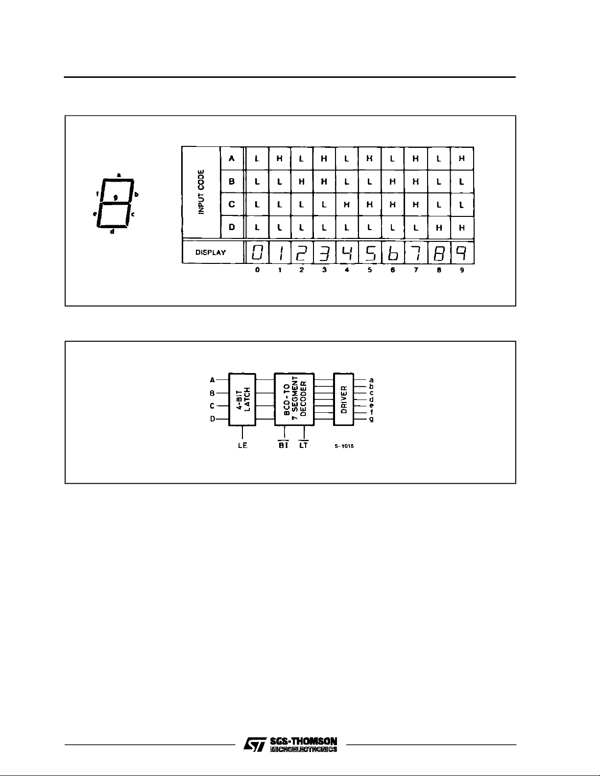
DISPLAY MODE
BLOCK DIAGRAM
M54/M74HC4511
3/13
M54/M74HC4511
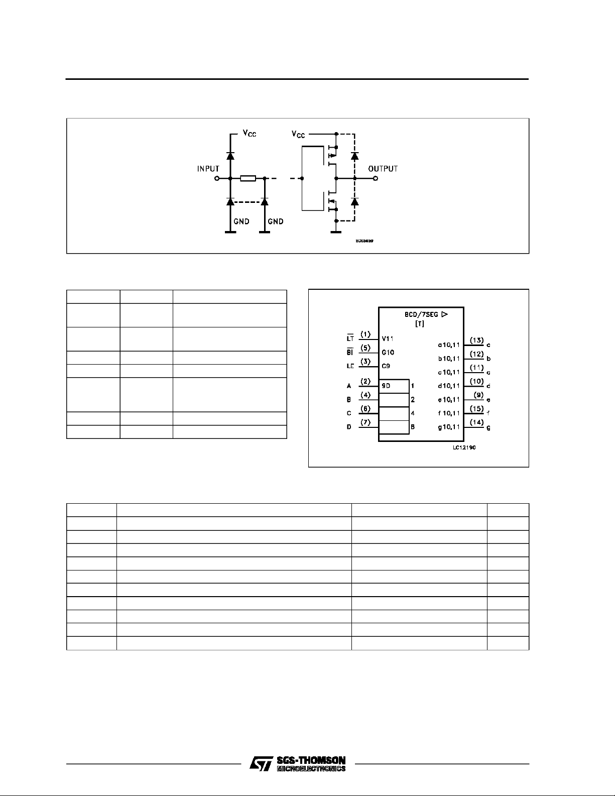
INPUT AND OUTPUT EQUIVALENT CIRCUIT
PIN DESCRIPTION
IEC LOGIC SYMBOL
PIN No SYMBOL NAME AND FUNCTION
3 LT Lamp Test Input (Active
LOW)
4 BI Ripple Blanking Input
(Active LOW)
5 LE Latch Enable Input
7, 1, 2, 6 A to D BCD Address Inputs
13, 12, 11,
a to g Segment Outputs
10, 9 , 15,
14
8 GND Ground (0V)
16 V
CC
Positive Supply Voltage
ABSOLU TE M AXI MU M R AT ING S
Symbol Parameter Value Unit
V
CC
V
V
O
I
IK
I
OK
I
O
I
or I
CC
P
D
T
stg
T
AbsoluteMaximumRatingsarethosevaluesbeyond whichdamagetothedevicemayoccur.Functional operationunder theseconditionisnotimplied.
(*)500 mW:≅ 65oC derateto 300 mWby 10mW/oC: 65oCto85oC
Supply Voltage -0.5 to +7 V
DC Input Voltage -0.5 to VCC+ 0.5 V
I
DC Output Voltage -0.5 to VCC+ 0.5 V
DC Input Diode Current ± 20 mA
DC OutputDiode Current ± 20 mA
DC Output Source Sink Current Per Output Pin -35/25 mA
DC VCCor Ground Current +150/-50 mA
GND
Power Dissipation 500 (*) mW
Storage Temperature -65 to +150
Lead Temperature (10 sec) 300
L
o
C
o
C
4/13
 Loading...