

.HIGH SPEED
tPD= 13 ns(TYP.) AT VCC=5V
.LOW”ON” RESISTANCE:
120 Ω TYP. (VCC-VEE=2V)
50 Ω TYP. (VCC-VEE=4.5 V)
35 Ω TYP. (VCC-VEE=9V)
.WIDEANALOGINPUTVOLTAGERANGE:±6V
.LOW CROSSTALK BETWEEN SWITCHES
.FAST SWITCHING
.SINE WAVE DISTORTION
0.020 (TYP.) AT VCC-VEE=9V
.HIGH NOISEIMMUNITY
V
NIH=VNIL
=28%VCC(MIN.)
.LOW POWER DISSIPATION
ICC=1µA (MAX.) AT VCC5V
.PIN ANDFUNCTION COMPATIBLE
WITH 4316B
M54HC4316
M74HC4316
QUAD BILATERAL SWITCH
B1R
(PlasticPackage)
M1R
(MicroPackage)
ORDER CODES :
M54HC 4316F1R M74H C4316M1R
M74HC 4316B1R M74HC4 316C1R
F1R
(CeramicPackage)
C1R
(Chip Carrier)
DESCRIPTION
The M54/74HC4316 is a high speedCMOS QUAD
BILATERAL SWITCH fabricated in silicon gate
C2MOS technology. It has high speedperformance
combined withtrue CMOSlowpower consumption.
HC4316 has four independent analogue switches.
Each switch has two input/output terminals (nI/O,
nO/I and anactive highselect input (nC).
When the enable input is high all four analog switches are off. The supply voltage for the digital signals applied to VCCand GND must be within the
range 0 to 6 V. The voltage swingon the analogue
Input/Outputs can be between VCC (Positive Limit)
and VEE(Negative Limit).The voltage betweenV
and VEEmustnot exceed 12 V.
All input are equipped with protection circuits
against static discharge and transient excess voltage.
CC
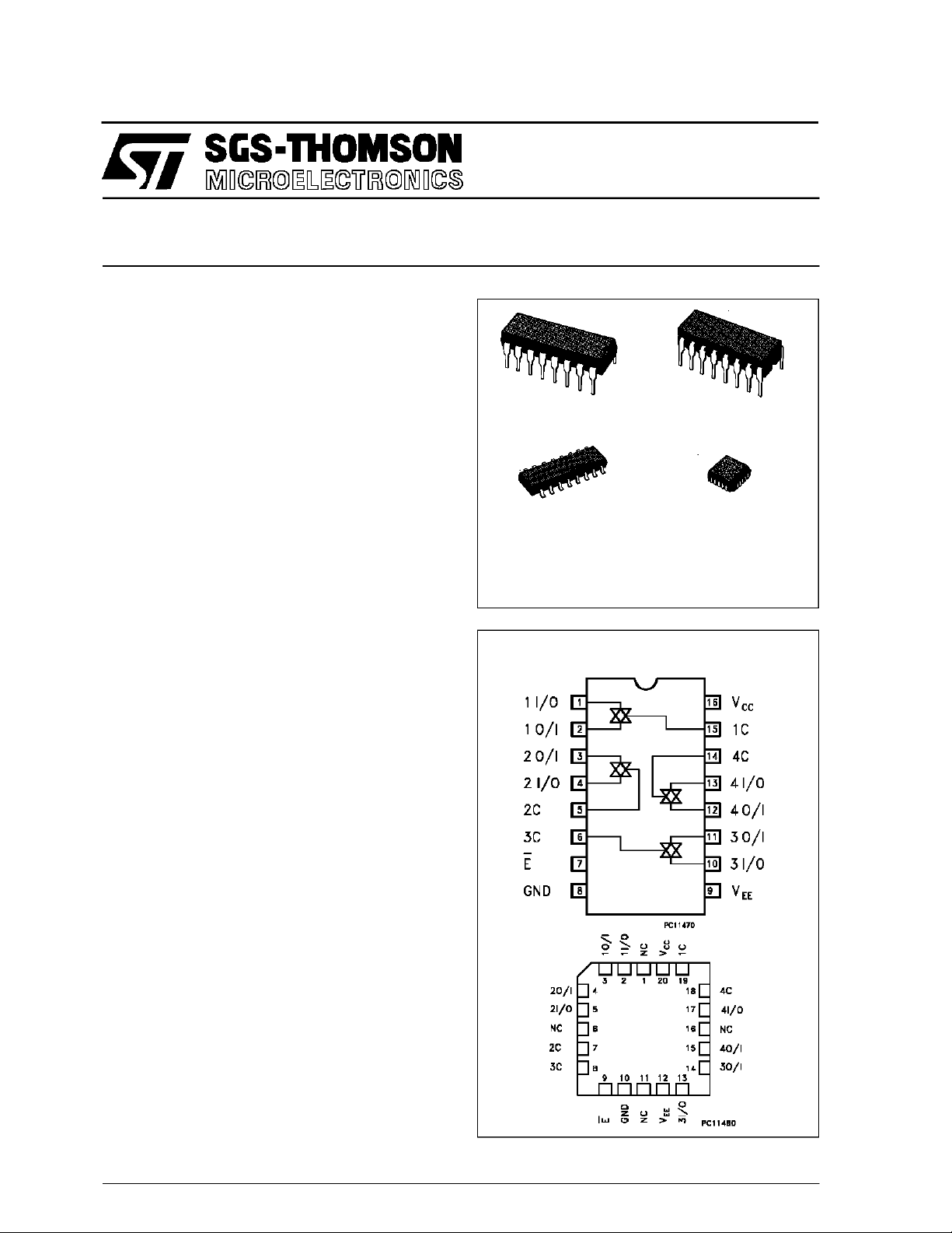
PIN CONNECTIONS(top view)
NC =
No Internal
Connection
October 1993
1/13
M54/M74HC4316
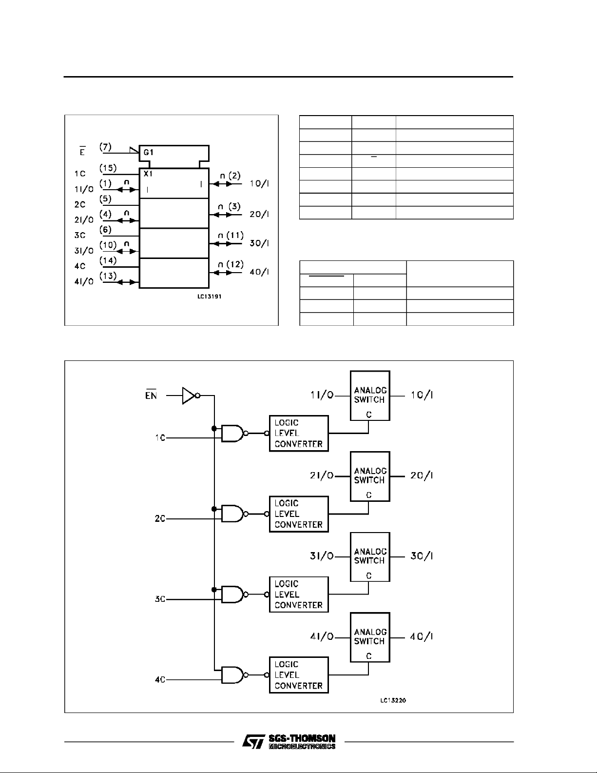
IEC LOGIC SYMBOL PIN DESCRIPTION
PIN No SYMBOL NAME AND FUNCTION
1, 4, 10, 13 1 to 4 I/O Independent Inputs/Outputs
2, 3, 11, 12 1 to 4 O/I Independent Outputs/Inputs
7 E Enable Inputs (Active LOW)
15, 5, 6, 14 1C to 4C Enable Inputs (Active HIGH)
9V
8 GND Ground (0V)
16 V
TRUTH TABLE
EE
CC
Negative Supply Voltage
Positive Supply Voltage
LOGIC DIAGRAM
ENABLE CONTROL
LH ON
L L OFF
H X OFF
SWITCH FUNCTION
2/13
M54/M74HC4316
ABSOLU TE MAXIMU M RAT INGS
Symbol Parameter Value Unit
V
CC
V
CC-VEE
V
V
I/O
I
IK
I
OK
I
O
I
or I
CC
P
D
T
stg
T
L
AbsoluteMaximumRatingsarethose values beyond whichdamage tothedevicemayoccur. Functionaloperationunder theseconditions is notimplied.
(*)500 mW: ≅ 65oC derateto300 mW by 10mW/oC: 65oCto85oC
RECO MM ENDED OPERATI N G CONDI TIONS
Symbol Parameter Value Unit
V
CC
V
EE
V
CC-VEE
V
I
V
I/O
T
op
t
r,tf
Supply Voltage -0.5 to +7 V
Supply Voltage -0.5 to +13 V
C0ntrol Input Voltage -0.5 to VCC+ 0.5 V
I
Switch I/O Voltage VEE-0.5 to VCC+ 0.5 V
DC Input Diode Current ± 20 mA
DC Output Diode Current ± 20 mA
DC Output Source Sink Current Per Output Pin ± 25 mA
DC VCCor Ground Current ± 50 mA
GND
Power Dissipation 500 (*) mW
Storage Temperature -65 to +150
Lead Temperature (10 sec) 300
Supply Voltage 2 to 6 V
Supply Voltage -6 to 0 V
Supply Voltage 2 to 12 V
Input Voltage 0 to V
Switch I/O Voltage VEEto V
Operating Temperature: M54HC Series
M74HC Series
CC
CC
-55 to +125
-40 to +85
Input Rise and Fall Time VCC= 2 V 0 to 1000 ns
= 4.5 V 0 to 500
V
CC
V
= 6 V 0 to 400
CC
o
C
o
C
V
V
o
C
o
C
3/13
M54/M74HC4316
DC SPECIFICATIO NS
Symbol Parameter
V
V
R
∆R
High Level
IHC
Control Input
Voltage
Low Level Control
ILC
Input
Voltage
ON Resistance 4.5 GND VIN=V
ON
Difference of ON
ON
Resistance
Between Switches
Test Conditions Value
V
(V)
CC
V
(V)
EE
=25oC
A
54HC and 74HC
Min. Typ. Max. Min. Max. Min. Max.
-40 to 85oC
74HC
-55 to 125oC
54HC
T
2.0 1.5 1.5 1.5
4.5 3.15 3.15 3.15
6.0 4.2 4.2 4.2
2.0 0.5 0.5 0.5
4.5 1.35 1.35 1.35
6.0 1.8 1.8 1.8
70 170 200
120 180 215
=0.1mA
I/O
V
IN=VIHC
=0.1mA
I/O
IHC
toV
orV
EE
EE
V
4.5 -4.5 50 85 105
6.0 -6.0 30 70 85
I/O=VCC
I
2.0 GND
4.5 GND 50 80 100
4.5 -4.5 35 60 75
V
I/O=VCC
I
6.0 -6.0 20 40 60
4.5 GND VIN=V
4.5 -4.5 5 10 15
6.0 -6.0 5 10 15
V
I/O=VCC
I
I/O
or
IHC
V
ILC
toV
=0.1mA
10 15 20
EE
Unit
V
V
Ω
Ω
I
OFF
I
I
IZ
IN
Input/Output
Leakage Current
(SWITCH OFF)
Switch Input
Leakage Current
(SWITCH ON,
OUTPUT OPEN)
Control Input
Current
6.0 GND VOS=VCCor
GND
VIS=VCCor
6.0 -6.0
GND
V
IN=VIHC
V
or
ILC
6.0 GND VOS=VCCor
GND
6.0 -6.0
6.0
VIN=V
VI=VCCor GND 10-5±0.1 ±1 ±1 µA
or
ILC
V
IHC
±0.06 ±0.6 ±2 µA
±0.1 ±1 ±2
±0.06 ±0.6 ±2 µA
±0.1 ±1 ±2
4/13

AC ELECTRICAL CHARACTERISTICS (CL=50pF,Inputtr=tf=6ns)
Test Conditions Value
T
Symbol Parameter
ø
Phase Difference
I/O
Between Input
and Output
t
t
t
t
PZL
PZH
PLZ
PHZ
Output Enable
Time (E, C-OUT)
Output Disable
Time (E, C-OUT)
Maximum Control
Input Frequency
=25oC
V
(V)
CC
A
54HC and 74HC
Min. Typ. Max. Min. Max. Min. Max.
2.0 GND 12 30 40
4.5 GND 3 6 8
6.0 GND 3 5 7
4.5 -4.5 2 4 5
6.0 -6.0 2 4 5
2.0 GND RL=1KΩ 56 115 145
4.5 GND 14 23 29
6.0 GND 12 20 25
4.5 -4.5 13 21 26
6.0 -6.0 11 18 23
2.0 GND RL=1KΩ 112 205 255
4.5 GND 28 41 51
6.0 GND 24 35 43
4.5 -4.5 24 34 43
6.0 -6.0 21 29 36
2.0 GND R
4.5 GND 9
6.0 GND 11
=1KΩ
L
CL=15pF
V
=
OUT
1/2 V
CC
2
-40 to 85oC
74HC
M54/M74HC4316
-55 to 125oC
54HC
Unit
ns
ns
ns
MHz
C
C
C
C
PD
(*) CPDisdefined as the valueofthe IC’s internalequivalent capacitance which is calculated fromthe operatingcurrentconsumption without load.
(Referto Test Circuit).Average operting current canbe obtainedbythe followingequation. ICC(opr) = CPD•VCC•fIN+I
Input Capacitance 5 10 10 10 pF
IN
Switch Terminal
I/O
Capacitance
Feed Through
IOS
Capacitance
(*) Power Dissipation
4.5 -4.5
4.5 -4.5
5.0 GND 16
5
1
Capacitance
CC
pF
pF
pF
5/13

M54/M74HC4316
ANALO G SWITC H CHAR ACTE R ISTI CS (GND = 0 V TA=25oC)
Test Conditions Value
Symbol Parameter
Sine Wave Distortion
(THD)
f
MAX
Frequency Response
(Switch ON)
Feedthrough
Attenuation (Switch
OFF)
Crosstalk (Control
Input to Signal Output)
Crosstalk (Between
Any Switches)
V
V
(V)
EE
VIN
(Vp-p)
= 1 KHz RL=10Ω CL= 50 pF 0.025
IN
CC
(V)
2.25 2.25 4 f
4.5 4.5 8 0.020
6.0 6.0 11 0.018
2.25 2.25 Adjust fINvoltage to Obtain 0 dBm at VOS.
4.5 4.5 42
6.0 6.0 43
2.25 2.25 V
4.5 4.5 -50
Increase f
RL=50Ω CL=10pF fIN= 1 KHz sine wave
IN
RL= 600 Ω CL=50 pF fIN= 1 MHz sine
6.0 6.0 -50
2.25 2.25 R
4.5 4.5 5
Frequency until dB Meter reads -3dB
IN
is centered at VCC/2. Adjust input for 0 dBm
wave
= 600 Ω CL=50pF
L
fIN= 1 KHz square wave (tr=tf= 6ns) mV
6.0 6.0
2.25 2.25 Adjust V
4.5 4.5 -50
RL= 600 Ω CL=50 pF fIN= 1 MHz sine
6.0 6.0 -50
to Obtain 0 dBm at input
IN
wave
Typ.
Unit
%
28
MHz
-50
dB
-50
dB
6/13

SWITCHING CHARACTERISTICS TEST CIRCUIT
M54/M74HC4316
CONTROL
t
PLZ,tPHZ,tPZL,tPZH
.
CROSSTALK (control to output)
ENABLE
t
PLZ,tPHZ,tPZL,tPZH
.
CROSSTALK BETWEEN ANY TWO
SWITCHES
BANDWIDTHANDFEEDTHROUGH
ATTENUATION
GND (VSS)
C
I–OCI/O
MAXIMUM CONTROL FREQUENCY
GND (VSS)
7/13
M54/M74HC4316
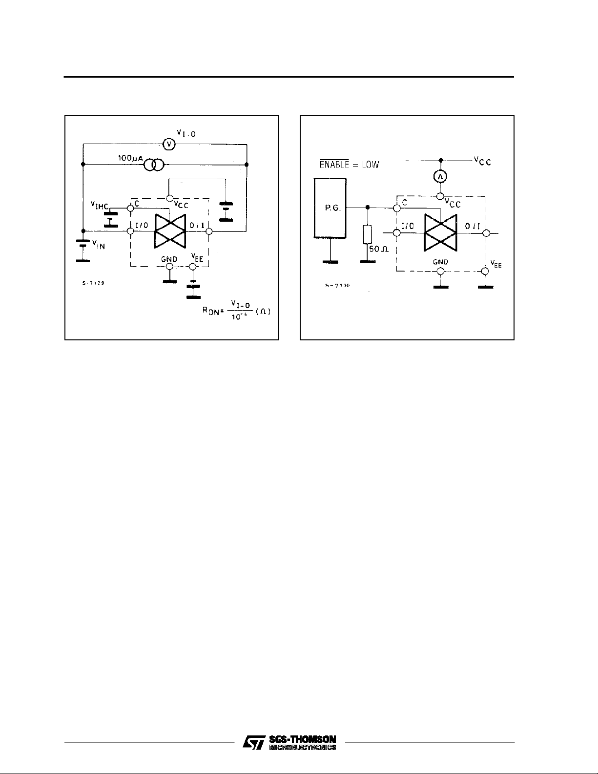
CHANNEL RESISTANCE (RON) ICC(Opr.)
8/13

Plastic DIP14 MECHANICAL DATA
M54/M74HC4316
DIM.
MIN. TYP. MAX. MIN. TYP. MAX.
a1 0.51 0.020
B 1.39 1.65 0.055 0.065
b 0.5 0.020
b1 0.25 0.010
D 20 0.787
E 8.5 0.335
e 2.54 0.100
e3 15.24 0.600
F 7.1 0.280
I 5.1 0.201
L 3.3 0.130
Z 1.27 2.54 0.050 0.100
mm inch
P001A
9/13

M54/M74HC4316
Ceramic DIP14/1 MECHANICAL DATA
DIM.
MIN. TYP. MAX. MIN. TYP. MAX.
A 20 0.787
B 7.0 0.276
D 3.3 0.130
E 0.38 0.015
e3 15.24 0.600
F 2.29 2.79 0.090 0.110
G 0.4 0.55 0.016 0.022
H 1.17 1.52 0.046 0.060
L 0.22 0.31 0.009 0.012
M 1.52 2.54 0.060 0.100
N 10.3 0.406
P 7.8 8.05 0.307 0.317
Q 5.08 0.200
mm inch
10/13
P053C

SO14 MECHANICAL DATA
M54/M74HC4316
DIM.
MIN. TYP. MAX. MIN. TYP. MAX.
A 1.75 0.068
a1 0.1 0.2 0.003 0.007
a2 1.65 0.064
b 0.35 0.46 0.013 0.018
b1 0.19 0.25 0.007 0.010
C 0.5 0.019
c1 45° (typ.)
D 8.55 8.75 0.336 0.344
E 5.8 6.2 0.228 0.244
e 1.27 0.050
e3 7.62 0.300
F 3.8 4.0 0.149 0.157
G 4.6 5.3 0.181 0.208
L 0.5 1.27 0.019 0.050
M 0.68 0.026
S8°(max.)
mm inch
P013G
11/13

M54/M74HC4316
PLCC20 MECHANICAL DATA
DIM.
MIN. TYP. MAX. MIN. TYP. MAX.
A 9.78 10.03 0.385 0.395
B 8.89 9.04 0.350 0.356
D 4.2 4.57 0.165 0.180
d1 2.54 0.100
d2 0.56 0.022
E 7.37 8.38 0.290 0.330
e 1.27 0.050
e3 5.08 0.200
F 0.38 0.015
G 0.101 0.004
M 1.27 0.050
M1 1.14 0.045
mm inch
12/13
P027A

M54/M74HC4316
Information furnishedis believed to be accurate and reliable. However, SGS-THOMSON Microelectronicsassumes no responsability for the
consequences of useof suchinformation nor forany infringement ofpatents or other rights of third parties which may results from its use. No
license is granted byimplication or otherwiseunder any patentor patent rights ofSGS-THOMSON Microelectronics. Specificationsmentioned
in this publication are subjectto changewithout notice. This publication supersedes andreplaces all information previously supplied.
SGS-THOMSON Microelectronicsproducts are not authorized foruse ascritical componentsinlife supportdevices or systemswithout express
written approval of SGS-THOMSON Microelectonics.
1994SGS-THOMSON Microelectronics- All RightsReserved
Australia -Brazil - France - Germany - Hong Kong - Italy - Japan - Korea - Malaysia - Malta -Morocco - The Netherlands-
Singapore -Spain - Sweden- Switzerland - Taiwan - Thailand- UnitedKingdom - U.S.A
SGS-THOMSON Microelectronics GROUP OFCOMPANIES
13/13
 Loading...