

SGS Thomson Microelectronics M74HC423, M74HC423A Datasheet
M54HC423/423A
M74HC423/423A
DUAL RETRIGGERABLE MONOSTABLE MULTIVIBRATOR
.HIGH SPEED
tPD= 25 ns(TYP) at VCC=5V
.LOWPOWERDISSIPATION
STANDBYSTATEICC=4µA (MAX.)AT TA=25°C
ACTIVESTATEICC=700µA (MAX.)ATVCC=5V
.HIGH NOISE IMMUNITY
V
NIH=VNIL
.OUTPUT DRIVE CAPABILITY
10 LSTTL LOADS
=28%VCC(MIN.)
B1R
(PlasticPackage)
(CeramicPackage)
.SYMMETRICALOUTPUT IMPEDANCE
IOH=IOL= 4 mA (MIN.)
.BALANCEDPROPAGATION DELAYS
t
PLH=tPHL
.WIDE OPERATINGVOLTAGERANGE
VCC(OPR)= 2V TO6 V
.WIDE OUTPUT PULSE WIDTHRANGE
t
=120ns ∼ 60 s OVER AT VCC= 4.5 V
WOUT
M1R
(MicroPackage)
ORDER CODES :
M54HC X XXF1R M74H CXXXM1R
M74HC X XXB1R M74HCX X XC1R
(Chip Carrier)
.PIN AND FUNCTION COMPATIBLE WITH
54/74LS423
F1R
C1R
DESCRIPTION
The M54/74HC423/423A are high speed CMOS
MONOSTABLE multivibrators fabricated with
silicongate C2MOS technology.
They achieve the high speed operation similar to
equivalent LSTTL whilemaintaining the CMOSlow
power dissipation. There are two trigger inputs, A
INPUT (negative edge) and B INPUT (positive
edge). These inputs are valid for rising/falling
signals, (tr–tf– 1 sec). After triggering the output
maintains the MONOSTABLE state for the time
period determined by the external resistor Rx and
capacitor Cx.
Two different pulse width constant are available:
K ≅ 0.46 for HC423 K ≅ 1 for HC423A.
Taking CLR low breaks this MONOSTABLE
STATE. If the next trigger pulse occurs during the
MONOSTABLEperiodit makestheMONOSTABLE
periodlonger. Limit for values ofCx and Rx :
Cx : NO LIMIT
Rx : VCC<3.0 V 5K Ω to1 M Ω
VCC≥ 3.0 V 1 K Ω to 1 M Ω
All inputs are equipped with protection circuits
against static discharge and transient excess
voltage.
PIN CONNECTIONS(top view)
NC =
No Internal
Connection
October 1993
1/14
M54/M74HC423/423A
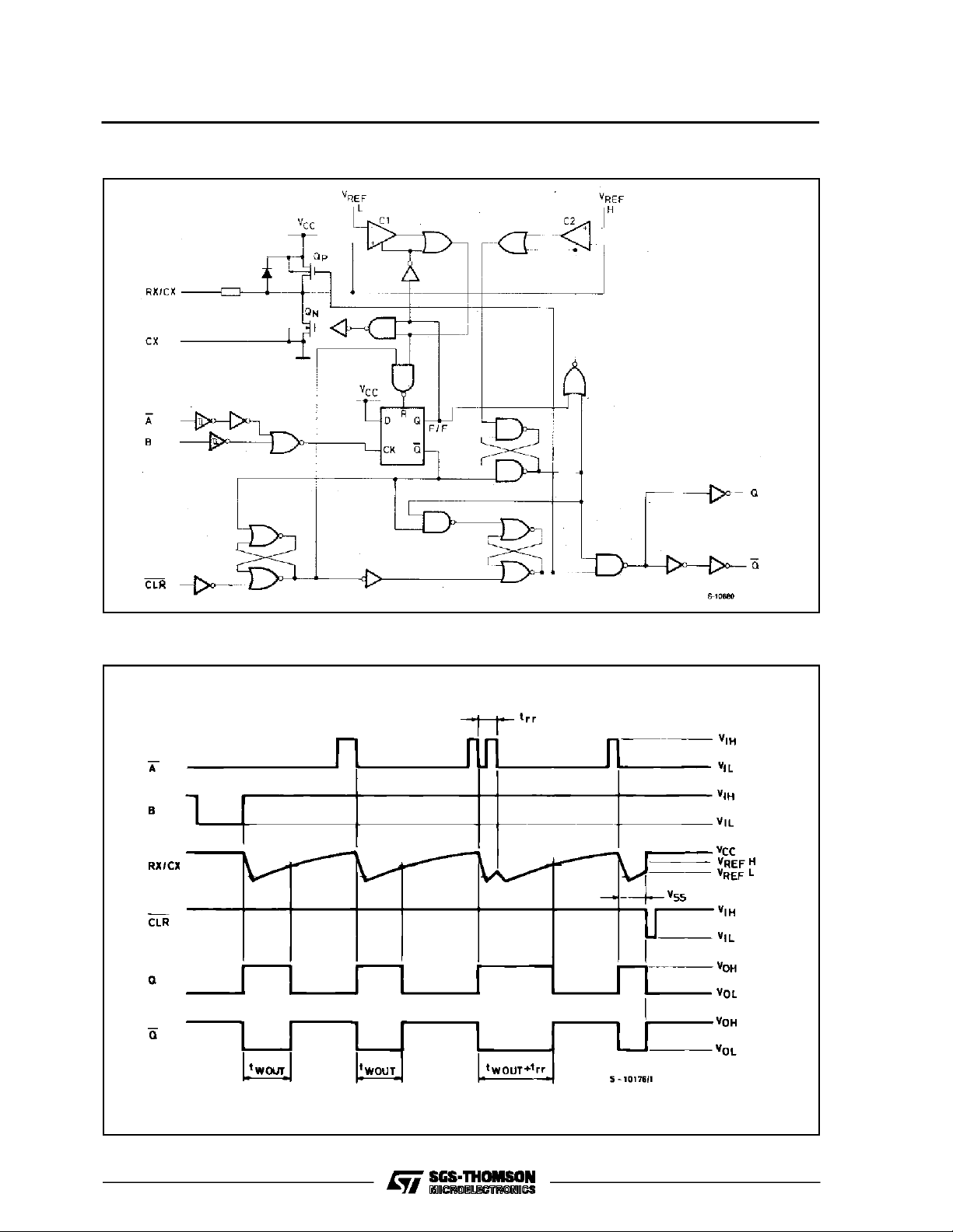
SYSTEM DIAGRAM
TIMING CHART
2/14
M54 / M74HC4 23 /423 A
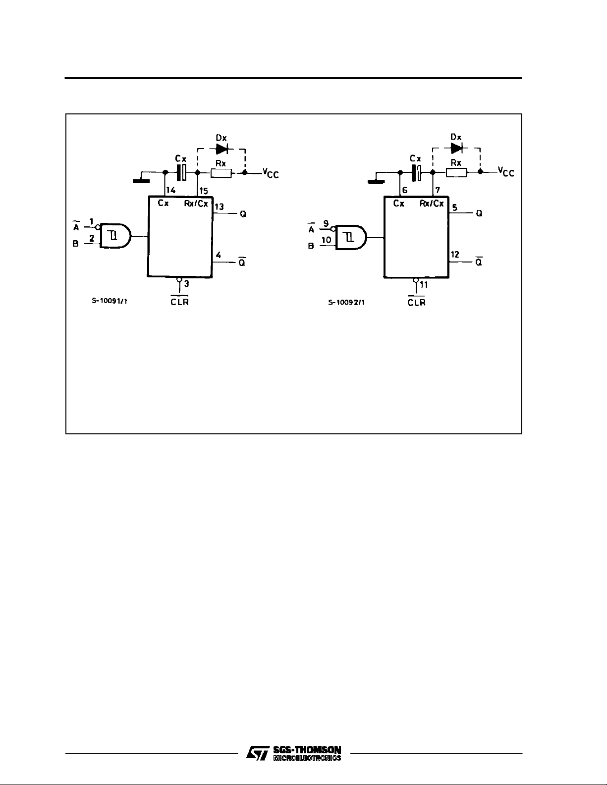
BLOCK DIAGRAM
Note:
(1)Cx, Rx, Dx are externalcomponents.
(2)Dx isa clampingdiode.
Theexternalcapacitor ischarged toVCCinthestand-by state,i.e.notrigger.Whenthesupply voltageis turned offCxis dischargedmainly
throughan internalparasiticdiode (see figures). IfCx issufficientlylarge and VCCdecreases rapidy,therewill besomepossibility of damagingtheI.C.witha surgecurrentor latch-up. If the voltagesupply filtercapacitor is largeenough and VCCdecrease slowly,the surge
currentis automaticallylimitedand damage the I.C. is avoided. Themaximumforwardcurrentof the parasiticdiodeisapproximately 20
mA.In caseswhereCx is large the timetakenfor the supply voltageto fallto 0.4VCCcanbecalculated asfollows:
tf≥ (VCC–0.7)⋅Cx/20mA
Incases wheretfistoo short anexternal clampingdiode is required toprotect theI.C.fromthe surge current.
FUNCTIONAL DESCRIPTION
STAND-BYSTATE
The external capacitor, Cx, is fully charged to V
CC
in the stand-by state. Hence, before triggering,
transistorQpandQn(connected tothe Rx/Cxnode)
are both turned-off. The two comparators that
control the timing and the two reference voltage
sources stop operating. The total supply current is
therefore only leakage current.
TRIGGEROPERATION
Triggering occurswhen :
1 st) A is”low” andB hasa falling edge ;
2 nd) B is ”high”and Ahas a rising edge;
3 rd) AislowandB ishighand C1hasa risingedge.
After the multivibrator has been retriggered
comparator C1 and C2 start operating and Qn is
turned on. Cx then discharges through Qn. The
voltage at the node R/C external falls.
When itreaches V
theoutputof comparatorC1
REFL
becomeslow.Thisinturnresets theflip-flop andQn
is turned off.
At this pointC1 stopsfunctioning but C2 continues
to operate.
ThevoltageatR/Cexternalbeginstorisewithatime
constantset by the externalcomponents Rx, Cx.
Triggering themultivibratorcausesQto gohighafter
internal delay due to the flip-flop and the gate. Q
remains highuntil the voltage at R/C external rises
againto V
. AtthispointC2outputgoeslow and
REFH
O goes low. C2 stop operating. That means that
after triggering when the voltage R/C external
returns toV
themultivibratorhas returned toits
REFH
MONOSTABLESTATE. In the case whereRx ⋅ Cx
are large enough and the discharge time of the
capacitor and the delay time in the I.C. can be
ignored, the width of the outputpulse tw (out) is as
follows :
t
W(OUT)
= 0.46 Cx ⋅ Rx (HC423)
t
W(OUT)
=Cx⋅Rx (HC423A)
3/14
M54/M74HC423/423A
FUNCTIONAL DESCRIPTION (continued)
RE-TRIGGEREDOPERATION
When a second trigger pulse follows the first its
effect willdepend onthe state ofthe multivibrator. If
the capacitor Cx is being charged the voltage level
of R/C external falls to Vrefl again and Q remains
high i.e.the retrigger pulse arrives in atimeshorter
than the period Rx ⋅ Cx seconds, the capacitor
charging time constant.If the second trigger pulse
is verycloseto theinitialtrigger pulseitisineffective
; i.e. thesecond triggermust arrive in the capacitor
minimum time for a second trigger to be effective
depends on VCCandCx.
RESETOPERATION
CL is normally high. If CL is low, the trigger is not
effective because Q output goes low and trigger
control flip-flopis reset.
Also transistor Op is turned on and Cx is charged
quickyto VCC. Thismeans if CL inputgoes low,the
IC becomeswaiting state both inoperating andnon
operating state.
discharge cycle to be ineffective; Hence the
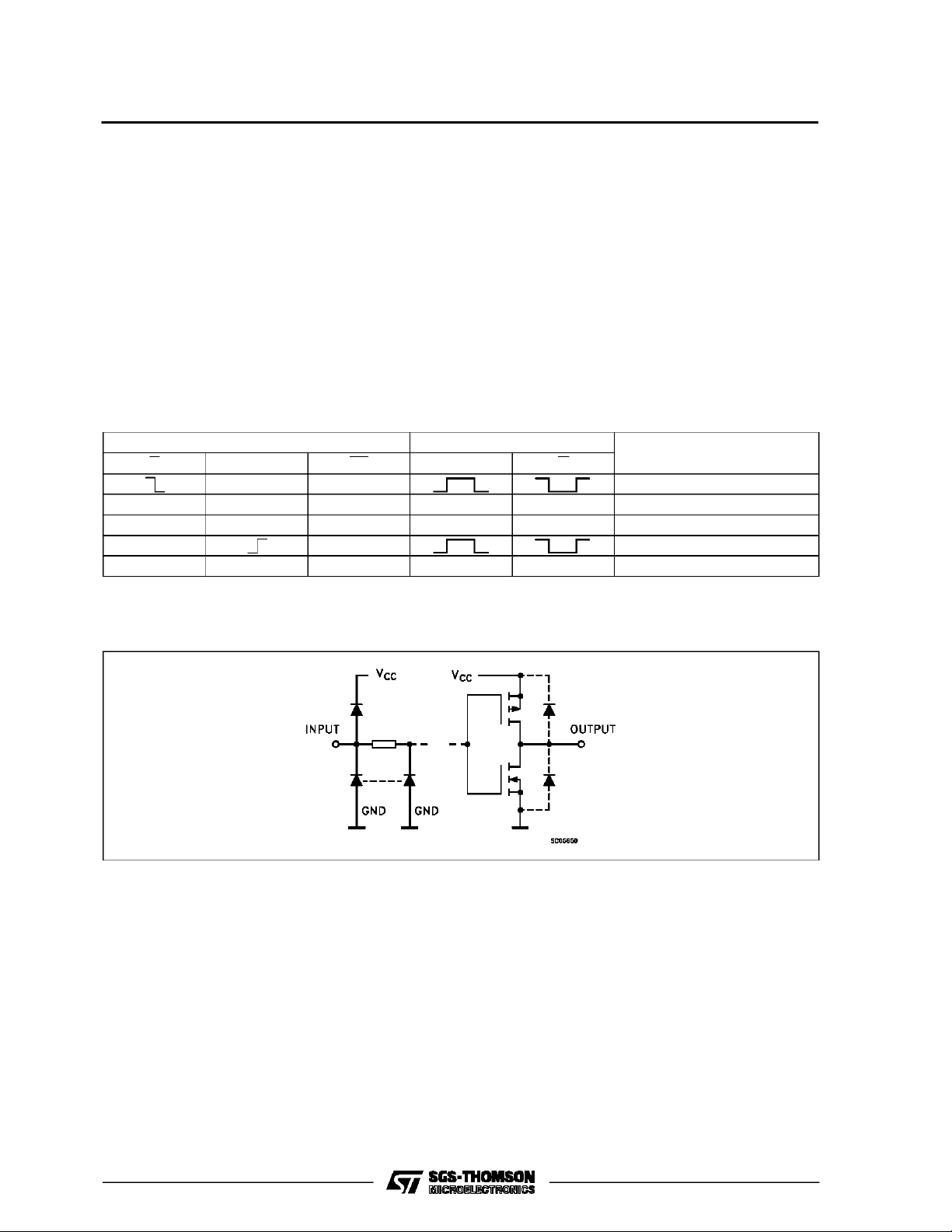
TRUTH TABLE
INPUTS OUTPUTS
ABCLQQ
H H OUTPUT ENABLE
X L H L H INHIBIT
H X H L H INHIBIT
L H OUTPUT ENABLE
X X L L H INHIBIT
X:Don’t Care Z:HighImpedance
NOTE
INPUT AND OUTPUT EQUIVALENT CIRCUIT
4/14
M54 / M74HC4 23 /423 A
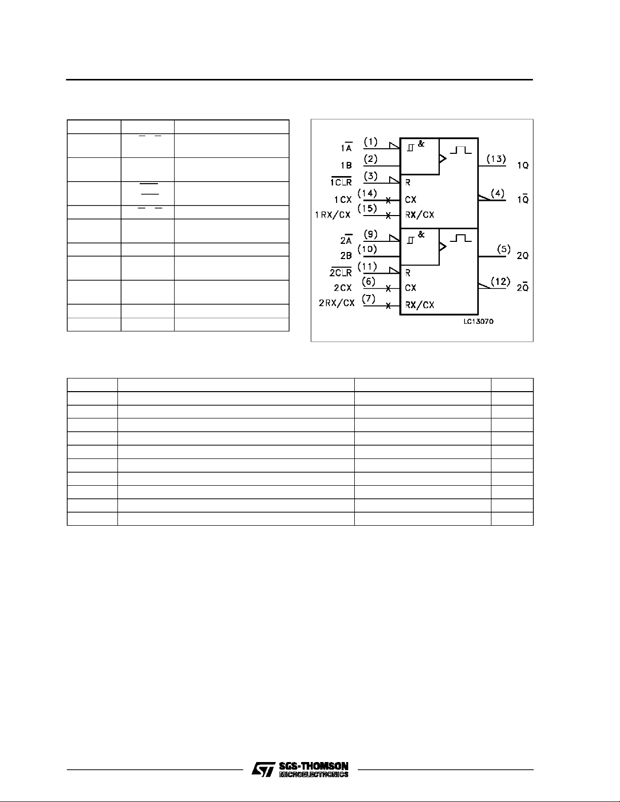
PIN DESCRIPTION
IEC LOGIC SYMBOL
PIN No SYMBOL NAME AND FUNCTION
1, 9 1A, 2A Trigger Inputs (Negative
Edge Triggered)
2, 10 1B, 2B Trigger Inputs (Positive
Edge Triggered)
3, 11 1CLR,
Direct Reset (Active LOW)
2CLR
4, 12 1Q, 2Q Outputs (Active LOW)
72R
EXT/CEXT
External Resistor
Capacitor Connection
13, 5 1Q, 2Q Outputs (Active HIGH)
14, 6 1C
2C
15 1R
EXT/CEXT
EXT
EXT
External Capacitor
Connection
External Resistor
Capacitor Connection
8 GND Ground (0V)
16 V
CC
Positive Supply Voltage
ABSOLU TE M AXIMU M R AT ING
Symbol Parameter Value Unit
V
CC
V
V
O
I
IK
I
OK
I
O
I
or I
CC
P
D
T
stg
T
AbsoluteMaximumRatingsarethosevalues beyondwhichdamagetothedevicemayoccur.Functionaloperationunderthesecondition isnotimplied.
(*)500 mW: ≅ 65oC derateto300mW by 10mW/oC: 65oCto85oC
Supply Voltage -0.5 to +7 V
DC Input Voltage -0.5 to VCC+ 0.5 V
I
DC Output Voltage -0.5 to VCC+ 0.5 V
DC Input Diode Current ± 20 mA
DC Output Diode Current ± 20 mA
DC Output Source Sink Current Per Output Pin ± 25 mA
DC VCCor Ground Current ± 50 mA
GND
Power Dissipation 500 (*) mW
Storage Temperature -65 to +150
Lead Temperature (10 sec) 300
L
o
C
o
C
5/14
 Loading...