

8 BIT SIPOSHIFT LATCH REGISTER (3-STATE)
.HIGH SPEED
f
= 73 MHz (TYP.) AT VCC=5V
MAX
.LOWPOWER DISSIPATION
ICC=4µA(MAX.) AT TA=25°C
.HIGH NOISE IMMUNITY
V
NIH=VNIL
=28%VCC(MIN.)
.OUTPUT DRIVE CAPABILITY
10 LSTTL LOADS
.SYMMETRICALOUTPUT IMPEDANCE
|IOH|=IOL=4 mA (MIN.)
.BALANCEDPROPAGATION DELAYS
t
PLH=tPHL
.WIDE OPERATING VOLTAGERANGE
VCC(OPR)= 2 V TO 6 V
.PIN AND FUNCTION COMPATIBLE
WITH 4094B
M54HC4094
M74HC4094
B1R
(PlasticPackage)
M1R
(MicroPackage)
ORDER CODES :
M54HC 4094F1R M74H C4094M1R
M74HC 4094B1R M74HC4 094C1R
F1R
(CeramicPackage)
C1R
(Chip Carrier)
DESCRIPTION
The M54/74HC4094 is a high speed CMOS 8 BIT
SIPOSHIFTLATCH REGISTERfabricatedwithsilicon gate C2MOS technology.
It has the same high speed performance of LSTTL
combined withtrue CMOSlow power consumption.
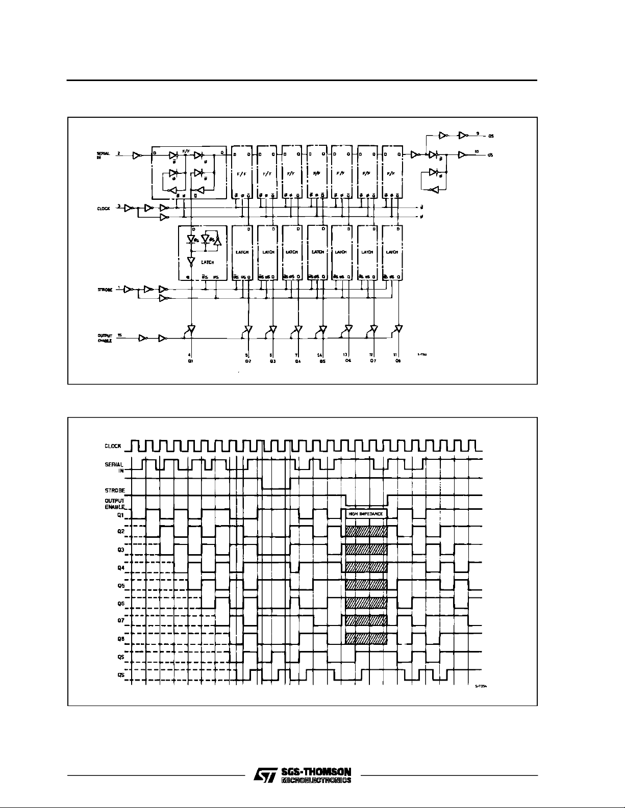
This deviceconsists of an 8-bit shiftregister and an
8-bit latch with 3-state output buffer.Data is shifted
serially through the shift register on the positive
going transition of the clockinput signal.Theoutput
of the last stage (Qs) can be used to cascadeseveraldevices.
DataontheQs outputistransferredtoa secondoutput (Qs’) on the following negative transition of the
clockinputsignal. Thedataof eachstageoftheshift
register is provided with a latch,which latches data
on the negative going transition of the STROBE
inputsignal. When the STROBE input is held high,
datapropagatesthroughthelatchtoa3-stateoutput
buffer.
This buffer is enabled when OUTPUT ENABLE
inputistakenhigh. Allinputsare equipped with protectioncircuitsagainststaticdischarge andtransient
excess voltage.
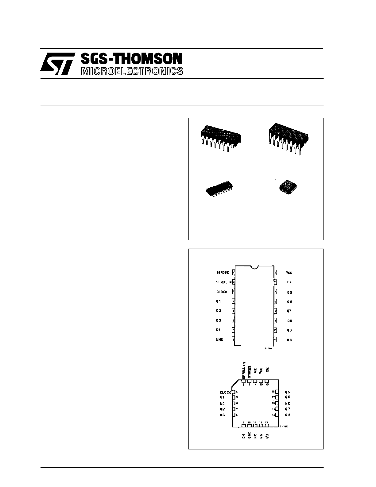
PIN CONNECTIONS (top view)
NC =
No Internal
Connection
February 1993
1/12
M54/M74HC4094
LOGIC DIAGRAM
LOGIC DIAGRAM
2/12
TRUTH TABLE
M54/M74HC4094
CK OE ST SI
H H L L Qn-1 Q7 NC
H H H H Qn-1 Q7 NC
H L X NCNCQ7NC
LXXZZQ7NC
HXXNCNCNCQs
LXXZZNCQs
X:Don’tCare Z: HighImpedance NC:NoChange
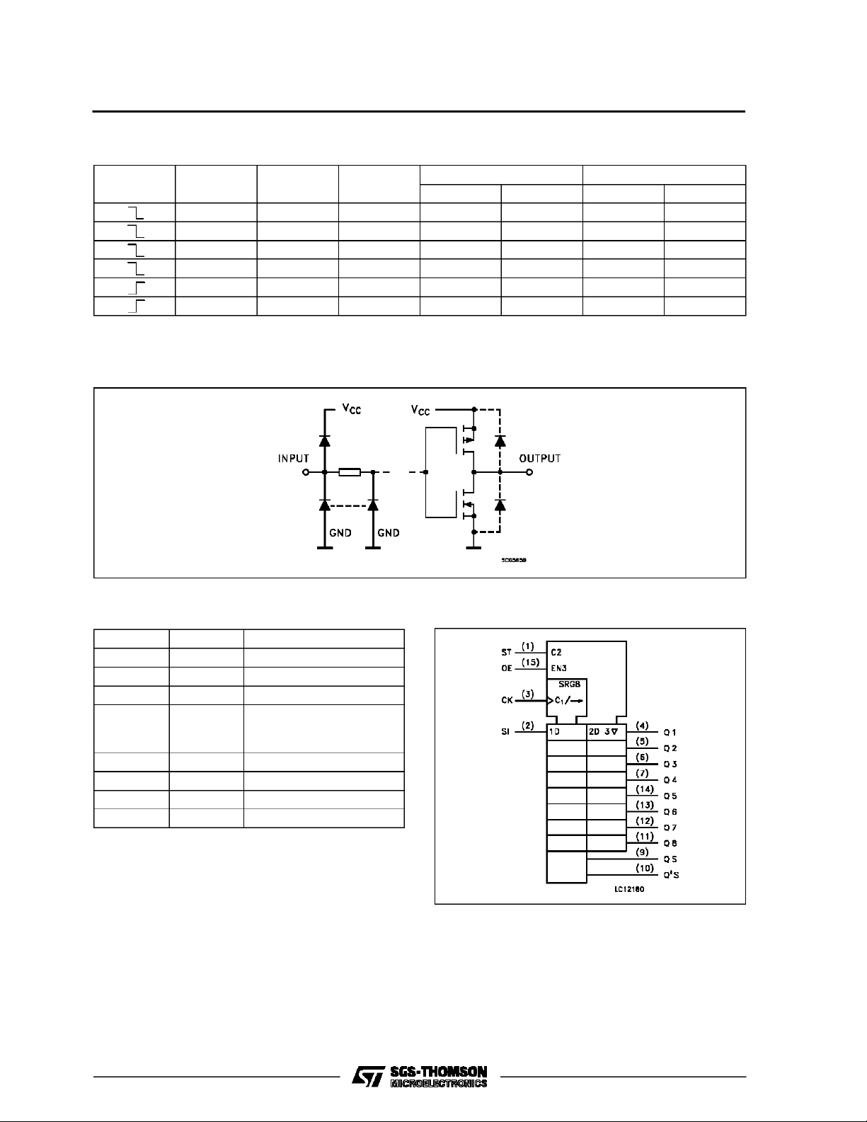
INPUT AND OUTPUT EQUIVALENT CIRCUIT
PARALLEL OUTPUT SERIAL OUTPUT
Q1 Qn Qs Qs’
PIN DESCRIPTION
PIN No SYMBOL NAME AND FUNCTION
1 STROBE Strobe Input
2 SERIAL IN Serial Input
3 CLOCK Clock Input
4, 5, 6, 7,
14, 13, 12,
11
9, 10 QS Q’S Serial Outputs
15 OE Output Enable Input
8 GND Ground (0V)
16 V
Q1 to Q7 Parallel Outputs
CC
Positive Supply Voltage
IEC LOGIC SYMBOL
3/12
M54/M74HC4094
ABSOLU TE M AXIMU M R AT INGS
Symbol Parameter Value Unit
V
CC
V
V
O
I
IK
I
OK
I
O
I
or I
CC
P
D
T
stg
T
AbsoluteMaximumRatingsarethosevalues beyond whichdamagetothedevicemayoccur.Functionaloperationunder these conditionisnotimplied.
(*)500 mW:≅ 65oC derateto300mWby 10mW/oC: 65oCto85oC
RECO MM ENDED OPERAT I N G C ONDITI ONS
Symbol Parameter Value Unit
V
CC
V
I
V
O
T
op
t
r,tf
Supply Voltage -0.5 to +7 V
DC Input Voltage -0.5 to VCC+ 0.5 V
I
DC Output Voltage -0.5 to VCC+ 0.5 V
DC Input Diode Current ± 20 mA
DC Output Diode Current ± 20 mA
DC Output Source Sink Current Per Output Pin ± 25 mA
DC VCCor Ground Current ± 50 mA
GND
Power Dissipation 500 (*) mW
Storage Temperature -65 to +150
Lead Temperature (10 sec) 300
L
Supply Voltage 2 to 6 V
Input Voltage 0 to V
Output Voltage 0 to V
Operating Temperature: M54HC Series
M74HC Series
CC
CC
-55 to +125
-40 to +85
Input Rise and Fall Time VCC= 2 V 0 to 1000 ns
V
= 4.5 V 0 to 500
CC
V
= 6 V 0 to 400
CC
o
C
o
C
V
V
o
C
o
C
4/12

DC SPECIFICATIONS
Symbol Parameter
V
V
V
V
I
I
High Level Input
IH
Voltage
Low Level Input
IL
Voltage
High Level
OH
Output Voltage
Low Level Output
OL
Voltage
I
Input Leakage
I
Current
3 State Output
OZ
Off State Current
Quiescent Supply
CC
Current
M54/M74HC4094
Test Conditions Value
T
=25oC
V
(V)
CC
A
54HC and 74HC
Min. Typ. Max. Min. Max. Min. Max.
2.0 1.5 1.5 1.5
4.5 3.15 3.15 3.15
6.0 4.2 4.2 4.2
2.0 0.5 0.5 0.5
4.5 1.35 1.35 1.35
6.0 1.8 1.8 1.8
2.0
4.5 4.4 4.5 4.4 4.4
6.0 5.9 6.0 5.9 5.9
4.5 I
6.0 I
2.0
4.5 0.0 0.1 0.1 0.1
6.0 0.0 0.1 0.1 0.1
4.5 I
6.0 I
6.0
=
V
I
IO=-20 µA
V
IH
or
V
IL
=-4.0 mA 4.18 4.31 4.13 4.10
O
=-5.2 mA 5.68 5.8 5.63 5.60
O
V
=
I
IO=20µA
V
IH
or
V
IL
= 4.0 mA 0.17 0.26 0.37 0.40
O
= 5.2 mA 0.18 0.26 0.37 0.40
O
VI=VCCor GND ±0.1 ±1 ±1 µA
6.0 VI=VIHor V
1.9 2.0 1.9 1.9
0.0 0.1 0.1 0.1
IL
VO=VCCor GND
6.0 VI=VCCor GND 4 40 80 µA
-40 to 85oC
74HC
-55 to 125oC
54HC
Unit
±0.5 ±5.0 ±10 µA
V
V
V
V
5/12

M54/M74HC4094
AC ELECTRICAL CHARACTERISTICS (CL=50pF,Inputtr=tf=6ns)
Test Conditions Value
T
=25oC
Symbol Parameter
t
t
TLH
THL
Output Transition
Time
V
CC
(V)
2.0 30 75 95 110
4.5 8151922
A
54HC and 74HC
Min. Typ. Max. Min. Max. Min. Max.
6.0 7131619
t
PLH
t
PHL
Propagation
Delay Time
(CLOCK - Qn)
t
t
PLH
PHL
Propagation
Delay Time
(C LOCK-QS ,Q’S)
t
t
PLH
PHL
Propagation
Delay Time
(STROBE - Qn)
t
t
PZL
PZH
3 State Output
Enable Time
2.0 92 200 250 300
4.5 26 40 50 60
6.0 20 34 43 51
2.0 65 150 190 225
4.5 19 30 38 45
6.0 15 26 32 38
2.0 75 160 200 240
4.5 20 32 40 48
6.0 16 27 34 41
2.0 58 150 190 225
4.5 16 30 38 45
6.0 13 26 32 38
t
t
PHZ
PLZ
3 State Output
Disable Time
2.0 35 150 190 225
4.5 16 30 38 45
6.0 13 26 32 38
f
MAX
Maximum Clock
Frequency
2.0 6 16 4.8 4
4.5 30 66 24 20
6.0 35 80 28 24
t
W(H)
t
W(L)
Minimum Pulse
Width
2.0 17 75 95 110
4.5 7151922
6.0 6131619
t
W(L)
Minimum Pulse
Width
2.0 28 75 95 110
4.5 6151922
6.0 6131619
Minimum Set-up
t
s
Time
(SI)
Minimum Set-up
t
s
Time
(ST)
t
Minimum Hold
h
Time
(SI, ST)
C
C
PD
Input Capacitance 5 10 10 10 pF
IN
(*) Power Dissipation
2.0 30 75 95 110
4.5 7151922
6.0 5131619
2.0 45 100 125 145
4.5 10 20 25 29
6.0 8172125
2.0 0 0 0
4.5 0 0 0
6.0 0 0 0
140
Capacitance
(*) CPDisdefined as the valueofthe IC’s internal equivalent capacitance whichis calculated fromthe operating current consumption withoutload.
(RefertoTest Circuit).Average opertingcurrentcanbe obtained bythefollowingequation. ICC(opr) = CPD•VCC•fIN+ICC/2(per FLIP/FLOP)
-40 to 85oC
74HC
-55 to 125oC
54HC
Unit
ns
ns
ns
ns
ns
ns
MHz
ns
ns
ns
ns
ns
pF
6/12

SWITCHING CHARACTERISTICS TEST WAVEFORM
M54/M74HC4094
TEST WAVEFORM ICC(Opr.)
CPDCALCULATION
CPDis tobe calculatedwith thefollowing formula by using the measured value of I
(Opr.)in the test circuitopposite.
I
(
Opr
CPD=
f
CC
IN
)
×
V
CC
In determining the typical value of CPD,a
relatively high frequency of 1 MHz was applied to fIN, in order to eliminate any error
caused by thequiescent supply current.
CC
7/12

M54/M74HC4094
Plastic DIP16 (0.25) MECHANICAL DATA
DIM.
MIN. TYP. MAX. MIN. TYP. MAX.
a1 0.51 0.020
B 0.77 1.65 0.030 0.065
b 0.5 0.020
b1 0.25 0.010
D 20 0.787
E 8.5 0.335
e 2.54 0.100
e3 17.78 0.700
F 7.1 0.280
I 5.1 0.201
L 3.3 0.130
Z 1.27 0.050
mm inch
8/12
P001C

Ceramic DIP16/1 MECHANICAL DATA
M54/M74HC4094
DIM.
MIN. TYP. MAX. MIN. TYP. MAX.
A 20 0.787
B 7 0.276
D 3.3 0.130
E 0.38 0.015
e3 17.78 0.700
F 2.29 2.79 0.090 0.110
G 0.4 0.55 0.016 0.022
H 1.17 1.52 0.046 0.060
L 0.22 0.31 0.009 0.012
M 0.51 1.27 0.020 0.050
N 10.3 0.406
P 7.8 8.05 0.307 0.317
Q 5.08 0.200
mm inch
P053D
9/12

M54/M74HC4094
SO16 (Narrow) MECHANICAL DATA
DIM.
MIN. TYP. MAX. MIN. TYP. MAX.
A 1.75 0.068
a1 0.1 0.2 0.004 0.007
a2 1.65 0.064
b 0.35 0.46 0.013 0.018
b1 0.19 0.25 0.007 0.010
C 0.5 0.019
c1 45° (typ.)
D 9.8 10 0.385 0.393
E 5.8 6.2 0.228 0.244
e 1.27 0.050
e3 8.89 0.350
F 3.8 4.0 0.149 0.157
G 4.6 5.3 0.181 0.208
L 0.5 1.27 0.019 0.050
M 0.62 0.024
S8°(max.)
mm inch
10/12
P013H

PLCC20 MECHANICAL DATA
M54/M74HC4094
DIM.
MIN. TYP. MAX. MIN. TYP. MAX.
A 9.78 10.03 0.385 0.395
B 8.89 9.04 0.350 0.356
D 4.2 4.57 0.165 0.180
d1 2.54 0.100
d2 0.56 0.022
E 7.37 8.38 0.290 0.330
e 1.27 0.050
e3 5.08 0.200
F 0.38 0.015
G 0.101 0.004
M 1.27 0.050
M1 1.14 0.045
mm inch
P027A
11/12

M54/M74HC4094
Information furnished is believed to be accurate and reliable. However, SGS-THOMSON Microelectronics assumes no responsability for the
consequences of use of such information nor for any infringement of patents or other rights of third parties which may results from its use. No
license is granted byimplication or otherwise under any patent or patentrights of SGS-THOMSON Microelectronics. Specificationsmentioned
in this publication are subject to change without notice. This publication supersedes and replaces all information previously supplied.
SGS-THOMSON Microelectronicsproducts are not authorized foruse ascritical componentsin life support devices or systems without express
written approval of SGS-THOMSON Microelectonics.
1994 SGS-THOMSON Microelectronics - All Rights Reserved
Australia - Brazil - France - Germany - Hong Kong - Italy - Japan - Korea - Malaysia - Malta - Morocco - The Netherlands -
Singapore -Spain - Sweden- Switzerland -Taiwan - Thailand - UnitedKingdom - U.S.A
SGS-THOMSON Microelectronics GROUP OF COMPANIES
12/12
 Loading...