

SGS Thomson Microelectronics M74HC4053, M74HC4052, M74HC4051 Datasheet
ANALOGMULTIPLE XER/D EMULTIPL EXER:
SIN GLE 8CH ANN EL, DUAL4CHAN NEL, TRIPLE2CH ANNEL
.LOW POWER DISSIPATION
ICC=4µA(MAX.) AT TA=25oC
.LOGICLEVEL TRANSLATION TO ENABLE 5V
LOGIC SIGNAL TO COMMUNICATE WITH
±5V ANALOGSIGNAL
.LOW ”ON” RESISTANCE:
70Ω TYP.(VCC-VEE= 4.5 V)
50Ω TYP.(VCC-VEE=9V)
.WIDEANALOGINPUTVOLTAGERANGE:±6V
.FAST SWITCHING:
tpd=15 ns(TYP.) AT TA=25oC
.LOWCROSSTALK BETWEEN SWITCHES
.HIGH ON/OFF OUTPUTVOLTAGE RATIO
.WIDE OPERATINGVOLTAGE RANGE
(VCC-VEE) = 2V TO 12V
.LOW SINE WAVE DISTORTION
0.02% AT VCC-VEE=9V
.HIGH NOISEIMMUNITY
V
NIH=VNIL
=28%VCC(MIN.)
.PIN AND FUNCTION COMPATIBLE WITH
HCC/HCF4051/4052/4053B
DESCRIPTION
These devices are analog multiplexer
demultiplexers in high speed silicon gate C2MOS
technology and they are pin compatible with the
equivalentmetalgateCMOS”4000B” series.These
analog switches are bidirectional and digitally
M54HC4051/52/53
M74HC4051/52/53
B1R
(PlasticPackage)
M1R
(MicroPackage)
ORDER CODE S :
M54HC XXXXF1 R M74H CX XXXM1R
M74HC XXXXB1R M74HCXXXXC1R
controlled.
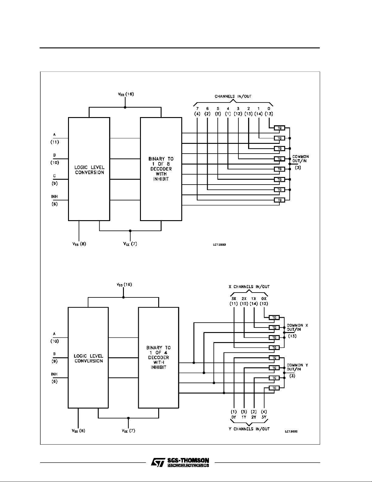
A built-in level shifting isincluded to allowthem an
inputrange ofupto± 6V(peak) foran analog signal
with digital control signalof 0 to 6V.
VEEsupplypin is provided for analog input signals.
They have aninhibit (INH) input terminal to disable
allthe switcheswhen high. Foroperation as adigital
multiplexer/demultiplexer, VEEis connected to
GND.
F1R
(CeramicPackage)
C1R
(Chip Carrier)
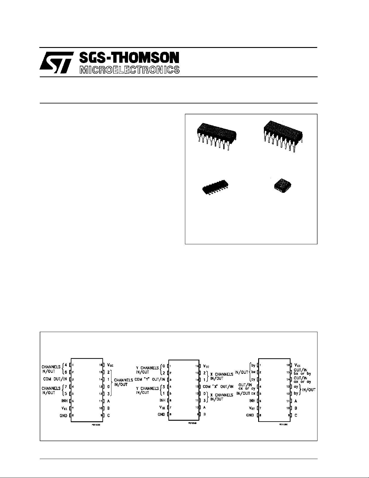
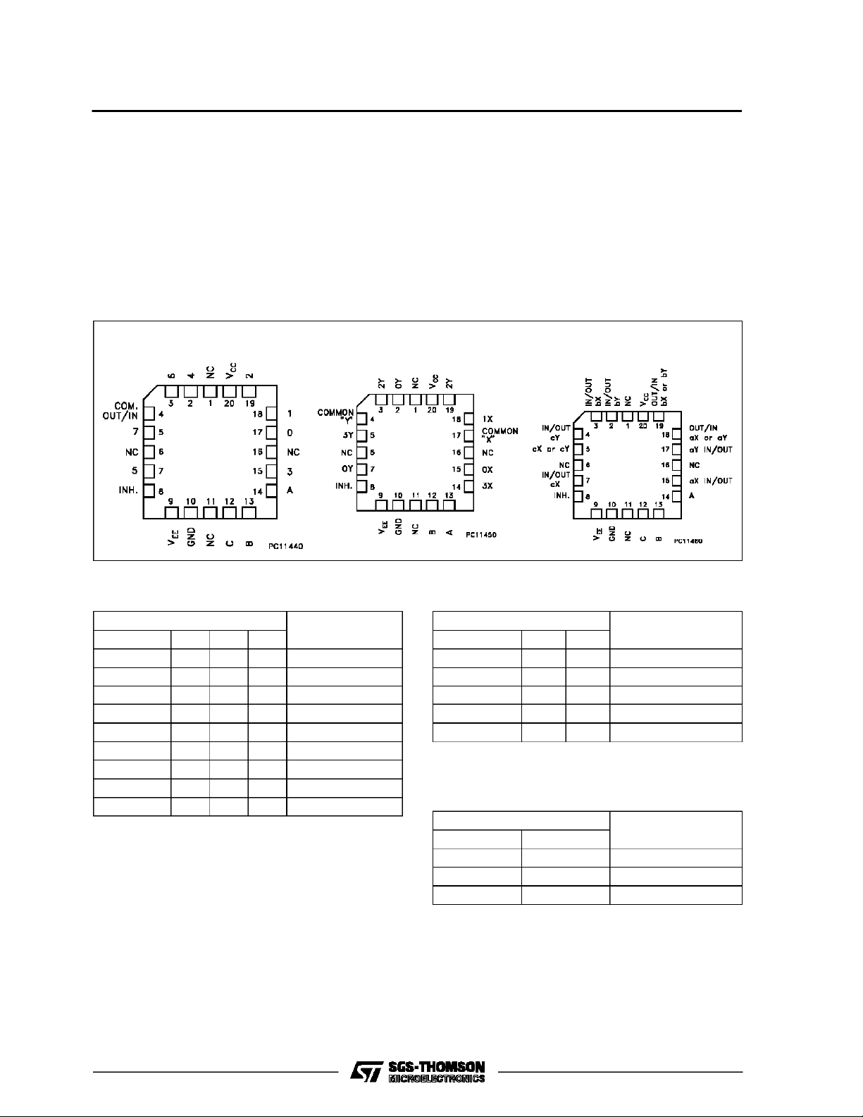
PIN CONNECTION (top view)
October 1993
HC4053HC4052HC4 051
1/15
M54/M74HC4051/4052/4053
DESCRIPTION
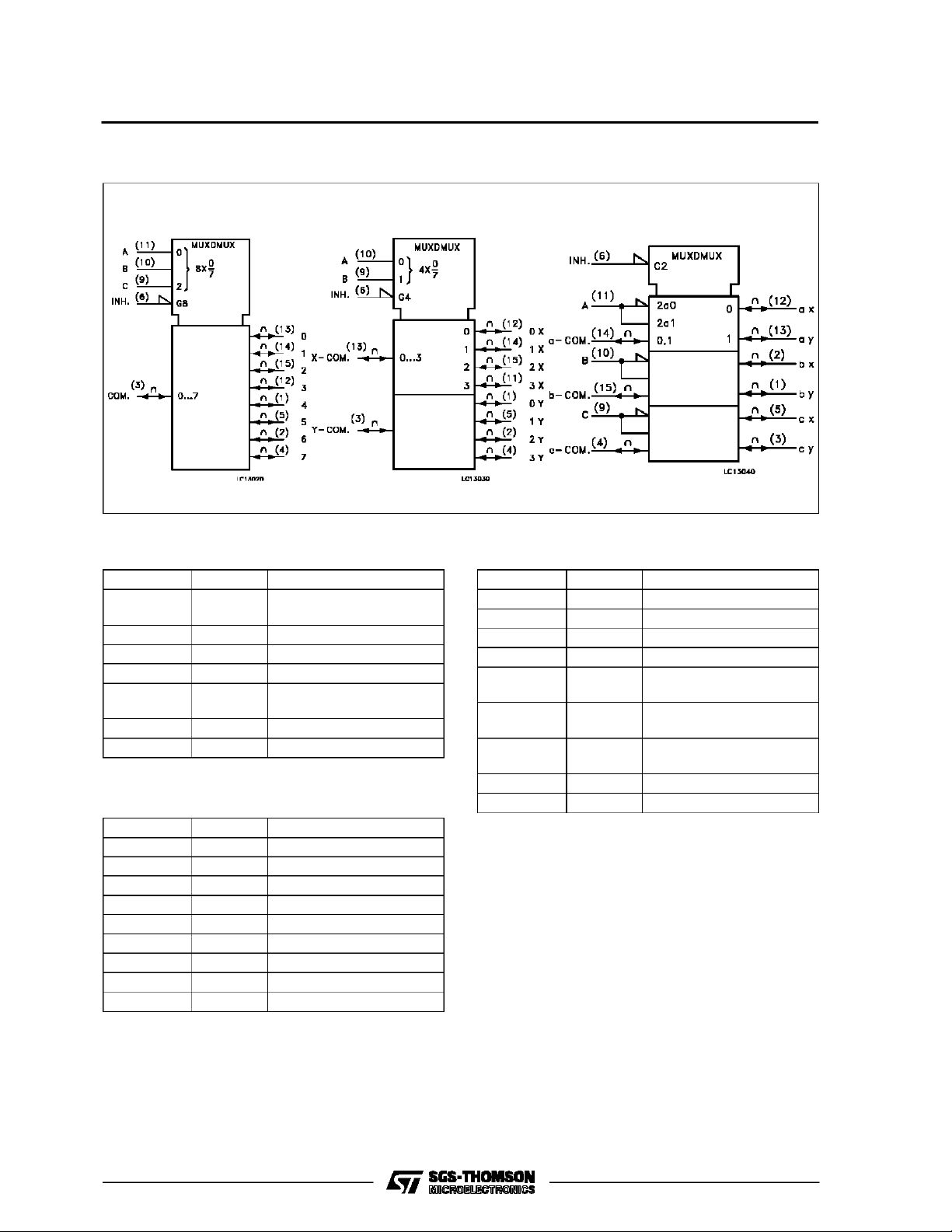
The HC4051 is a single 8 channel multiplexer
demultiplexer having threebinary control inputs A,
B and C to select 1 of 8 to be turned on, and
connected to the output.
The HC4052 has a pair of four channelmultiplexer
demultiplexer havingtwo controlinputsA and Bthat
CHIP CARRIER
selectone offour channels of the two sections.
The HC4053 is a triple two channel multiplexer
demultiplexer havingthree separate digitalcontrol
inputs A,B and C toselect independently one of a
pairof channles.
HC4053HC405 2HC4051
TRUTH TABLE (HC4051)
INPUT STATES
INHIBIT C B A
LLLL 0
LLLH 1
LLHL 2
LLHH 3
LHLL 4
LHLH 5
LHHL 6
LHHH 7
H X X X NONE
X: DON’TCARE
”ON” CHANNEL
TRUTH TABLE (HC 4052)
INPUT STATES
INHIBIT B A
L L L 0X, 0Y
L L H 1X, 1Y
L H L 2X, 2Y
L H H 3X, 3Y
H X X NONE
X: DON’T CARE
TRUTH TABLE (HC 4053)
INPUT STATES
INHIBIT A or B or C
L L ax or bx or cx
L H ay or by or cy
H X NONE
X: DON’T CARE
”ON” CHANNELS
”ON” CHANNELS
2/15
IEC LOGIC SYMBOLS
M54/M74HC4051/4052/4053
HC405 3HC4052HC4051
PIN DESCRIPTION (H C4051)
PIN No SYMBOL NAME AND FUNCTION
3 COM
Common Output/input
OUT/IN
6 INH INHIBIT Input
7V
EE
Negative Supply Voltage
11, 10, 9 A, B, C Select Inputs
13, 14, 15,
0 TO 7 Independent Input/Outputs
12, 1, 5, 2, 4
8 GND Ground (0V)
16 V
CC
Positive Supply Voltage
PIN DESCRIPTION (H C4053)
PIN No SYMBOL NAME AND FUNCTION
2, 1 bx, by Independent Input/Outputs
5, 3 cx, cy IndependentInput/Outputs
6 INH INHIBIT Input
7V
EE
11, 10, 9 A, B, C Select Inputs
12, 13 ax, ay Independent Input/Outputs
14, 15, 4 ax TO cy Common Output/input
8 GND Ground (0V)
16 V
CC
Negative Supply Voltage
Positive Supply Voltage
PIN DESCRIPTI ON (HC 4052)
PIN No SYMBOL NAME AND FUNCTION
1, 5, 2, 4 0Y TO 3Y Independent Input/Outputs
6 INH INHIBIT Input
7V
EE
10, 9 A, B Select Inputs
12, 14, 15,110X TO 3X Independent Input/Outputs
3 COM Y
OUT/IN
13 COM X
OUT/IN
8 GND Ground (0V)
16 V
CC
Negative Supply Voltage
Common X Output/input
Common Y Output/input
Positive Supply Voltage
3/15
M54/M74HC4051/4052/4053
FUNCTIONAL DIAGRAM
HC4051
HC4052
4/15
FUNCTIONAL DIAGRAM
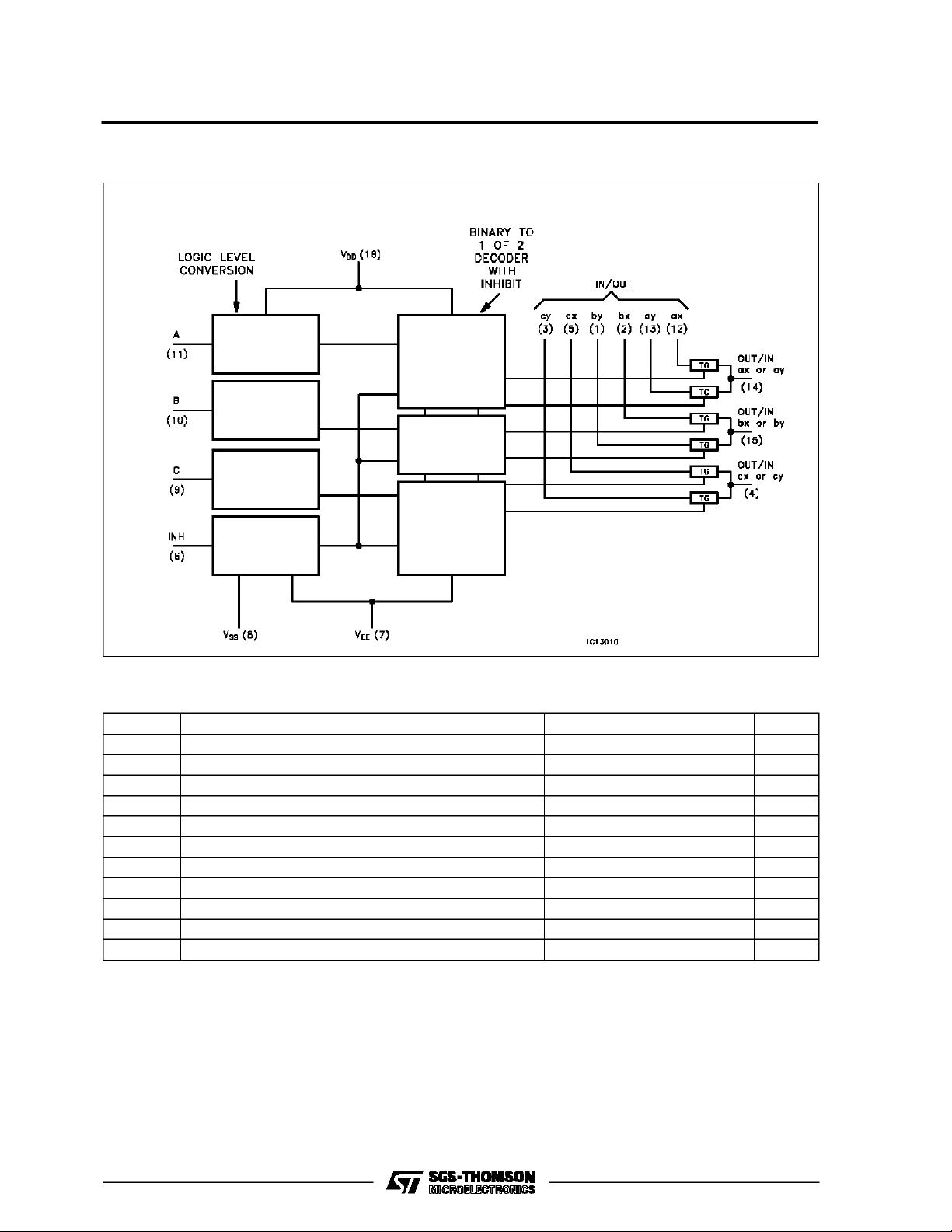
HC4053
M54/M74HC4051/4052/4053
ABSOLU TE M AXI MUM RATING S
Symbol Parameter Value Unit
V
CC
V
CC-VEE
V
IN
V
I/O
I
CK
I
IOK
I
T
I
CC
P
T
stg
T
AbsoluteMaximumRatingsarethosevalues beyond whichdamagetothedevicemayoccur. Functionaloperation undertheseconditionsis not implied.
(*)500 mW: ≅ 65oC derateto300 mWby 10mW/oC: 65oCto85oC
Supply Voltage Range -0.5 to +7 V
Supply Voltage Range -0.5 to 13 V
Control Input Voltage -0.5 to VCC+ 0.5 V
Switch I/O Voltage VEE- 0.5 to VCC+ 0.5 V
Control Input Diode Current ± 20 mA
I/O Diode Current ± 20 mA
Switch Through Current ± 25 mA
DC VCCor Ground Current ± 50 mA
Power Dissipation 500 (*) mW
D
Storage Temperature -65 to +150
Lead Temperature (10 sec) 300
L
o
C
o
C
5/15
 Loading...