

.HIGH SPEED
f
= 57 MHz(TYP.) at VCC=5V
MAX
.LOWPOWERDISSIPATION
ICC4 µA(MAX.) at TA=25°C
.HIGH NOISEIMMUNITY
V
NIH=VNIL
=28%VCC(MIN.)
.OUTPUT DRIVE CAPABILITY
10 LSTTL LOADS
.SYMMETRICALOUTPUT IMPEDANCE
|IOH|=IOL=4 mA(MIN.)
.BALANCEDPROPAGATION DELAYS
t
PLH=tPHL
.WIDE OPERATINGVOLTAGE RANGE
VCC(OPR)= 2V to 6 V
.PIN ANDFUNCTION COMPATIBLE
WITH 4022B
M54HC4022
M74HC4022
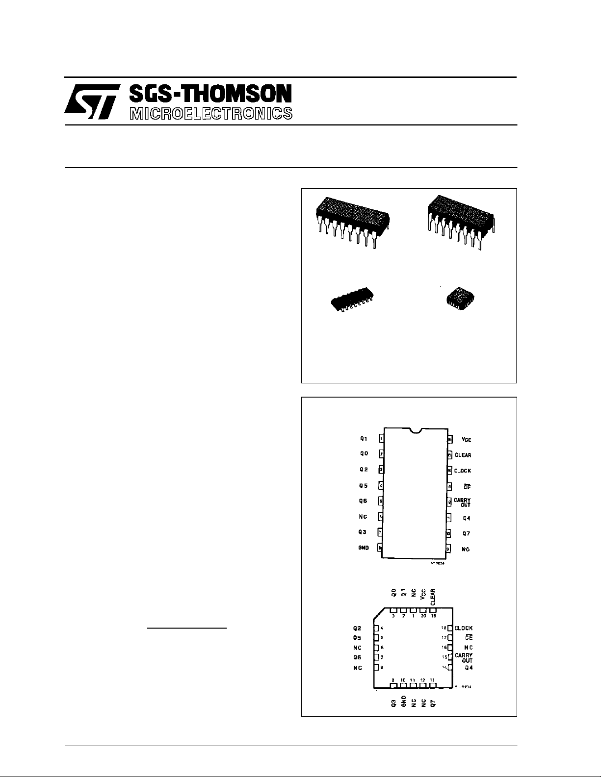
OCTAL COUNTER/DIVIDER
B1R
(PlasticPackage)
M1R
(MicroPackage)
ORDER CODES :
M54HC 4022F1R M74H C4022M1R
M74HC 4022B1R M74HC4 022C1R
F1R
(CeramicPackage)
C1R
(Chip Carrier)
DESCRIPTION
The M54/74HC4022 isa highspeedCMOSOCTAL
COUNTER/DIVIDER fabricated in silicon gate
C2MOS technology.
It has the same high speed performance of LSTTL
combined withtrue CMOSlowpower consumption.
It contains a 4-stage divide-by-8 Johnson counter
with8 decodedoutputs(Q0-Q7)andaCarry-outbit.
Thiscounterisadvanced onthepositive edge ofthe
clock signal when CLOCK ENABLE input is held
low, or is advanced on the negative edge of clock
enable signalwhen CLOCKinput is held high, and
the selectedoneof eightoutputsgoes high.Holding
the CLEAR inputhigh clearsthe counter to zeroregardless of the other input conditions. All inputsare
equipped with protection circuits against static discharge andtransientexcess voltage.
PIN CONNECTIONS(top view)
NC =
No Internal
Connection
October 1992
1/12
M54/M74HC4022
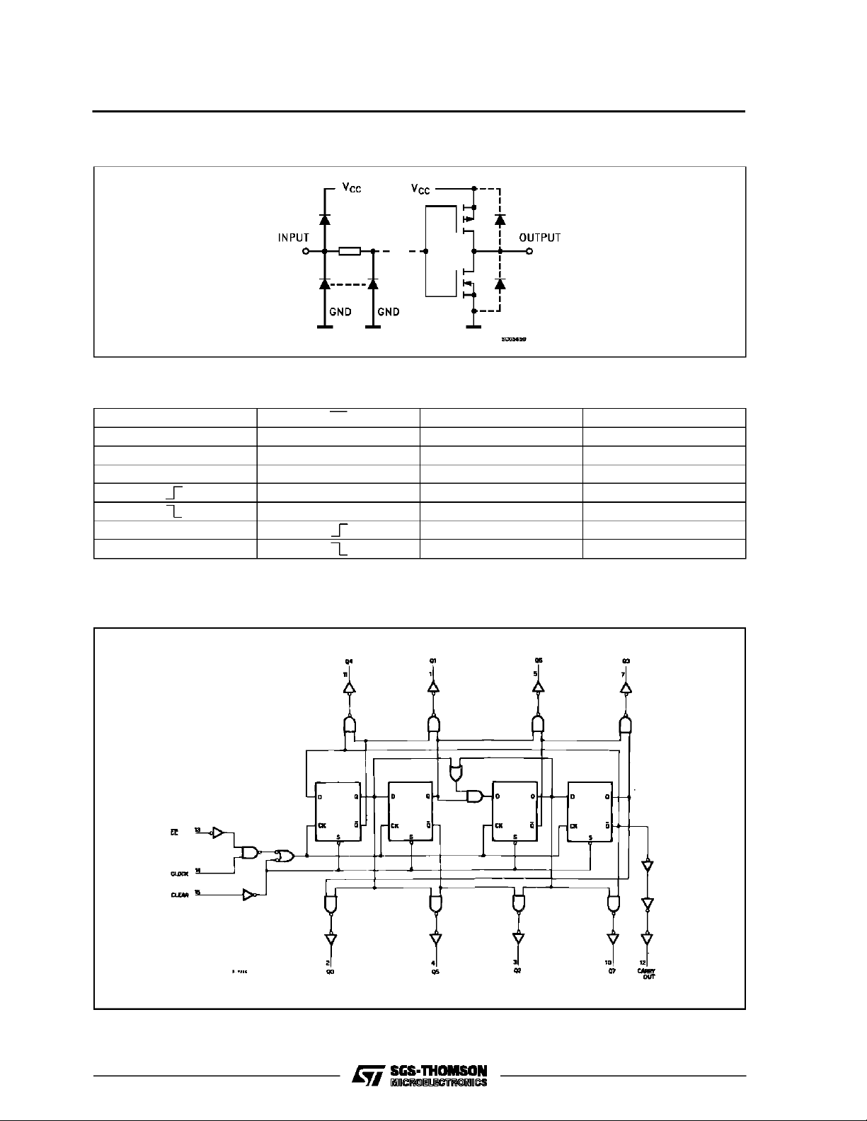
INPUT AND OUTPUT EQUIVALENT CIRCUIT
TRUTH TABLE
CLOCK CE CLEAR DECODER OUTPUT (H)
XXHQ0
L X L NO CHANGE
X H L NO CHANGE
L L NO CHANGE + 1
L L NO CHANGE
H L NO CHANGE
H L NO CHANGE + 1
X:DON’T CARE
LOGIC DIAGRAM
2/12
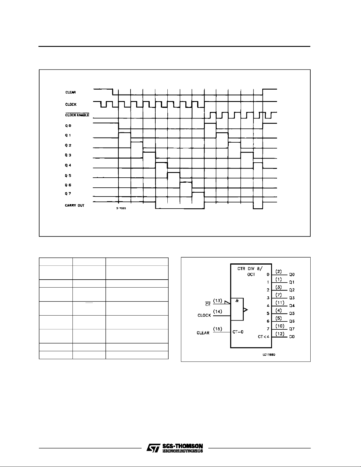
TIMING CHART
M54/M74HC4022
PIN DESCRIPTION
PIN No SYMBOL NAME AND FUNCTION
3, 2, 4, 7,
10, 1, 5, 11
6, 9 NC Not Connected
12 CARRY
13 CE Clock Input (HIGH to
14 CLOCK Clock Input (LOW to
15 CLEAR Master reset Input
8 GND Ground (0V)
16 V
Q0 to Q7 Decoded Outputs
Carry Output (Active
OUT
CC
LOW)
LOW, Edge-triggered)
HIGH, Edge-triggered)
(Active HIGH)
Positive Supply Voltage
IEC LOGIC SYMBOL
3/12
M54/M74HC4022
ABSOLU TE MAXIMU M RAT INGS
Symbol Parameter Value Unit
V
CC
V
V
O
I
IK
I
OK
I
O
I
or I
CC
P
D
T
stg
T
AbsoluteMaximumRatingsarethosevaluesbeyondwhichdamagetothedevicemayoccur.Functionaloperationunder theseconditionisnotimplied.
(*)500 mW: ≅ 65oC derateto300 mWby 10mW/oC: 65oCto85oC
RECO MM ENDED OPERATI N G CONDI TIONS
Symbol Parameter Value Unit
V
CC
V
I
V
O
T
op
t
r,tf
Supply Voltage -0.5 to +7 V
DC Input Voltage -0.5 to VCC+ 0.5 V
I
DC Output Voltage -0.5 to VCC+ 0.5 V
DC Input Diode Current ± 20 mA
DC Output Diode Current ± 20 mA
DC Output Source Sink Current Per Output Pin ± 25 mA
DC VCCor Ground Current ± 50 mA
GND
Power Dissipation 500 (*) mW
Storage Temperature -65 to +150
Lead Temperature (10 sec) 300
L
Supply Voltage 2 to 6 V
Input Voltage 0 to V
Output Voltage 0 to V
Operating Temperature: M54HC Series
M74HC Series
CC
CC
-55 to +125
-40 to +85
Input Rise and Fall Time VCC= 2 V 0 to 1000 ns
V
= 4.5 V 0 to 500
CC
V
= 6 V 0 to 400
CC
o
C
o
C
V
V
o
C
o
C
4/12
 Loading...