

.HIGH SPEED
tPD= 21 ns (typ.) ATVCC=5V
.LOWPOWERDISSIPATION
ICC=4µA(MAX.) AT TA=25oC
.HIGH NOISEIMMUNITY
V
NIH=VNIL
=28%VCC(MIN.)
.OUTPUT DRIVE CAPABILITY
10 LSTTL LOADS
.SYMMETRICALOUTPUT IMPEDANCE
|IOH|=IOL=4 mA(MIN.)
.BALANCEDPROPAGATION DELAYS
t
PLH=tPHL
.WIDE OPERATINGVOLTAGE RANGE
VCC(OPR)= 2 V TO6 V
.PIN AND FUNCTION COMPATIBLEWITH
4017B
M54HC4017
M74HC4017
DECADE COUNTER/DIVIDER
B1R
(PlasticPackage)
M1R
(MicroPackage)
ORDER CODES :
M54HC 4017F1R M74H C4017M1R
M74HC 4017B1R M74HC4 017C1R
F1R
(CeramicPackage)
C1R
(Chip Carrier)
DESCRIPTION
The M54/74HC4017 is a high speed CMOS DECADE COUNTER/DIVIDER fabricated in silicon
gate C2MOS technology. It has the same high
speed performance of LSTTL combined with true
CMOS low powerconsumption.
The M54/74HC4017 is a 5-stage Johnson counter
with 10decoded outputs.Each of the decoded outputs is normally low and sequentially goeshigh on
the lowtohigh transitionoftheclockinput.Each output stays high for one clock period of the 10 clock
period cycle. The CARRY output goes low to high
afterOUTPUT10goeslow, and canbeusedinconjunction with the CLOCKENABLE to cascadeseveralstages.
The CLOCKENABLE input disables countingwhen
in the high state. A RESET input is also provided
whichwhen takenhigh setsall thedecodedoutputs
low.
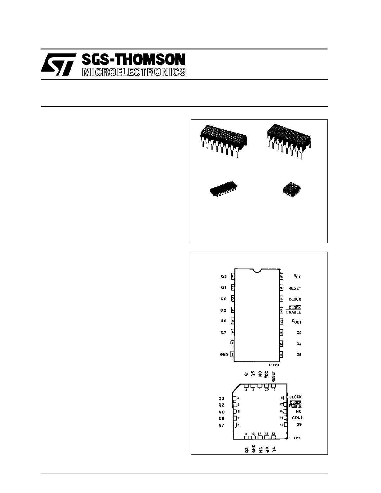
PIN CONNECTIONS(top view)
Q3
NC =
No Internal
Connection
October 1992
1/12
M54/M74HC4017
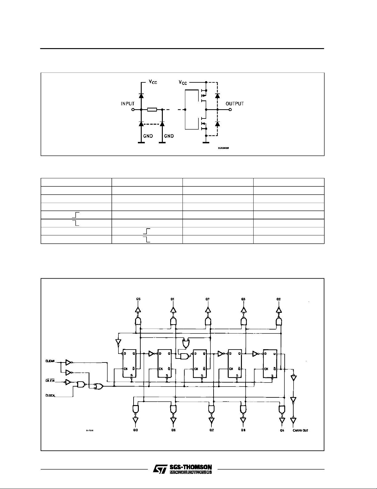
INPUT AND OUTPUT EQUIVALENT CIRCUIT
TRUTH TABLE
CLOCK CLOCK ENABLE CLEAR DECODE OUTPUT (H)
XXHQO
LXLQn
XHLQn
LLQn+1
LLQn
HLQn
HLQn+1
X:DON’TCARE
Qn: NO CHANGE
LOGIC DIAGRAM
2/12
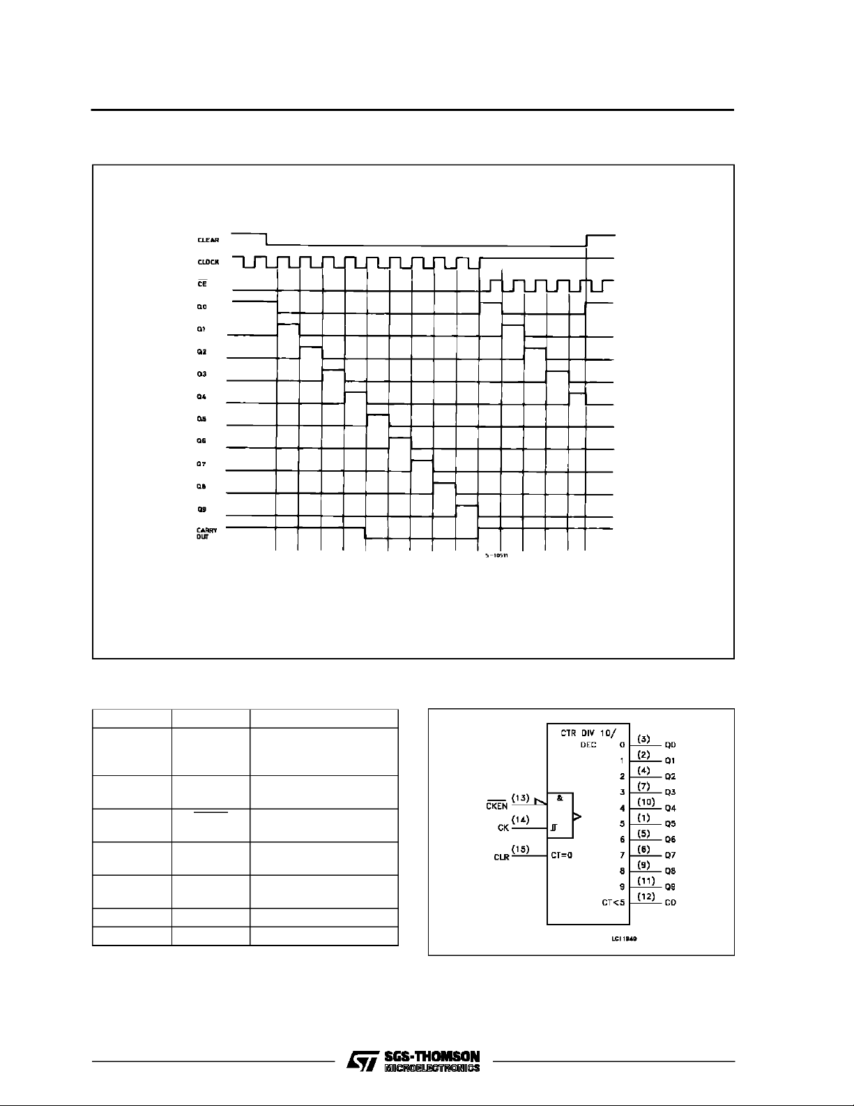
TIMING DIAGRAM
M54/M74HC4017
PIN DESCRIPTIO N
PIN No SYMBOL NAME AND FUNCTION
3, 2, 4, 7,
10, 1, 5, 6,
9, 11
12 C
13 CKEN Clock Enable Input
14 CLOCK Clock Input (LOW to
15 RESET Master Reset Input
8 GND Ground (0V)
16 V
Q0 to Q9 Decoded Outputs
OUT
CC
Carry Output (Active
LOW)
(Active LOW)
HIGH, Edge-triggered)
(Active HIGH)
Positive Supply Voltage
IEC LOGIC SYMBOL
3/12
M54/M74HC4017
ABSOLU TE MAXIMU M R AT INGS
Symbol Parameter Value Unit
V
CC
V
V
O
I
IK
I
OK
I
O
I
or I
CC
P
D
T
stg
T
AbsoluteMaximumRatingsarethose valuesbeyond whichdamage to thedevice mayoccur.Functional operation under these conditionisnotimplied.
(*)500 mW: ≅ 65oC derateto300 mWby 10mW/oC: 65oCto85oC
RECO MM ENDED O PERAT IN G CONDI TIONS
Symbol Parameter Value Unit
V
CC
V
I
V
O
T
op
t
r,tf
Supply Voltage -0.5 to +7 V
DC Input Voltage -0.5 to VCC+ 0.5 V
I
DC Output Voltage -0.5 to VCC+ 0.5 V
DC Input Diode Current ± 20 mA
DC Output Diode Current ± 20 mA
DC Output Source Sink Current Per Output Pin ± 25 mA
DC VCCor Ground Current ± 50 mA
GND
Power Dissipation 500 (*) mW
Storage Temperature -65 to +150
Lead Temperature (10 sec) 300
L
Supply Voltage 2 to 6 V
Input Voltage 0 to V
Output Voltage 0 to V
Operating Temperature: M54HC Series
M74HC Series
CC
CC
-55 to +125
-40 to +85
Input Rise and Fall Time VCC= 2 V 0 to 1000 ns
V
= 4.5 V 0 to 500
CC
V
= 6 V 0 to 400
CC
o
C
o
C
V
V
o
C
o
C
4/12
 Loading...