

.HIGH SPEED
tPD= 9 ns (TYP.)AT VCC=5V
.LOWPOWERDISSIPATION
ICC=1µA(MAX.) AT TA=25°C
.HIGH NOISEIMMUNITY
V
NIH=VNIL
=28%VCC(MIN.)
.LOW ”ON” RESISTANCE
RON=60Ω(TYP.)AT VCC= 9 V, I
=100 µA
I/O
.SINE WAVE DISTORSION
0.042 % (TYP.) AT VCC=9VPP, f = 1KHz
.WIDE OPERATINGVOLTAGE RANGE
VCC(OPR)= 2V TO 12 V
.PIN ANDFUNCTION COMPATIBLE
WITH 4016B
M54HC4016
M74HC4016
QUAD BILATERAL SWITCH
B1R
(PlasticPackage)
M1R
(MicroPackage)
ORDER CODES :
M54HC 4016F1R M74H C4016M1R
M74HC 4016B1R M74HC4 016C1R
F1R
(CeramicPackage)
C1R
(Chip Carrier)
DESCRIPTION
The M54/74HC4016 is a high speedCMOS QUAD
BILATERAL SWITCH fabricated in silicon gate
C2MOS technology. It has high speed performance
combined withtrue CMOSlowpower consumption.
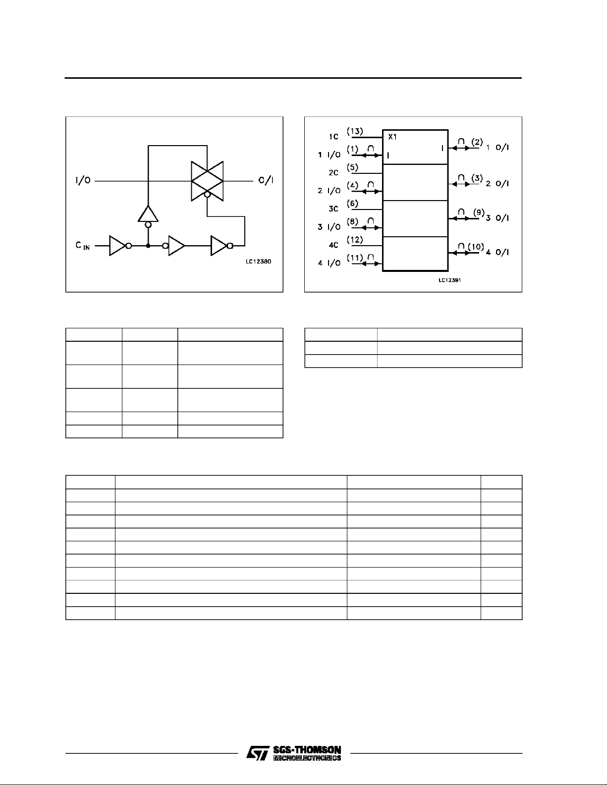
The C input is provided to control the switch ; the
switch is ON when the C input is held high and off
when Cis held low.
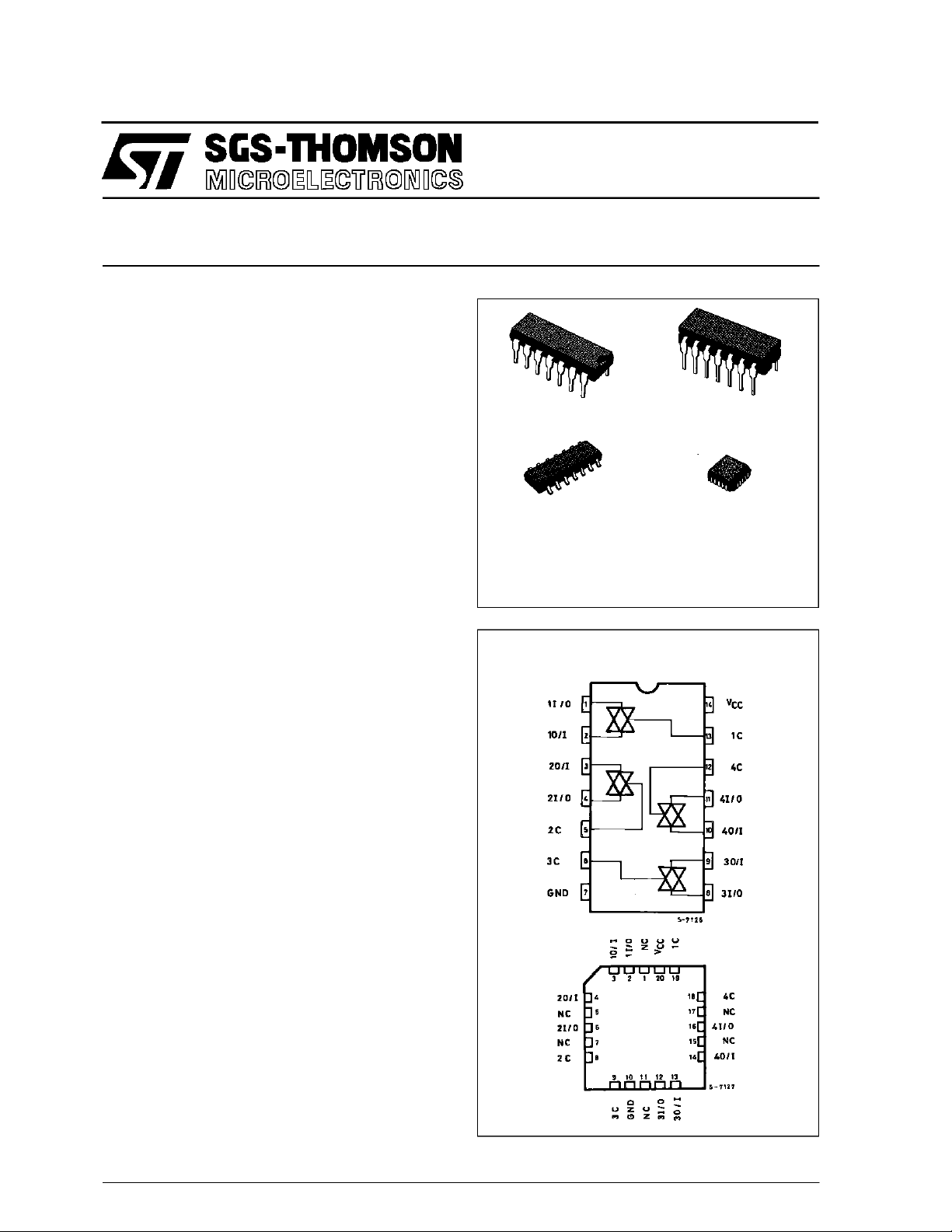
PIN CONNECTIONS(top view)
NC =
No Internal
Connection
October 1993
1/11
M54/M74HC4016
LOGIC DIAGRAM IEC LOGIC SYMBOL
PIN DESCRIPTION
PIN No SYMBOL NAME AND FUNCTION
1,4, 8, 11 1 to 4 I/O Independent
Inputs/Outputs
TRUTH TABLE
CONTROL SWITCH FUNCTION
HON
L OFF
2,3, 9, 10 1 to 4 O/I Independent
Outputs/Inputs
13,5, 6,12 1C to4C Enable Inputs (Active
HIGH)
7 GND Ground (0V)
14 V
CC
Positive Supply Voltage
ABSOLU TE MAXIMU M RAT ING
Symbol Parameter Value Unit
V
CC
V
IN
V
I/O
I
OK
I
I/OK
I
O
I
orI
CC
P
T
stg
T
AbsoluteMaximumRatingsarethose values beyond whichdamage tothedevicemayoccur. Functional operation under these conditionisnotimplied.
(*)500 mW: ≅ 65oC derateto300mWby 10mW/oC: 65oCto85oC
Supply Voltage -0.5 to+13 V
DC Input Voltage -0.5 toVCC+0.5 V
DC Input/Output Voltage -0.5 toVCC+0.5 V
Control Input DC Diode Current ± 20 mA
I/O DC Diode Current ± 20 mA
DC Output Source Sink Current Per Output Pin ± 25 mA
DC VCCor Ground Current ± 50 mA
GND
Power Dissipation 500(*) mW
D
Storage Temperature -65to +150
Lead Temperature (10 sec) 300
L
o
C
o
C
2/11
M54/M74HC4016
RECO MM ENDED OPERATI N G CONDI TIONS
Symbol Parameter Value Unit
V
V
V
T
t
r,tf
DC SPECIFICATIO NS
Symbol Parameter
V
IHC
V
ILC
R
ON
∆R
I
OFF
I
IZ
I
IN
I
CC
Supply Voltage 2 to 12 V
CC
Input Voltage (Control) 0 to V
I
Input/Output Voltage 0 to V
I/O
Operating Temperature: M54HC Series
op
M74HC Series
CC
CC
-55to +125
-40to +85
Input Rise and Fall Time VCC= 2 V 0 to1000 ns
V
= 4.5 V 0 to 500
CC
V
= 6 V 0 to 400
CC
V
= 10 V 0 to 250
CC
Test Conditions Value
T
High Level
Control Input
Voltage
=25oC
V
(V)
CC
A
54HC and 74HC
Min. Typ. Max. Min. Max. Min. Max.
2.0 1.5 1.5 1.5
4.5 3.15 3.15 3.15
9.0 6.3 6.3 6.3
-40 to 85oC
74HC
-55 to 125oC
12.0 8.4 8.4 8.4
Low Level
Control Input
Voltage
2.0 0.5 0.5 0.5
4.5 1.35 1.35 1.35
9.0 2.5 2.5 2.5
12.0 3.6 3.6 3.6
ON Resistance 4.5 VIN=V
9.0 85 170 213 260
12.0 60 120 150 180
4.5 V
9.0 60 120 150 200
12.0 50 100 125 150
Difference of ON
ON
Resistance
Between Switches
4.5
9.0 9
12.0 6
Input/Output
Leakage Current
12.0
(SWITCH OFF)
Switch Input
Leakage Current
(SWITCH ON,
12.0
=100µA
I/O
IN=VIHC
=100µA
I/O
V
IN=VIHC
≤ 100 µA
I/O
IHC
toGND
orGND
orGND
V
I/O=VCC
I
V
I/O=VCC
I
V
I/O=VCC
I
VOS=VCCorGND
VIS=VCCorGND
VIN=V
ILC
VOS=VCCorGND
VIN=V
IHC
160 320 400 450
80 160 200 250
16
±0.1 ±1 ±2 µA
±0.1 ±1 ±2 µA
OUTPUT OPEN)
Control Input
Current
Quiescent Supply
Current
VIN=VCCorGND ±0.1 ±1 ±1 µA
6.0
6.0 VIN=VCCorGND 1 10 20 µA
9.0 4 40 80
12.0 8 80 160
54HC
V
V
o
C
o
C
Unit
V
V
Ω
Ω
3/11
M54/M74HC4016
AC ELECTRICAL CHARACTERISTICS (CL=50pF,Inputtr=tf=6ns)
Test Conditions Value
T
=25oC
Symbol Parameter
ø
Phase Difference
I/O
Between Input
and Output
V
CC
(V)
2.0 20506575
4.5 5 10 13 15
9.0 4 8 10 12
A
54HC and 74HC
Min. Typ. Max. Min. Max. Min. Max.
12.0 3 7 9 11
t
t
PZL
PZH
Output Enable
Time
2.0 RL=1KΩ 40 100 125 150
4.5 10202530
9.0 8 15 20 24
12.0 7141821
t
PLZ
t
PHZ
Output Disable
Time
2.0 RL=1KΩ 60 150 190 225
4.5 15303845
9.0 10263336
12.0 8243032
C
C
C
C
PD
Input Capacitance 5 10 10 10 pF
IN
Switch Terminal
I/O
Capacitance
Feed Through
IOS
Capacitance
(*) Power Dissipation
9.0
9.0
5.0 15
5
1
Capacitance
(*) CPDisdefined as the value ofthe IC’sinternal equivalent capacitance whichis calculated fromthe operatingcurrentconsumption without load.
(Referto Test Circuit). Average operting current canbe obtained by the followingequation. ICC(opr) = CPD•VCC•fIN+I
-40 to 85oC
74HC
-55 to 125oC
54HC
CC
Unit
ns
ns
ns
pF
pF
pF
ANALO G SWITC H CHAR ACTE R ISTI CS (GND = 0 V TA=25oC)
Test Conditions Value
Symbol Parameter
Sine Wave Distortion (THD) 4.5 4.5 f
f
MAX
Frequency Response
(Switch ON)
Feedthrough Attenuation
(Switch OFF)
Crosstalk (Control Input to
Signal Output)
Crosstalk (Between Any
Switches)
V
VIN
CC
(V)
(Vp-p)
= 1 KHz RL=10KΩ CL= 50 pF 0.118
IN
9.0 9.0 0.042
12.0 12.0 0.032
4.5 Adjust fINvoltage to Obtain 0 dBm at VOS.
9.0 38
12.0 42
4.5 V
9.0 -50
Increase fINFrequency until dB Meter reads -3dB
RL=50Ω CL=50pF
iscentered atVCC/2. Adjust inputfor 0 dBm
IN
RL=600 Ω CL=50pF fIN=1 MHz sine wave
12.0 -50
4.5 R
9.0 23
=600Ω CL=50pF
L
fIN=1 MHz squarewave (tr=tf=6ns)
12.0 40
4.5 Adjust V
R
=600 Ω CL=50pF fIN=1 MHz sine wave
9.0 -50
L
toObtain 0 dBm at input
IN
12.0 -50
Typ.
23
-50
8
-50
Unit
%
MHz
dB
mV
dB
4/11
 Loading...