

.HIGH SPEED
f
= 84 MHz (TYP.) AT VCC=5V
MAX
.LOWPOWER DISSIPATION
ICC=4µA(MAX.) AT TA=25°C
.HIGH NOISE IMMUNITY
V
NIH=VNIL
=28%VCC(MIN.)
.OUTPUT DRIVE CAPABILITY
10 LSTTL LOADS
.SYMMETRICALOUTPUT IMPEDANCE
|IOH|=IOL=4 mA (MIN.)
.BALANCEDPROPAGATION DELAYS
t
PLH=tPHL
.WIDE OPERATING VOLTAGERANGE
VCC(OPR)= 2 V TO 6 V
.PIN AND FUNCTION COMPATIBLE WITH
54/74LS390
M54HC390
M74HC390
DUAL DECADE COUNTER
B1R
(PlasticPackage)
M1R
(MicroPackage)
ORDER CODES :
M54HC 390F1R M74H C390M1R
M74HC 390B1R M74HC3 90C1R
F1R
(CeramicPackage)
C1R
(Chip Carrier)
DESCRIPTION
The M54/74HC390 is a high speed CMOS DUAL
DECADE COUNTER fabricated in silicon gate
C2MOStechnology.It hasthesamehighspeedperformance of LSTTL combined with true CMOS low
powerconsumption.
Thisdualdecade counter containstwo independent
ripple carry counters. Each counter is composed of
a divide-by-two and divide-by-five counter. The
divide-by-two and divide-by-five counters can be
cascaded to form dual decade, dual biquinary, or
various combinations up to a single divide-by-100
counter.
Each4-bit counter is incremented onthe hightolow
transition (negative edge) of the clock input, and
eachhas an independent clear input. When clearis
set low all four bits of each counter are set to low.
This enables count truncation and allows the implementation of divide-by-N counterconfigurations.
All inputs are equipped with protection circuits
against static discharge and transient excess voltage.
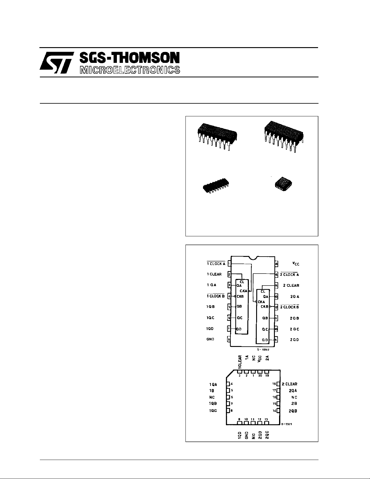
NC =
No InternalCon-
PIN CONNECTIONS (top view)
February 1993
1/13
M54/M74HC390
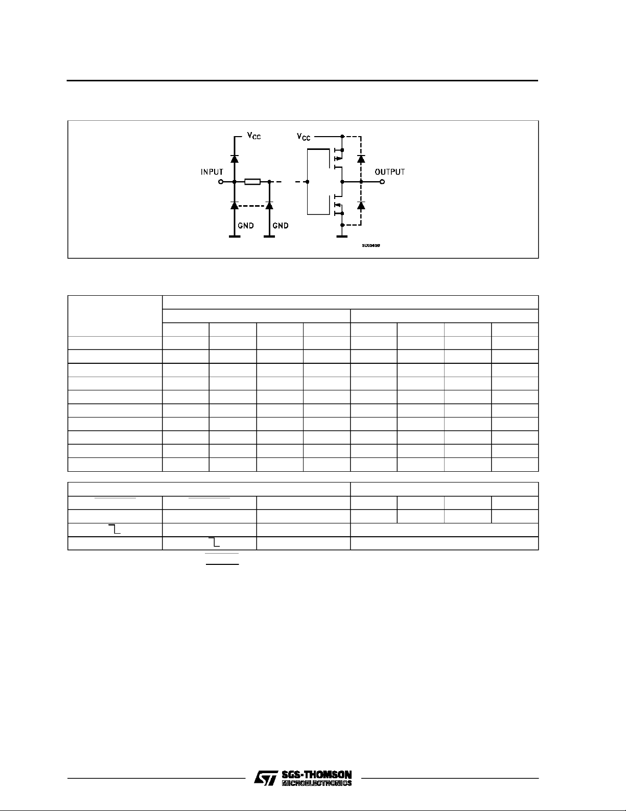
INPUT AND OUTPUT EQUIVALENT CIRCUIT
TRUTH TABLE
COUNT
QD QC QB QA QA QD QC QB
0 LLLLLLLL
1 LLLHLLLH
2LLHLLLHL
3LLHHLLHH
4 LHLLLHLL
5LHLHHLLL
6LHHLHLLH
7 LHHHHLHL
8 HLLLHLHH
9 HLLHHHLL
BCD COUNT * BI-QUINARY **
OUTPUTS
INPUTS OUTPUTS
CLOCK A CLOCK B CLEAR QA QB QC QD
X X H LLLL
X L BINARY COUNT UP
X L QUINARY COUNT UP
Note: * Output QA is connected toinput CLOCK Bfor BCD count.
** OutputQD isconnected to inputCLOCKA forbi-quinary count.
2/13
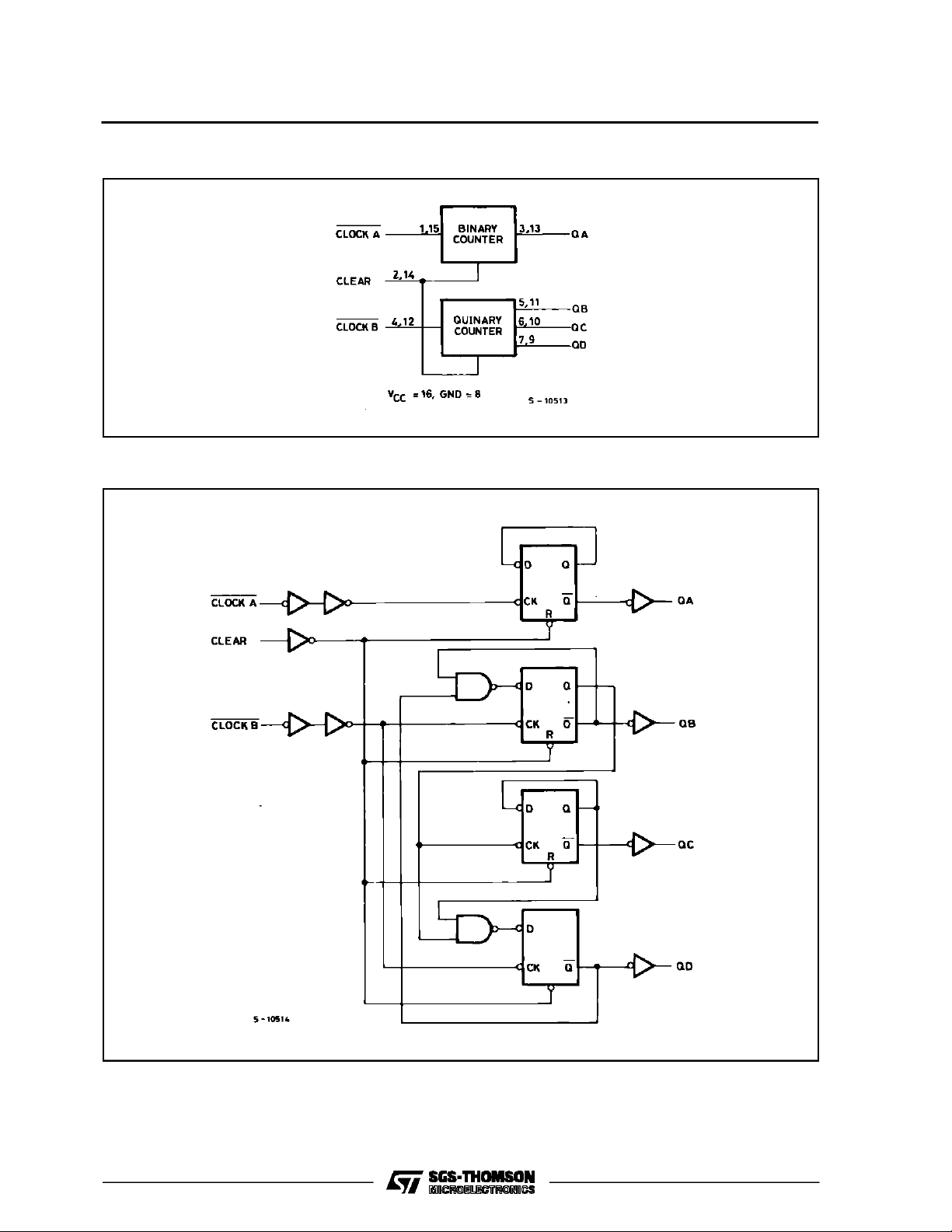
BLOCK DIAGRAM
LOGIC DIAGRAM
M54/M74HC390
3/13
M54/M74HC390
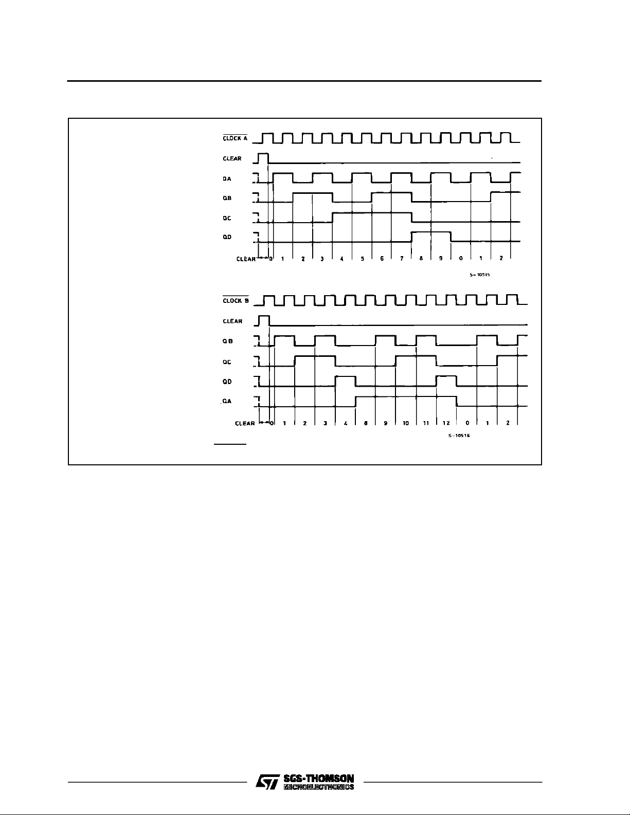
TIMING CHART
(1) BCDCOUNT SEQUENCE *
(2) BI-QUINARYCOUNT SEQUENCE**
*OUTPUTQA IS CONNECTEDTO INPUTCLOCK B
4/13

M54/M74HC390
PIN DESCRIPTION
IEC LOGIC SYMBOL
PIN No SYMBOL NAME AND FUNCTION
1, 15 1 CLOCK A
2 CLOCK B
Clock Input Divide by 2
Section (HIGH to LOW
Edge-triggered)
2, 14 1 CLEAR
2 CLEAR
Asynchronous Master
Reset Inputs
3, 5, 6, 7 1QA to 1QD Flip Flop Outputs
4, 12 1 CLOCK B
2 CLOCK B
Clock Input Divide by 5
Section (HIGH to LOW
Edge-triggered)
13, 11, 10, 9 2QA to 2QD Flip Flop Outputs
8 GND Ground (0V)
16 V
CC
Positive Supply Voltage
ABSOLU TE M AXIMU M R AT INGS
Symbol Parameter Value Unit
V
CC
V
V
O
I
IK
I
OK
I
O
or I
I
CC
P
T
stg
T
AbsoluteMaximumRatingsarethose values beyondwhichdamagetothedevice mayoccur.Functionaloperationunder theseconditionisnotimplied.
(*)500 mW:≅ 65oC derateto 300 mWby 10mW/oC: 65oCto85oC
Supply Voltage -0.5 to +7 V
DC Input Voltage -0.5 to VCC+ 0.5 V
I
DC Output Voltage -0.5 to VCC+ 0.5 V
DC Input Diode Current ± 20 mA
DC Output Diode Current ± 20 mA
DC Output Source Sink Current Per Output Pin ± 25 mA
DC VCCor Ground Current ± 50 mA
GND
Power Dissipation 500 (*) mW
D
Storage Temperature -65 to +150
Lead Temperature (10 sec) 300
L
o
C
o
C
RECO MM ENDED OPERATI N G C ONDI TIONS
Symbol Parameter Value Unit
V
T
t
V
V
r,tf
Supply Voltage 2 to 6 V
CC
Input Voltage 0 to V
I
Output Voltage 0 to V
O
Operating Temperature: M54HC Series
op
M74HC Series
CC
CC
-55 to +125
-40 to +85
Input Rise and Fall Time VCC= 2 V 0 to 1000 ns
V
= 4.5 V 0 to 500
CC
= 6 V 0 to 400
V
CC
V
V
o
C
o
C
5/13

M54/M74HC390
DC SPECIFICATIONS
Symbol Parameter
V
V
V
V
I
High Level Input
IH
Voltage
Low Level Input
IL
Voltage
High Level
OH
Output Voltage
Low Level Output
OL
Voltage
I
Input Leakage
I
Current
Quiescent Supply
CC
Current
Test Conditions Value
V
(V)
CC
=25oC
A
54HC and 74HC
Min. Typ. Max. Min. Max. Min. Max.
-40 to 85oC
74HC
-55 to 125oC
54HC
Unit
T
2.0 1.5 1.5 1.5
4.5 3.15 3.15 3.15
6.0 4.2 4.2 4.2
2.0 0.5 0.5 0.5
4.5 1.35 1.35 1.35
6.0 1.8 1.8 1.8
2.0
4.5 4.4 4.5 4.4 4.4
6.0 5.9 6.0 5.9 5.9
4.5 I
6.0 I
2.0
4.5 0.0 0.1 0.1 0.1
6.0 0.0 0.1 0.1 0.1
4.5 I
6.0 I
6.0
=
V
I
IO=-20 µA
V
IH
or
V
IL
=-4.0 mA 4.18 4.31 4.13 4.10
O
=-5.2 mA 5.68 5.8 5.63 5.60
O
V
=
I
IO=20µA
V
IH
or
V
IL
= 4.0 mA 0.17 0.26 0.33 0.40
O
= 5.2 mA 0.18 0.26 0.33 0.40
O
VI=VCCor GND ±0.1 ±1 ±1 µA
1.9 2.0 1.9 1.9
0.0 0.1 0.1 0.1
6.0 VI=VCCor GND 4 40 80 µA
V
V
V
V
6/13

M54/M74HC390
AC ELECTRICAL CHARACTERISTICS (CL=50pF,Inputtr=tf=6ns)
Test Conditions Value
T
=25oC
Symbol Parameter
t
t
TLH
THL
Output Transition
Time
V
CC
(V)
2.0 30 75 95 110
4.5 8151922
A
54HC and 74HC
Min. Typ. Max. Min. Max. Min. Max.
6.0 7131619
t
PLH
t
PHL
Propagation
Delay Time
(CLOCK A - QA)
t
t
PLH
PHL
Propagation
Delay Time
(CLOCK A - QB, QD)
t
t
PLH
PHL
Propagation
Delay Time
(CLOCK A - QC)
t
t
PLH
PHL
Propagation
Delay Time
(CLOCK B - QC)
t
PHL
Propagation
Delay Time
(CLEAR - Qn
f
MAX
Maximum Clock
Frequency
(CLOCK A - QA)
f
MAX
Maximum Clock
Frequency
(CLOCK B - QB)
t
W(H)
t
W(L)
Minimum Pulse
Wisth
(CLOCK)
t
(W)H
Minimum Pulse
Wisth
(CLEAR)
t
REM
Propagation
Delay Time
2.0 42 120 150 180
4.5 14 24 30 36
6.0 12 20 26 31
2.0 45 120 150 180
4.5 15 24 30 36
6.0 13 20 26 31
2.0 QA Connected
4.5 36 56 70 84
to CKB
108 280 350 420
6.0 31 48 60 71
2.0 72 185 230 280
4.5 24 37 46 56
6.0 20 31 39 48
2.0 45 125 155 190
4.5 15 25 31 38
6.0 13 21 26 32
2.0 8.4 17 6.8 5.6
4.5 42 65 34 28
6.0 50 79 40 33
2.0 8.4 17 6.8 5.6
4.5 42 67 34 28
6.0 50 79 40 33
2.0 24 75 95 110
4.5 6151922
6.0 5131619
2.0 24 75 95 110
4.5 6151922
6.0 5131619
2.0 25 30 35
4.5 5 6 7
6.0 5 5 6
C
C
PD
Input Capacitance 5 10 10 10 pF
IN
(*) Power Dissipation
84
Capacitance
(*) CPDisdefined as the valueof the IC’s internal equivalent capacitance which is calculated fromthe operatingcurrent consumption without load.
(Referto Test Circuit).Average operting current can be obtained bythe followingequation. ICC(opr) = CPD•VCC•fIN+I
-40 to 85oC
74HC
-55 to 125oC
54HC
CC
Unit
ns
ns
ns
ns
ns
ns
ns
ns
ns
ns
ns
pF
7/13

M54/M74HC390
TEST CIRCUIT ICC(Opr.)
WHENTHE OUTPUTSDRIVECAPACITIVELOAD, TOTALCURRENT CONSUMPTIONIS TOBEA SUMOF THE VALUECALCULATED
FROMCPDAND∆ICCOBTAINEDFROM THEFOLLOWING FORMULA.
f
Ca
∆ICC=f
Ca – Cd ARE THECAPACITANCEAT QA ∼ QD OUTPUT.
.
V
CK
CC
CK
.
+
2
2
2
Cb
Cc
Cd
.
.
+
V
CC
5
+
5
5
SWITCHING CHARACTERISTICS TEST WAVEFORM
8/13

Plastic DIP16 (0.25) MECHANICAL DATA
M54/M74HC390
DIM.
MIN. TYP. MAX. MIN. TYP. MAX.
a1 0.51 0.020
B 0.77 1.65 0.030 0.065
b 0.5 0.020
b1 0.25 0.010
D 20 0.787
E 8.5 0.335
e 2.54 0.100
e3 17.78 0.700
F 7.1 0.280
I 5.1 0.201
L 3.3 0.130
Z 1.27 0.050
mm inch
P001C
9/13

M54/M74HC390
Ceramic DIP16/1 MECHANICAL DATA
DIM.
MIN. TYP. MAX. MIN. TYP. MAX.
A 20 0.787
B 7 0.276
D 3.3 0.130
E 0.38 0.015
e3 17.78 0.700
F 2.29 2.79 0.090 0.110
G 0.4 0.55 0.016 0.022
H 1.17 1.52 0.046 0.060
L 0.22 0.31 0.009 0.012
M 0.51 1.27 0.020 0.050
N 10.3 0.406
P 7.8 8.05 0.307 0.317
Q 5.08 0.200
mm inch
10/13
P053D

SO16 (Narrow) MECHANICAL DATA
M54/M74HC390
DIM.
MIN. TYP. MAX. MIN. TYP. MAX.
A 1.75 0.068
a1 0.1 0.2 0.004 0.007
a2 1.65 0.064
b 0.35 0.46 0.013 0.018
b1 0.19 0.25 0.007 0.010
C 0.5 0.019
c1 45° (typ.)
D 9.8 10 0.385 0.393
E 5.8 6.2 0.228 0.244
e 1.27 0.050
e3 8.89 0.350
F 3.8 4.0 0.149 0.157
G 4.6 5.3 0.181 0.208
L 0.5 1.27 0.019 0.050
M 0.62 0.024
S8°(max.)
mm inch
P013H
11/13

M54/M74HC390
PLCC20 MECHANICAL DATA
DIM.
MIN. TYP. MAX. MIN. TYP. MAX.
A 9.78 10.03 0.385 0.395
B 8.89 9.04 0.350 0.356
D 4.2 4.57 0.165 0.180
d1 2.54 0.100
d2 0.56 0.022
E 7.37 8.38 0.290 0.330
e 1.27 0.050
e3 5.08 0.200
F 0.38 0.015
G 0.101 0.004
M 1.27 0.050
M1 1.14 0.045
mm inch
12/13
P027A

M54/M74HC390
Information furnished is believed to be accurate and reliable. However, SGS-THOMSON Microelectronics assumes no responsability for the
consequences of use of such information nor for any infringement of patents or other rights of third parties which may results from its use. No
license is granted byimplication or otherwise under any patent or patentrights of SGS-THOMSON Microelectronics. Specificationsmentioned
in this publication are subject to change without notice. This publication supersedes and replaces all information previously supplied.
SGS-THOMSON Microelectronicsproducts are not authorized foruse ascritical componentsin life support devices or systems without express
written approval of SGS-THOMSON Microelectonics.
1994 SGS-THOMSON Microelectronics - All Rights Reserved
Australia - Brazil - France - Germany - Hong Kong - Italy - Japan - Korea - Malaysia - Malta - Morocco - The Netherlands -
Singapore -Spain - Sweden- Switzerland -Taiwan - Thailand - UnitedKingdom - U.S.A
SGS-THOMSON Microelectronics GROUP OF COMPANIES
13/13
 Loading...