

.HIGH SPEED
tPD= 14 ns(TYP.) AT VCC=5V
.LOWPOWER DISSIPATION
ICC=1µA(MAX.) AT TA=25°C
.HIGH NOISE IMMUNITY
V
NIH=VNIL
=28%VCC(MIN.)
.OUTPUT DRIVE CAPABILITY
10 LSTTL LOADS
.SYMMETRICALOUTPUT IMPEDANCE
|IOH|=IOL=4 mA (MIN.)
.BALANCEDPROPAGATION DELAYS
t
PLH=tPHL
.WIDE OPERATING VOLTAGERANGE
VCC(OPR)= 2 V TO 6 V
.PIN AND FUNCTION COMPATIBLE WITH
54/74LS375
M54HC375
M74HC375
QUAD D TYPE LATCH
B1R
(PlasticPackage)
M1R
(MicroPackage)
ORDER CODES :
M54HC 375F1R M74H C375M1R
M74HC 375B1R M74HC3 75C1R
F1R
(CeramicPackage)
C1R
(Chip Carrier)
DESCRIPTION
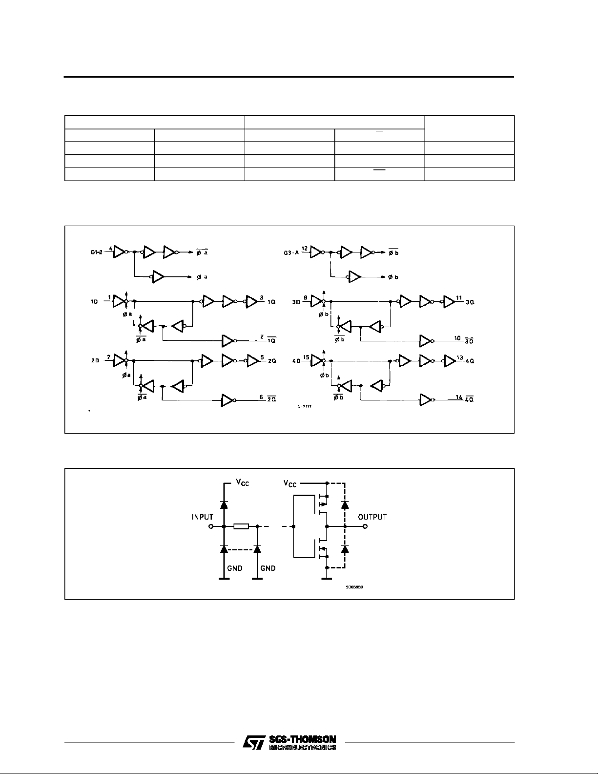
The M54/74HC375isahigh speedCMOSQUADD
TYPE LATCH fabricated in silicon gate C2MOS
technology. It has the same high speed performanceofLSTTL combinedwithtrue CMOSlowpower
consumption. It contains twogroupsof 2-bit latches
controlled by an enable input(G1.2orG3.4).
Thesetwolatchgroups can be usedinthe different
circuits.Each latch hasQ and Q outputs(1Q to 4Q
and 1Q to 4Q). The data applied to the data input is
transferred to theQ and Q outputs whenthe enable
input is taken high and the outputs will follow the
data input as long as the enable inputis kept high.
When the enable inputis takenlow, the information
data applied to thedata inputat that timeis retained
at the outputs.
All inputs are equipped with protection circuits
against static discharge and transient excess voltage.
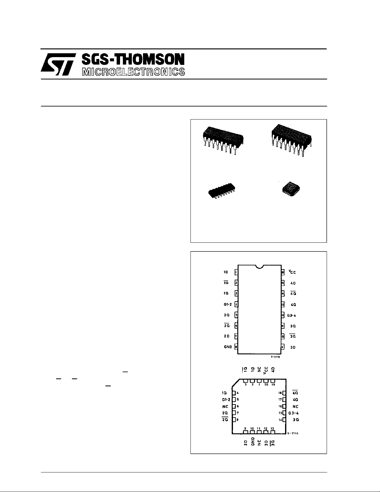
PIN CONNECTIONS (top view)
NC =
No Internal
Connection
February 1993
1/11
M54/M74HC375
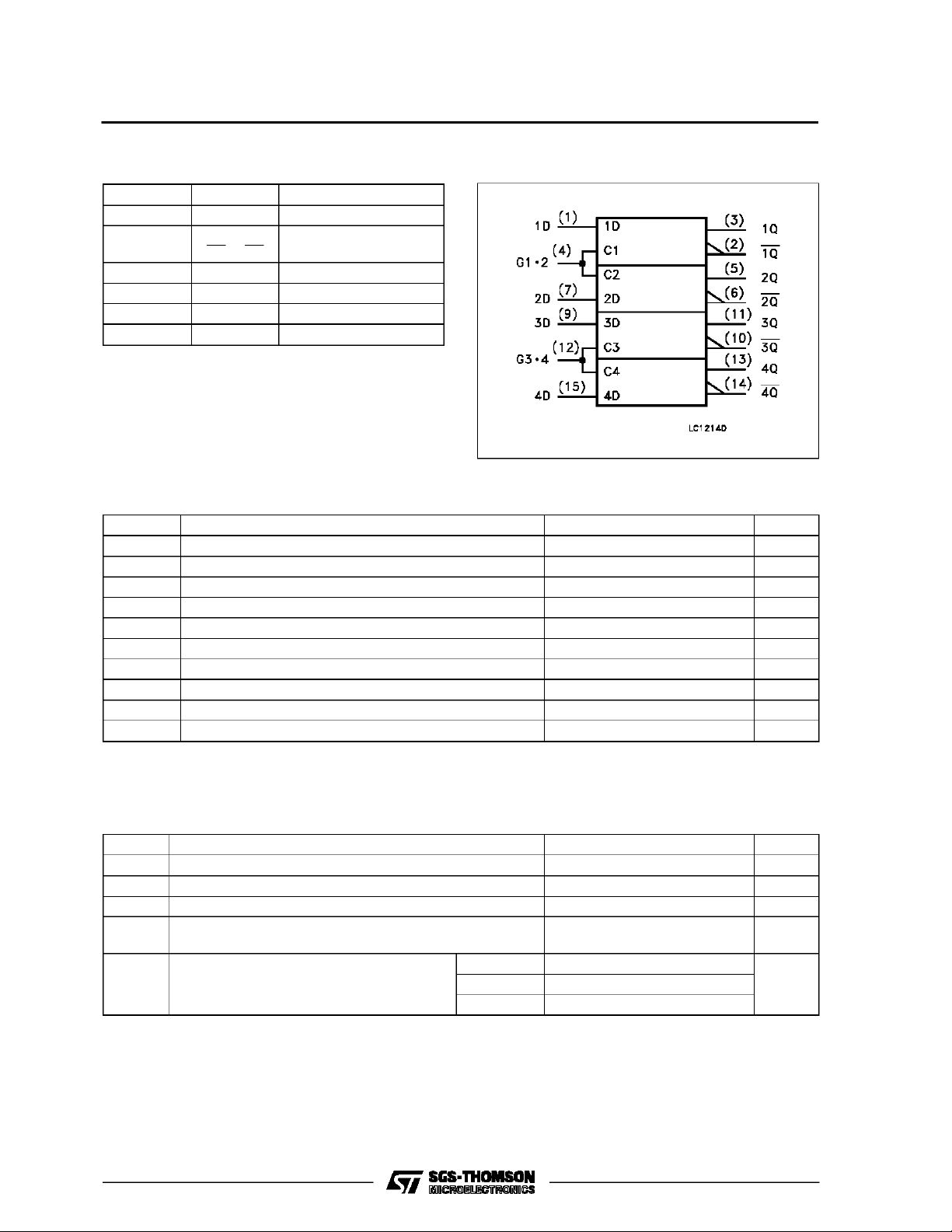
TRUTH TABLE
INPUTS OUTPUTS
DGQQ
LHLH
HHHL
X L Qn Qn LATCH
X:DON’T CARE
LOGIC DIAGRAM
FUNCTION
INPUT AND OUTPUT EQUIVALENT CIRCUIT
2/11
M54/M74HC375
PIN DESCRIPTION
IEC LOGIC SYMBOL
PIN No SYMBOL NAME AND FUNCTION
1, 7, 9, 15 1D to 4D Data Inputs
3, 5, 11, 13,
2, 6, 10, 14
1Q to 4Q
1Q to 4Q
Outputs
4 G1- 2 Enable Input
12 G3 - 4 Enable Input
8 GND Ground (0V)
16 V
CC
Positive Supply Voltage
ABSOLU TE M AXIMU M R AT INGS
Symbol Parameter Value Unit
V
CC
V
V
O
I
IK
I
OK
I
O
or I
I
CC
P
D
T
stg
T
AbsoluteMaximumRatingsarethose values beyondwhichdamagetothedevice mayoccur. Functionaloperationunder theseconditionisnotimplied.
(*)500 mW:≅ 65oC derateto 300 mWby 10mW/oC: 65oCto85oC
Supply Voltage -0.5 to +7 V
DC Input Voltage -0.5 to VCC+ 0.5 V
I
DC Output Voltage -0.5 to VCC+ 0.5 V
DC Input Diode Current ± 20 mA
DC Output Diode Current ± 20 mA
DC Output Source Sink Current Per Output Pin ± 25 mA
DC VCCor Ground Current ± 50 mA
GND
Power Dissipation 500 (*) mW
Storage Temperature -65 to +150
Lead Temperature (10 sec) 300
L
o
C
o
C
RECO MM ENDED OPERAT I N G C ONDI TIONS
Symbol Parameter Value Unit
V
T
t
V
V
r,tf
Supply Voltage 2 to 6 V
CC
Input Voltage 0 to V
I
Output Voltage 0 to V
O
Operating Temperature: M54HC Series
op
M74HC Series
CC
CC
-55 to +125
-40 to +85
Input Rise and Fall Time VCC= 2 V 0 to 1000 ns
V
= 4.5 V 0 to 500
CC
= 6 V 0 to 400
V
CC
V
V
o
C
o
C
3/11
M54/M74HC375
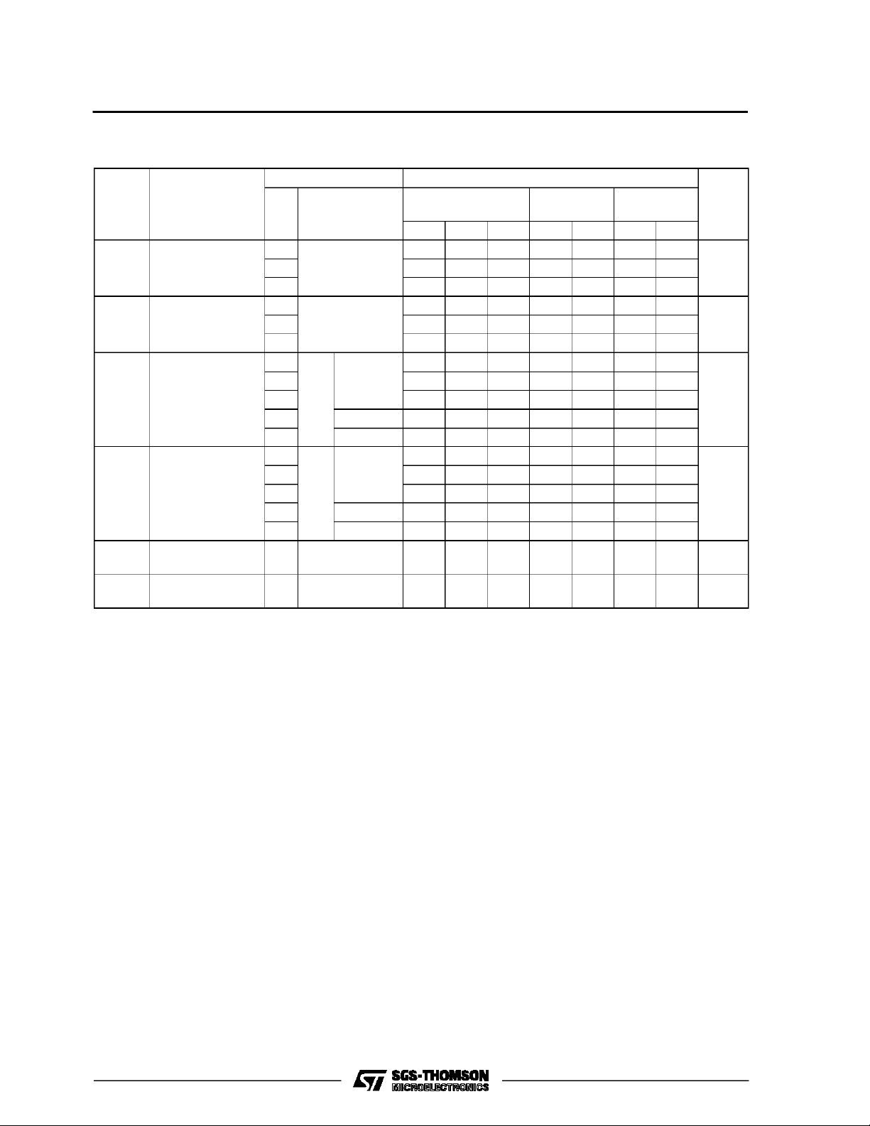
DC SPECIFICATIONS
Symbol Parameter
V
V
V
V
I
High Level Input
IH
Voltage
Low Level Input
IL
Voltage
High Level
OH
Output Voltage
Low Level Output
OL
Voltage
I
Input Leakage
I
Current
Quiescent Supply
CC
Current
Test Conditions Value
V
(V)
CC
=25oC
A
54HC and 74HC
Min. Typ. Max. Min. Max. Min. Max.
-40 to 85oC
74HC
-55 to 125oC
54HC
Unit
T
2.0 1.5 1.5 1.5
4.5 3.15 3.15 3.15
6.0 4.2 4.2 4.2
2.0 0.5 0.5 0.5
4.5 1.35 1.35 1.35
6.0 1.8 1.8 1.8
2.0
4.5 4.4 4.5 4.4 4.4
6.0 5.9 6.0 5.9 5.9
4.5 I
6.0 I
2.0
4.5 0.0 0.1 0.1 0.1
6.0 0.0 0.1 0.1 0.1
4.5 I
6.0 I
6.0
=
V
I
IO=-20 µA
V
IH
or
V
IL
=-4.0 mA 4.18 4.31 4.13 4.10
O
=-5.2 mA 5.68 5.8 5.63 5.60
O
V
=
I
IO=20µA
V
IH
or
V
IL
= 4.0 mA 0.17 0.26 0.33 0.40
O
= 5.2 mA 0.18 0.26 0.33 0.40
O
VI=VCCor GND ±0.1 ±1 ±1 µA
1.9 2.0 1.9 1.9
0.0 0.1 0.1 0.1
6.0 VI=VCCor GND 2 20 40 µA
V
V
V
V
4/11

M54/M74HC375
AC ELECTRICAL CHARACTERISTICS (CL=50pF,Inputtr=tf=6ns)
Test Conditions Value
T
=25oC
Symbol Parameter
t
t
TLH
THL
Output Transition
Time
V
CC
(V)
2.0 30 75 95 110
4.5 8151922
A
54HC and 74HC
Min. Typ. Max. Min. Max. Min. Max.
6.0 7131619
t
PLH
t
PHL
Propagation
Delay Time
(DATA - Q, Q)
t
t
PLH
PHL
Propagation
Delay Time
(G - Q, Q)
t
(W)H
Minimum Enable
Pulse Width
(G)
Minimum Set-up
t
s
Time
(DATA - G)
Minimum Hold
t
h
Time
(DATA - G)
C
C
PD
Input Capacitance 5 10 10 10 pF
IN
(*) Power Dissipation
2.0 56 115 145 175
4.5 14 23 29 35
6.0 12 20 25 30
2.0 52 105 130 160
4.5 13 21 26 32
6.0 11 18 22 27
2.0 12 75 95 115
4.5 3151923
6.0 3131620
2.0 20 75 95 115
4.5 5151923
6.0 4131620
2.0 0 0 0
4.5 0 0 0
6.0 0 0 0
52
Capacitance
(*) CPDisdefined as the valueof the IC’s internal equivalent capacitance which is calculated fromthe operatingcurrent consumption without load.
(Referto Test Circuit).Average operting current can be obtained bythe followingequation. ICC(opr) = CPD•VCC•fIN+I
-40 to 85oC
74HC
-55 to 125oC
54HC
CC
Unit
ns
ns
ns
ns
ns
ns
pF
5/11

M54/M74HC375
SWITCHING CHARACTERISTICS TEST WAVEFORM
TEST CIRCUIT ICC(Opr.)
INPUTWAVEFORMISTHE SAMEAS THATIN CASEOF SWITCHINGCHARACTERISTICSTEST.
6/11

Plastic DIP16 (0.25) MECHANICAL DATA
M54/M74HC375
DIM.
MIN. TYP. MAX. MIN. TYP. MAX.
a1 0.51 0.020
B 0.77 1.65 0.030 0.065
b 0.5 0.020
b1 0.25 0.010
D 20 0.787
E 8.5 0.335
e 2.54 0.100
e3 17.78 0.700
F 7.1 0.280
I 5.1 0.201
L 3.3 0.130
Z 1.27 0.050
mm inch
P001C
7/11

M54/M74HC375
Ceramic DIP16/1 MECHANICAL DATA
DIM.
MIN. TYP. MAX. MIN. TYP. MAX.
A 20 0.787
B 7 0.276
D 3.3 0.130
E 0.38 0.015
e3 17.78 0.700
F 2.29 2.79 0.090 0.110
G 0.4 0.55 0.016 0.022
H 1.17 1.52 0.046 0.060
L 0.22 0.31 0.009 0.012
M 0.51 1.27 0.020 0.050
N 10.3 0.406
P 7.8 8.05 0.307 0.317
Q 5.08 0.200
mm inch
8/11
P053D

SO16 (Narrow) MECHANICAL DATA
M54/M74HC375
DIM.
MIN. TYP. MAX. MIN. TYP. MAX.
A 1.75 0.068
a1 0.1 0.2 0.004 0.007
a2 1.65 0.064
b 0.35 0.46 0.013 0.018
b1 0.19 0.25 0.007 0.010
C 0.5 0.019
c1 45° (typ.)
D 9.8 10 0.385 0.393
E 5.8 6.2 0.228 0.244
e 1.27 0.050
e3 8.89 0.350
F 3.8 4.0 0.149 0.157
G 4.6 5.3 0.181 0.208
L 0.5 1.27 0.019 0.050
M 0.62 0.024
S8°(max.)
mm inch
P013H
9/11

M54/M74HC375
PLCC20 MECHANICAL DATA
DIM.
MIN. TYP. MAX. MIN. TYP. MAX.
A 9.78 10.03 0.385 0.395
B 8.89 9.04 0.350 0.356
D 4.2 4.57 0.165 0.180
d1 2.54 0.100
d2 0.56 0.022
E 7.37 8.38 0.290 0.330
e 1.27 0.050
e3 5.08 0.200
F 0.38 0.015
G 0.101 0.004
M 1.27 0.050
M1 1.14 0.045
mm inch
10/11
P027A

M54/M74HC375
Information furnished is believed to be accurate and reliable. However, SGS-THOMSON Microelectronics assumes no responsability for the
consequences of use of such information nor for any infringement of patents or other rights of third parties which may results from its use. No
license is granted byimplication or otherwise under any patent or patentrights of SGS-THOMSON Microelectronics. Specificationsmentioned
in this publication are subject to change without notice. This publication supersedes and replaces all information previously supplied.
SGS-THOMSON Microelectronicsproducts are not authorized foruse ascritical componentsin life support devices or systems without express
written approval of SGS-THOMSON Microelectonics.
1994 SGS-THOMSON Microelectronics - All Rights Reserved
Australia - Brazil - France - Germany - Hong Kong - Italy - Japan - Korea - Malaysia - Malta - Morocco - The Netherlands -
Singapore -Spain - Sweden- Switzerland -Taiwan - Thailand - UnitedKingdom - U.S.A
SGS-THOMSON Microelectronics GROUP OF COMPANIES
11/11
 Loading...