

SGS Thomson Microelectronics M74HC374, M74HC534 Datasheet
OCTAL D-TYPE FLIP FLOP WITH 3 STATE OUTPUT
HC374 NON INVERTING - HC534 INVERTING
.HIGH SPEED
f
= 77 MHz (TYP.) AT VCC=5V
MAX
.LOWPOWER DISSIPATION
ICC=4µA(MAX.) AT TA=25°C
.HIGH NOISE IMMUNITY
V
NIH=VNIL
=28%VCC(MIN)
.OUTPUT DRIVE CAPABILITY
15 LSTTL LOADS
.SYMMETRICAL OUTPUT IMPEDANCE
IOL=IOH= 6 mA (MIN.)
.BALANCEDPROPAGATION DELAYS
t
PLH=tPHL
.WIDE OPERATING VOLTAGE RANGE
VCC(OPR)= 2 V TO6 V
.PIN AND FUNCTION COMPATIBLE
WITH 54/74LS374/534
DESCRIPTION
M54/74HC374
M54/ 74 HC5 34
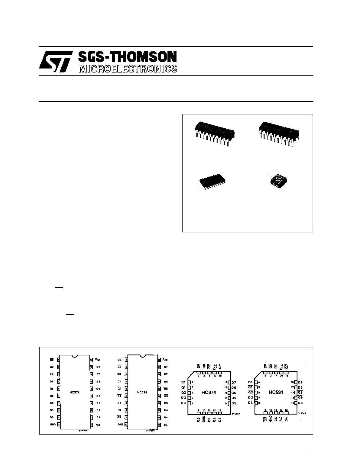
B1R
(PlasticPackage)
M1R
(MicroPackage)
ORDER CODES :
M54HC X XXF1R M74HC XXXM1R
M74HC X XXB1R M74HCXXXC1R
F1R
(CeramicPackage)
C1R
(Chip Carrier)
The M54/74HC374, M54/74HC534,arehighspeed
CMOSOCTAL D-TYPEFLIPFLOPWITH3-STATE
OUTPUTS fabricated with in silicon gate C2MOS
technology. They have the same high speed performance of LSTTLcombined with true CMOS low
power comsuption. These8-bit D-type flip-flops are
controlled byaclockinput(CK) and anouputenable
input(OE).On thepositivetransition oftheclock,the
Qoutputswillbesettothelogicstatethatweresetup
at the D inputs (HC374) or their complements
(HC534).
While the OE input is low, the eightoutputs will be
in a normal logic state (high or lowlogic level), and
PIN CONNECTION (top view)
whilehigh level, the outputs willbe in a high impedancestate.The outputcontroldoes notaffecttheinternaloperation of flip-flops.Thatis,theolddatacan
be retained or the new data can be entered even
while the outputs are off. The application engineer
has a choice of combination of inverting and non-invertingoutputs. The HC374 and HC574 areidentical, apart from pin layout. The 3-state output
configuration and the wide choice of outline make
bus-organized systems simple. All inputs are
equipped with protection circuits against static dischargeand transient excessvoltage.
March1993
1/13
M54/M74HC374/534
INPUT AND OUTPUT EQUIVALENT CIRCUIT
PIN DESC RIPTION (HC374)
PIN No SYMBOL NAME AND FUNCTION
1 OE 3 State output Enable
Input (Active LOW)
2, 5, 6, 9,
12, 15, 16,
19
3, 4, 7, 8,
13, 14, 17,
18
11 CLOCK Clock Input (LOW to
10 GND Ground (0V)
20 V
Q0 to Q7 3 State outputs
D0 to D7 Data Inputs
HIGH, edge triggered)
CC
Positive Supply Voltage
IEC LOGIC SYMBOLS
HC374 HC534
PIN DESCRIPTION (HC534)
PIN No SYMBOL NAME AND FUNCTION
1 OE 3 State output Enable
Input (Active LOW)
2, 5, 6, 9,
12, 15, 16,
19
3, 4, 7, 8,
13, 14, 17,
18
11 CLOCK Clock Input (LOW to
10 GND Ground (0V)
20 V
Q0 to Q7 3 State outputs
D0 to D7 Data Inputs
HIGH, edge triggered)
CC
Positive Supply Voltage
2/13
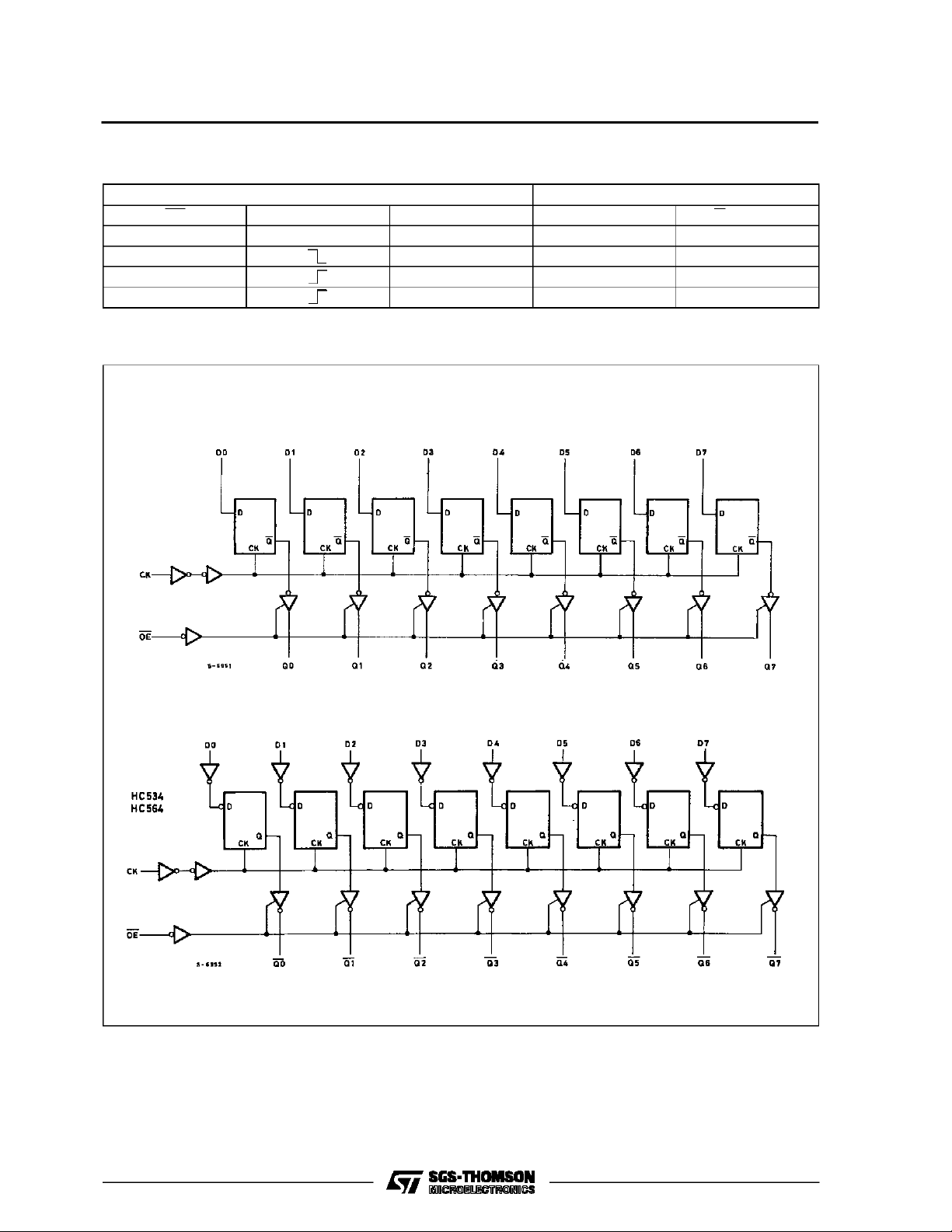
TRUTH TABLE
OE CK D Q (HC374) Q (HC534)
HXXZZ
L X NO CHANGE NO CHANGE
LLLH
LHHL
LOGIC DIAGRAMS
M54/M74HC374/534
INPUTS OUTPUTS
3/13
M54/M74HC374/534
ABSOLU TE M AXIMU M R AT ING S
Symbol Parameter Value Unit
V
CC
V
V
O
I
IK
I
OK
I
O
I
or I
CC
P
D
T
stg
T
AbsoluteMaximumRatings arethose valuesbeyond whichdamage tothedevice mayoccur. Functionaloperationunder these conditionisnotimplied.
(*)500 mW:≅ 65oC derate to 300mW by 10mW/oC: 65oCto85oC
RECO MM ENDED OPERAT I N G CO NDI TI O NS
Symbol Parameter Value Unit
V
CC
V
I
V
O
T
op
t
r,tf
Supply Voltage -0.5 to +7 V
DC Input Voltage -0.5 to VCC+ 0.5 V
I
DC Output Voltage -0.5 to VCC+ 0.5 V
DC Input Diode Current ± 20 mA
DC Output Diode Current ± 20 mA
DC Output Source Sink Current Per Output Pin ± 35 mA
DC VCCor Ground Current ± 70 mA
GND
Power Dissipation 500 (*) mW
Storage Temperature -65 to +150
Lead Temperature (10 sec) 300
L
Supply Voltage 2 to 6 V
Input Voltage 0 to V
Output Voltage 0 to V
Operating Temperature: M54HC Series
M74HC Series
CC
CC
-55 to +125
-40 to +85
Input Rise and Fall Time VCC= 2 V 0 to 1000 ns
V
= 4.5 V 0 to 500
CC
V
= 6 V 0 to 400
CC
o
C
o
C
V
V
o
C
o
C
4/13
 Loading...