

OCTAL D-TYPE LATCH WITH 3 STATE OUTPUT
HC373 NON INVERTING - HC533 INVERTING
.HIGH SPEED
tPD= 11 ns(TYP.) AT VCC=5V
.LOWPOWERDISSIPATION
ICC=4µA(MAX.) AT TA=25°C
.HIGH NOISEIMMUNITY
V
NIH=VNIL
=28%VCC(MIN.)
.OUTPUT DRIVE CAPABILITY
15 LSTTL LOADS
.SYMMETRICALOUTPUT IMPEDANCE
IOL=IOH= 6 mA (MIN.)
.BALANCEDPROPAGATION DELAYS
t
PLH=tPHL
.WIDE OPERATINGVOLTAGE RANGE
VCC(OPR)= 2V TO6 V
.PIN ANDFUNCTION COMPATIBLE
WITH 54/74LS373/533
DESCRIPTION
The M54/74HC373/533 are high speed CMOS
OCTAL LATCH WITH 3-STATE OUTPUTS
fabricated within silicon gateC2MOS technology.
These ICs achive the high speed operation similar
to equivalent LSTTL while maintaning the CMOS
low power dissipation.
These8bit D-Type latches are controlled bya latch
enable input (LE) and aoutput enable input (OE).
While the LE input is held at a high level, the Q
outputs will follow the data input precisely or
inversely. When the LE is taken low, theQ outputs
willbelatchedpreciselyorinversely atthelogiclevel
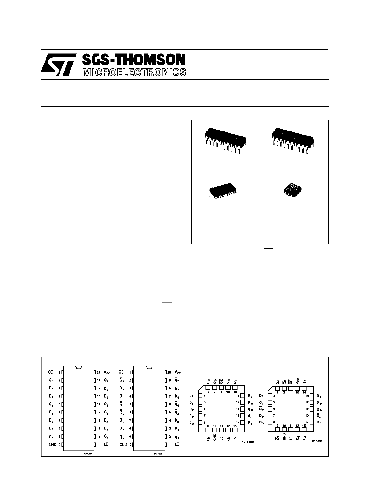
M54/74HC373
M54/ 74 HC5 33
B1R
(PlasticPackage)
M1R
(MicroPackage)
ORDER CODE S :
M54HC XXXF1R M74HC XXXM1R
M74HC XXXB1R M74H CXXXC1R
of D input data. While the OE input is at low level,
the eightoutputs willbe in anormal logic state(high
or lowlogiclevel) andwhile high levelthe outpts will
be in a high impedance state.
The application designer has a choise of
combination of inverting andnon invertingoutputs.
The three state output configuration and the wide
choise of outline make bus organized system
simple.
All inputs are equipped with protection circuits
against discharge andtransient excessvoltage.
F1R
(CeramicPackage)
C1R
(Chip Carrier)
PIN CONNECTION (top view)
HC373 HC533 HC373 HC533
October 1993
1/13
M54/M74HC373/533
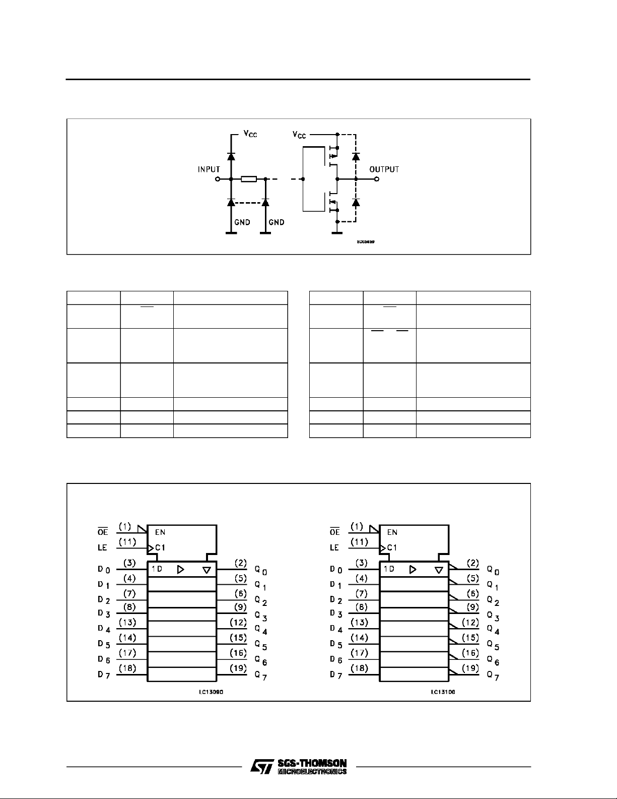
INPUT AND OUTPUT EQUIVALENT CIRCUIT
PIN DESC RIPTION (H C373)
PIN No SYMBOL NAME AND FUNCTION
1 OE 3 State output Enable
Input (Active LOW)
2, 5, 6, 9,
12, 15, 16,
19
3, 4, 7, 8,
13, 14, 17,
18
11 LE Latch Enable Input
10 GND Ground (0V)
20 V
Q0 to Q7 3 State outputs
D0 to D7 Data Inputs
CC
Positive Supply Voltage
IEC LOGIC SYMBOLS
HC373 HC533
PIN DESCRIPTION (HC533)
PIN No SYMBOL NAME AND FUNCTION
1 OE 3 State output Enable
Input (Active LOW)
2, 5, 6, 9,
12, 15, 16,
19
3, 4, 7, 8,
13, 14, 17,
18
11 LE Latch Enable Input
10 GND Ground (0V)
20 V
Q0 to Q7 3 State outputs
D0 to D7 Data Inputs
CC
Positive Supply Voltage
2/13
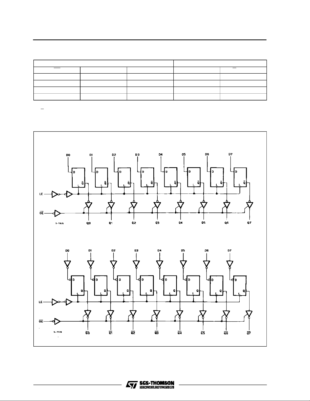
TRUTH TABLE
INPUTS OUTPUTS
OE LE D Q (HC373) Q (HC533)
HXXZZ
L L X NO CHANGE * NO CHANGE *
LHLLH
LHHHL
X: DON’T CARE
Z: HIGH IMPEDANCE
*: Q/Q OUTPUTS ARE LATCHED AT THETIMEWHENTHE LE INPUTIS TAKEN LOW LOGIC LEVEL.
LOGIC DIAGRAMS
HC373
M54/M74HC373/533
HC533
3/13
M54/M74HC373/533
ABSOLU TE M AXIMU M R AT ING S
Symbol Parameter Value Unit
V
CC
V
V
O
I
IK
I
OK
I
O
I
or I
CC
P
D
T
stg
T
AbsoluteMaximumRatingsarethosevalues beyondwhichdamage tothedevice mayoccur.Functionaloperation under these conditionsisnot implied.
(*)500 mW: ≅ 65oC derateto300 mWby 10mW/oC: 65oCto85oC
RECO MM ENDED OPERAT I N G CO NDI TI O NS
Symbol Parameter Value Unit
V
CC
V
I
V
O
T
op
t
r,tf
Supply Voltage -0.5 to +7 V
DC Input Voltage -0.5 to VCC+ 0.5 V
I
DC Output Voltage -0.5 to VCC+ 0.5 V
DC Input Diode Current ± 20 mA
DC Output Diode Current ± 20 mA
DC Output Source Sink Current Per Output Pin ± 35 mA
DC VCCor Ground Current ± 70 mA
GND
Power Dissipation 500 (*) mW
Storage Temperature -65 to +150
Lead Temperature (10sec) 300
L
Supply Voltage 2 to 6 V
Input Voltage 0 to V
Output Voltage 0 to V
Operating Temperature: M54HC Series
M74HC Series
CC
CC
-55 to +125
-40 to +85
Input Rise and Fall Time VCC= 2 V 0 to 1000 ns
V
= 4.5 V 0 to 500
CC
V
= 6 V 0 to 400
CC
o
C
o
C
V
V
o
C
o
C
4/13
 Loading...