

HC367 NON INVERTING, HC368 INVERTING
.HIGH SPEED
tPD= 11 ns(TYP.) AT VCC=5V
.LOWPOWERDISSIPATION
ICC=4µA(MAX.) AT TA=25°C
.HIGH NOISEIMMUNITY
V
NIH=VNIL
=28%VCC(MIN.)
.OUTPUT DRIVE CAPABILITY
15 LSTTL LOADS
.SYMMETRICALOUTPUT IMPEDANCE
|IOH|=IOL=6 mA(MIN.)
.BALANCEDPROPAGATION DELAYS
t
PLH=tPHL
.WIDE OPERATINGVOLTAGERANGE
VCC(OPR)= 2V TO 6 V
.PIN AND FUNCTION COMPATIBLE WITH
54/74LS367/368
M54/M74HC367
M54/M74HC368
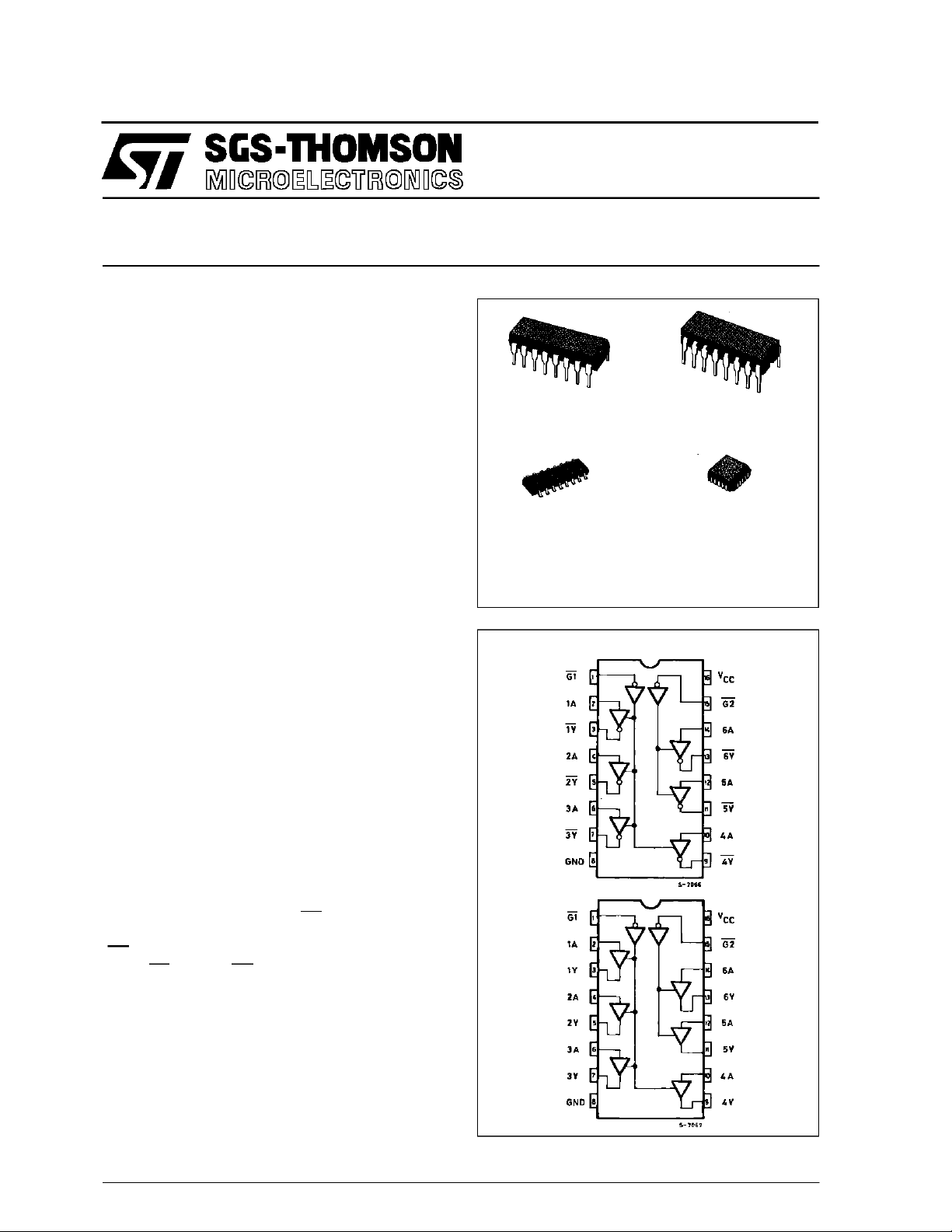
HEX BUS BUFFER(3-STATE)
B1R
(PlasticPackage)
M1R
(MicroPackage)
ORDER CODES :
M54HC X XXF 1 R M74H CXXXM1 R
M74HC X XXB1R M74H CXXXC1R
F1R
(CeramicPackage)
C1R
(Chip Carrier)
DESCRIPTION
The M54/74HC367 andtheM54/74HC368are high
speedCMOS HEXBUS BUFFER (3-STATE) fabricatedin silicongateC2MOStechnology. Theyhave
the same high speed performance of LSTTL combined with true CMOS low power consumption.
These devices contain six buffers, fourbuffers are
controlledbyan enableinput (G1)and theother two
buffers are controlled by the other enable input
(G2); theoutputs of each buffer groupare enabled
when G1 and/or G2 inputs are held low, and
when held high these outputs are disabled to be
high-impedance.
Theseoutputs arecapable ofdrivingupto15LSTTL
loads. The designer has a choice of non-inverting
outputs (HC367) and inverting outputs (HC368).
All inputs are equipped with protection circuits
against static discharge and transient excess voltage.
PIN CONNECTIONS(top view)
HC368
HC367
October 1992
1/11
M54/M74HC367/368
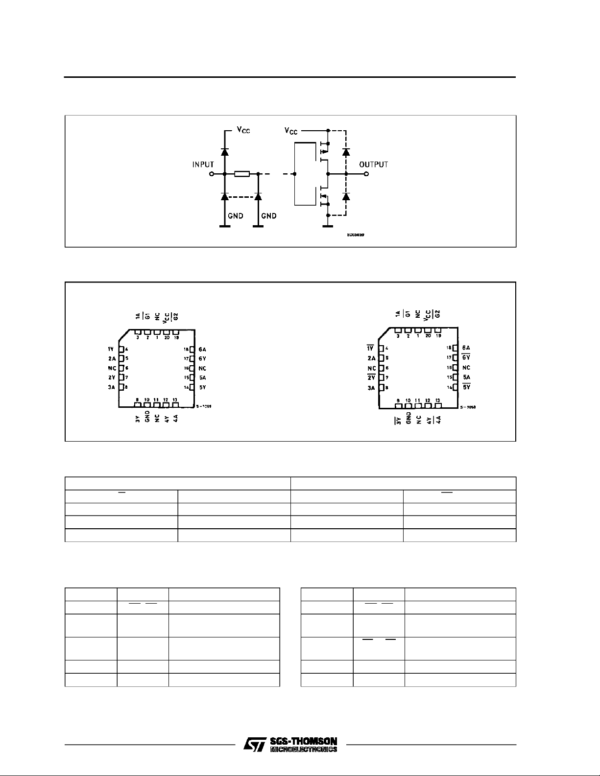
INPUT AND OUTPUT EQUIVALENT CIRCUIT
CHIP CARRIER
HC367 HC368
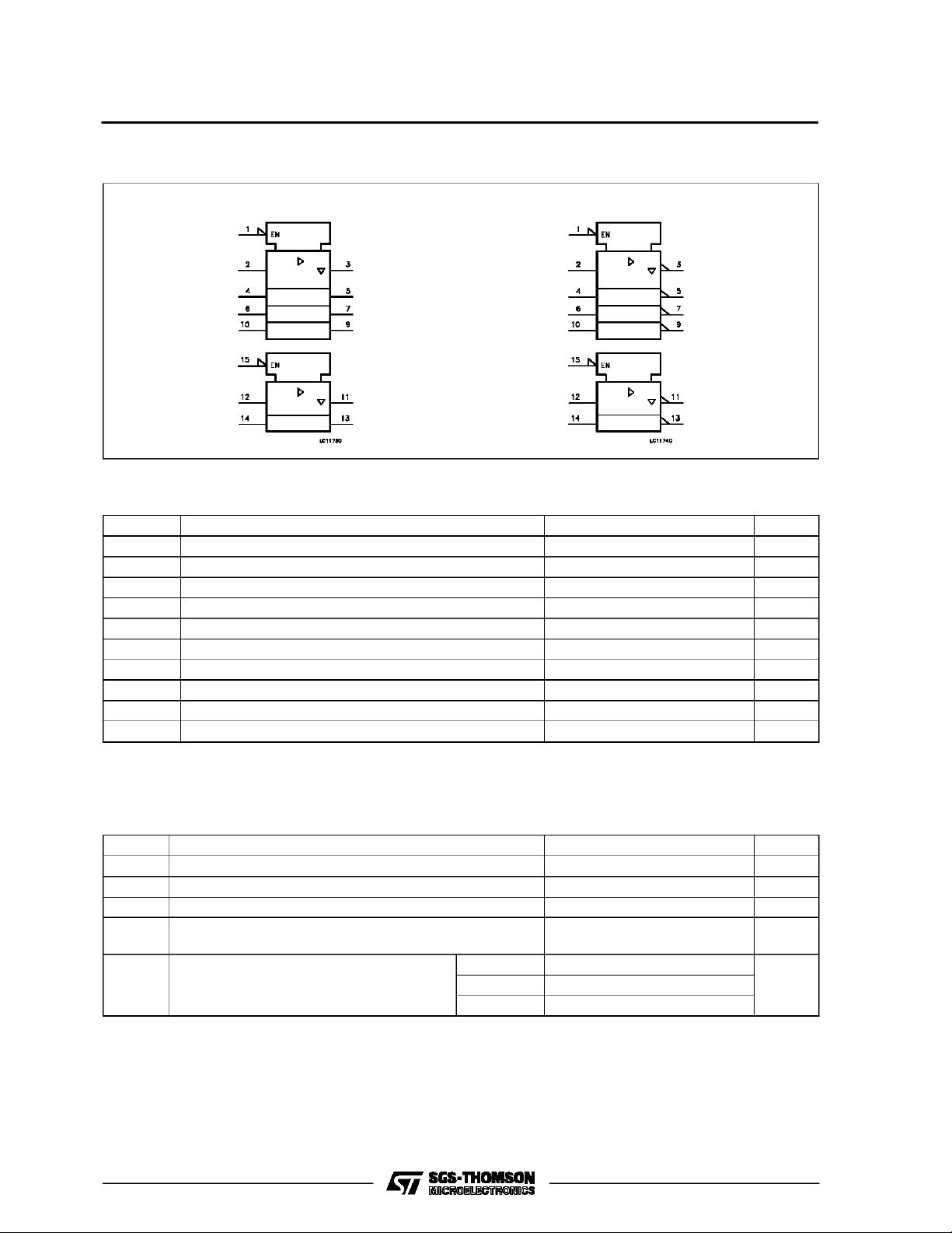
TRUTH TABLE
INPUTS OUTPUTS
G An Y n (367) Yn (368)
LLLH
LHHL
HXZZ
X = DON’T CARE Z =HIGH IMPEDANCE
PIN DESCRIPTION (HC367)
PIN No SYMBOL NAME AND FUNCTION
1, 15 G1, G2 Output Enable Inputs
2, 4, 6, 10,
12, 14
3, 5, 7, 9,
11, 13
8 GND Ground (0V)
16 V
1A to 6A Data Inputs
1Y to 6Y Data Outputs
CC
Positive Supply Voltage
NC = No Internal Connection
PIN DESCRIPTION (H C 3 68 )
PIN No SYMBOL NAME AND FUNCTION
1, 15 G1, G2 Output Enable Inputs
2, 4, 6, 10,
12, 14
3, 5, 7, 9,
11, 13
8 GND Ground (0V)
16 V
1A to 6A Data Inputs
1Y to 6Y Data Outputs
CC
Positive Supply Voltage
2/11
M54/M74HC367/368
IEC LOGIC SYMBOL
HC367 HC368
ABSOLU TE MAXI MUM RAT I NG S
Symbol Parameter Value Unit
V
CC
V
V
O
I
IK
I
OK
I
O
or I
I
CC
P
D
T
stg
T
AbsoluteMaximumRatingsarethosevalues beyondwhichdamagetothedevice mayoccur.Functionaloperationunder theseconditionisnotimplied.
(*)500 mW: ≅ 65oC derateto300 mWby 10mW/oC: 65oCto85oC
Supply Voltage -0.5 to +7 V
DC Input Voltage -0.5 to VCC+ 0.5 V
I
DC Output Voltage -0.5 to VCC+ 0.5 V
DC Input Diode Current ± 20 mA
DC Output Diode Current ± 20 mA
DC Output Source Sink CurrentPer OutputPin ± 35 mA
DC VCCor Ground Current ± 70 mA
GND
Power Dissipation 500 (*) mW
Storage Temperature -65 to +150
Lead Temperature (10 sec) 300
L
o
C
o
C
RECO MM ENDED OPERATIN G CONDITI O NS
Symbol Parameter Value Unit
V
T
t
V
V
r,tf
Supply Voltage 2 to 6 V
CC
Input Voltage 0 to V
I
Output Voltage 0 to V
O
Operating Temperature: M54HC Series
op
M74HC Series
CC
CC
-55 to +125
-40 to +85
Input Rise and Fall Time VCC= 2 V 0 to 1000 ns
V
= 4.5 V 0 to 500
CC
= 6 V 0 to 400
V
CC
V
V
o
C
o
C
3/11
M54/M74HC367/368
DC SPECIFICA TIONS
Symbol Parameter
V
V
V
V
I
I
High Level Input
IH
Voltage
Low Level Input
IL
Voltage
High Level
OH
Output Voltage
Low Level Output
OL
Voltage
I
Input Leakage
I
Current
3 State Output
OZ
Off State Current
Quiescent Supply
CC
Current
Test Conditions Value
V
(V)
CC
=25oC
A
54HC and 74HC
Min. Typ. Max. Min. Max. Min. Max.
-40 to 85oC
74HC
-55 to 125oC
54HC
Unit
T
2.0 1.5 1.5 1.5
4.5 3.15 3.15 3.15
6.0 4.2 4.2 4.2
2.0 0.5 0.5 0.5
4.5 1.35 1.35 1.35
6.0 1.8 1.8 1.8
2.0
4.5 4.4 4.5 4.4 4.4
6.0 5.9 6.0 5.9 5.9
4.5 I
6.0 I
2.0
4.5 0.0 0.1 0.1 0.1
6.0 0.0 0.1 0.1 0.1
4.5 I
6.0 I
6.0
6.0
=
V
I
IO=-20 µA
V
IH
or
V
IL
=-6.0 mA 4.18 4.31 4.13 4.10
O
=-7.8 mA 5.68 5.8 5.63 5.60
O
=
V
I
IO=20µA
V
IH
or
V
IL
= 6.0 mA 0.17 0.26 0.33 0.40
O
= 7.8 mA 0.18 0.26 0.33 0.40
O
VI=VCCor GND ±0.1 ±1 ±1 µA
VI=VIHor V
VO=VCCor GND
1.9 2.0 1.9 1.9
0.0 0.1 0.1 0.1
IL
±0.5 ±5 ±10 µA
6.0 VI=VCCor GND 4 40 80 µA
V
V
V
V
4/11

M54/M74HC367/368
AC ELECTRICAL CHARACTERISTICS (CL=50pF,Inputtr=tf=6ns)
Test Conditions Value
T
=25oC
Symbol Parameter
t
t
TLH
THL
Output Transition
Time
V
C
CC
(V)
L
(pF)
2.0
50
4.5 7121518
A
54HC and 74HC
Min. Typ. Max. Min. Max. Min. Max.
25 60 75 90
6.0 6101315
t
PLH
t
PHL
Propagation
Delay Time
2.0
50
4.5 10 17 21 26
30 85 105 130
6.0 9141822
2.0
150
4.5 14 21 26 32
42 105 130 160
6.0 12 18 22 27
t
t
PZH
PZL
Output Enable
Time
2.0
50 RL=1KΩ
4.5 11 18 23 27
36 90 115 135
6.0 9152023
2.0
150 R
4.5 15 22 28 33
=1KΩ
L
49 110 140 165
6.0 13 19 24 28
t
t
PHZ
PLZ
Output Disable
Time
2.0
50 RL=1KΩ
4.5 14 19 24 29
32 95 120 145
6.0 12 16 20 25
C
C
PD
Input Capacitance 5 10 10 10 pF
IN
(*) Power Dissipation
33
Capacitance
(*) CPDisdefined as the value ofthe IC’sinternal equivalent capacitance which is calculated fromthe operatingcurrent consumption without load.
(Referto Test Circuit).Average operting current canbe obtained bythe followingequation. ICC(opr) = CPD•VCC•fIN+ICC/6(per Channel)
-40 to 85oC
74HC
-55 to 125oC
54HC
Unit
ns
ns
ns
ns
ns
ns
pF
TEST CIRCUIT ICC(Opr.)
INPUT WAVEFORM IS THE SAME AS THAT IN CASE OF
SWITCHINGCHARACTERISTICSTEST.
CPDCALCULATION
CPDis to be calculated with the following
formula by using the measured value of
ICC(opr.) in the testcircuit opposite.
I
(
opr
CPD=
f
CC
IN
)
×
V
CC
In determining the typicalvalue of CPD,a
relatively highfrequency of 1MHzwasappliedto fIN, in order to eliminate any error
causedby the quiescent supplycurrent.
5/11

M54/M74HC367/368
SWITCHING CHARACTERISTICS TEST WAVEFORM
GND
V
CC
Note:Such a logic levelshall be appliedto eachinput that the output voltage stays in theapposite side to the switchconnection level,when
the outputis enable.
6/11

Plastic DIP16 (0.25) MECHANICAL DATA
M54/M74HC367/368
DIM.
MIN. TYP. MAX. MIN. TYP. MAX.
a1 0.51 0.020
B 0.77 1.65 0.030 0.065
b 0.5 0.020
b1 0.25 0.010
D 20 0.787
E 8.5 0.335
e 2.54 0.100
e3 17.78 0.700
F 7.1 0.280
I 5.1 0.201
L 3.3 0.130
Z 1.27 0.050
mm inch
P001C
7/11

M54/M74HC367/368
Ceramic DIP16/1 MECHANICAL DATA
DIM.
MIN. TYP. MAX. MIN. TYP. MAX.
A 20 0.787
B 7 0.276
D 3.3 0.130
E 0.38 0.015
e3 17.78 0.700
F 2.29 2.79 0.090 0.110
G 0.4 0.55 0.016 0.022
H 1.17 1.52 0.046 0.060
L 0.22 0.31 0.009 0.012
M 0.51 1.27 0.020 0.050
N 10.3 0.406
P 7.8 8.05 0.307 0.317
Q 5.08 0.200
mm inch
8/11
P053D

SO16 (Narrow)MECHANICAL DATA
M54/M74HC367/368
DIM.
MIN. TYP. MAX. MIN. TYP. MAX.
A 1.75 0.068
a1 0.1 0.2 0.004 0.007
a2 1.65 0.064
b 0.35 0.46 0.013 0.018
b1 0.19 0.25 0.007 0.010
C 0.5 0.019
c1 45° (typ.)
D 9.8 10 0.385 0.393
E 5.8 6.2 0.228 0.244
e 1.27 0.050
e3 8.89 0.350
F 3.8 4.0 0.149 0.157
G 4.6 5.3 0.181 0.208
L 0.5 1.27 0.019 0.050
M 0.62 0.024
S8°(max.)
mm inch
P013H
9/11

M54/M74HC367/368
PLCC20 MECHANICAL DATA
DIM.
MIN. TYP. MAX. MIN. TYP. MAX.
A 9.78 10.03 0.385 0.395
B 8.89 9.04 0.350 0.356
D 4.2 4.57 0.165 0.180
d1 2.54 0.100
d2 0.56 0.022
E 7.37 8.38 0.290 0.330
e 1.27 0.050
e3 5.08 0.200
F 0.38 0.015
G 0.101 0.004
M 1.27 0.050
M1 1.14 0.045
mm inch
10/11
P027A

M54/M74HC367/368
Information furnishedis believed to be accurate and reliable.However, SGS-THOMSON Microelectronics assumes no responsabilityfor the
consequences of useof such information norfor any infringementof patents or other rights of third parties which may results from its use. No
license is granted byimplication or otherwiseunder any patentor patent rightsof SGS-THOMSON Microelectronics.Specificationsmentioned
in thispublication are subjectto change without notice.This publication supersedes and replaces all information previouslysupplied.
SGS-THOMSON Microelectronicsproducts are not authorized foruse ascritical componentsin life supportdevices or systemswithout express
written approval ofSGS-THOMSON Microelectonics.
1994SGS-THOMSON Microelectronics- All Rights Reserved
Australia -Brazil - France- Germany- HongKong - Italy- Japan - Korea - Malaysia- Malta - Morocco -The Netherlands-
Singapore -Spain - Sweden - Switzerland -Taiwan -Thailand - United Kingdom -U.S.A
SGS-THOMSON Microelectronics GROUP OFCOMPANIES
11/11
 Loading...