

SGS Thomson Microelectronics M74HC356 Datasheet
8 CHANNEL MULTIPLEXER/REGISTER
.HIGH SPEED
tPD= 25 ns(TYP.) AT VCC=5V
.LOWPOWER DISSIPATION
ICC=4µA(MAX.) AT TA=25°C
.HIGH NOISE IMMUNITY
V
NIH=VNIL
=28%VCC(MIN.)
.OUTPUT DRIVE CAPABILITY
15 LSTTLLOADS
.SYMMETRICALOUTPUT IMPEDANCE
|IOH|=IOL=6 mA (MIN.)
.BALANCEDPROPAGATION DELAYS
t
PLH=tPHL
.WIDE OPERATING VOLTAGE RANGE
VCC(OPR)= 2 V TO 6 V
.PIN AND FUNCTION COMPATIBLE WITH
54/74LS356
M54HC356
M74HC356
WITH LATCHES (3-STATE)
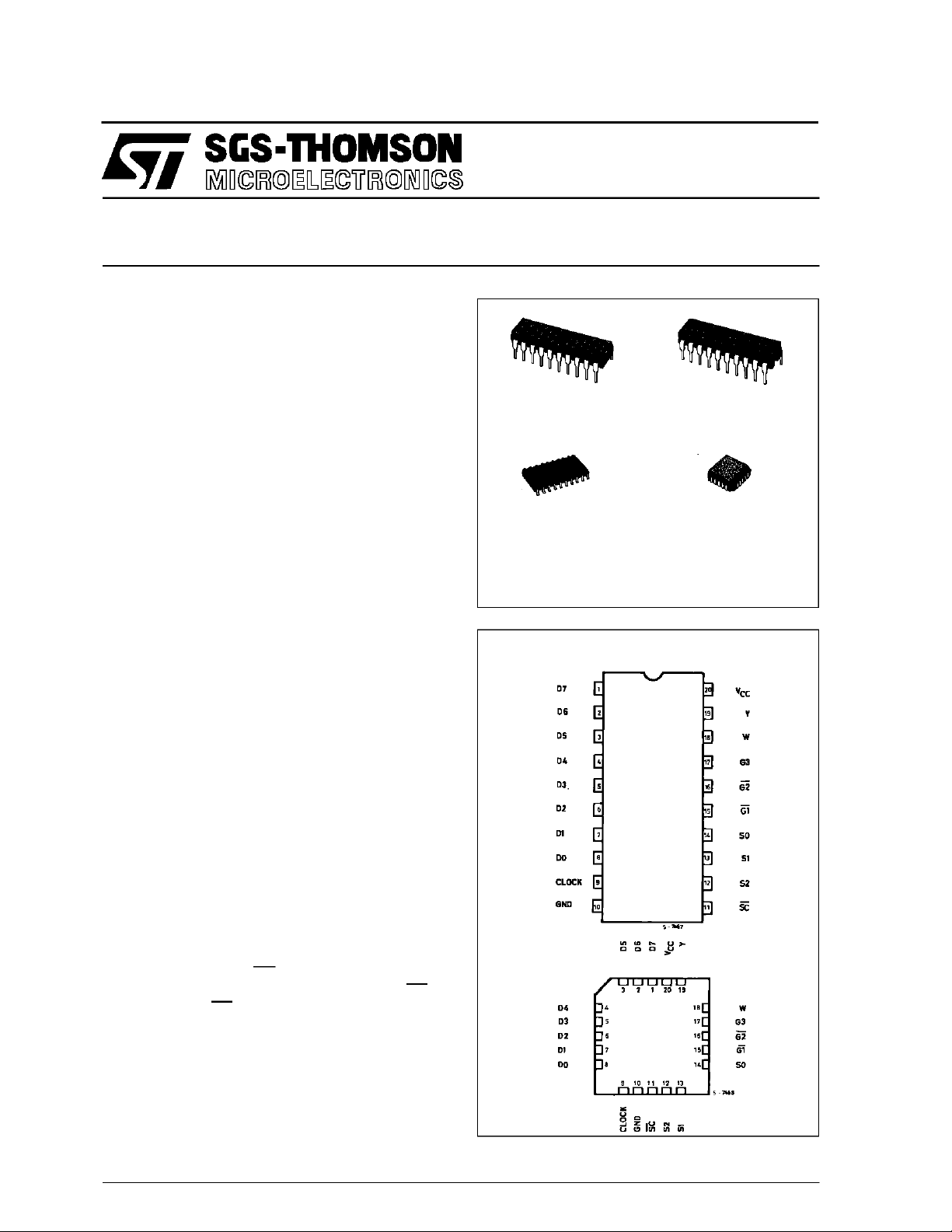
B1R
(PlasticPackage)
M1R
(MicroPackage)
ORDER CODES :
M54HC 356F1R M74H C356M1R
M74HC 356B1R M74HC3 56C1R
F1R
(CeramicPackage)
C1R
(Chip Carrier)
DESCRIPTION
TheM54/74HC356is ahighspeedCMOS8-CHANNEL MULTIPLEXER/REGISTER (3-State) fabricated in silicon gate C2MOS technology. It has the
same highspeed performance of LSTTLcombined
with true CMOS low consumption.
Thisdevicecontainsan8channeldigitalmultiplexer
with an 8-bit input data register and a 3-bit address
inputregister with 3-state outputs. The one of eight
inputdata will be provided on the Y output pin (noninverted output) and W output pin (inverted output)
is determineted by the address data.
The information at the data inputs (D0 to D7) is
storedin the 8-bit flip-flop at the positive going edge
of clock input (CLOCK). The information at the address inputs(S0 to S2) is stored inthe 3-bit latchat
the negative pulse on SC input. These outputs are
disabled to be high-impedance when input G1 is
held high, input G2 is held high or input G3 is held
low. This device is suitable for interfacing with bus
linesina busorganized system.TheM54/74HC356
issimilarinfunctiontotheM54/74HC354,whichhas
an 8-bitlatch asthe dataregister insteadof an 8-bit
flip-flop.All inputs are equipped with protection circuits against static discharge and transient excess
voltage.
PIN CONNECTIONS(top view)
NC =
No Internal
Connection
January 1993
1/12
M54/M74HC356
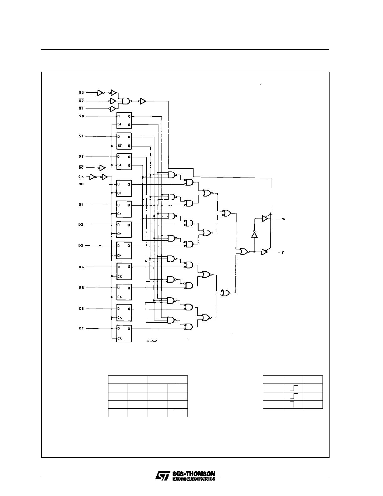
LOGIC DIAGRAM
2/12
TRUTH TABLE O F INTERNAL
LATCH
INPUTS OUTPUTS
DSTQ Q
LHLH
HHHL
X L Qn Qn
X:DON’TCARE
Qn:DATASTORED AT THE TRAILING
EDGE OF THE MOST RECENT ST
PULSE
TRUT H TABLE OF INTERNAL
LATCH (FLIP FLOP)
DCKQ
LL
HH
XQn
X: DON’TCARE
Qn: NOCHANGE
M54/M74HC356
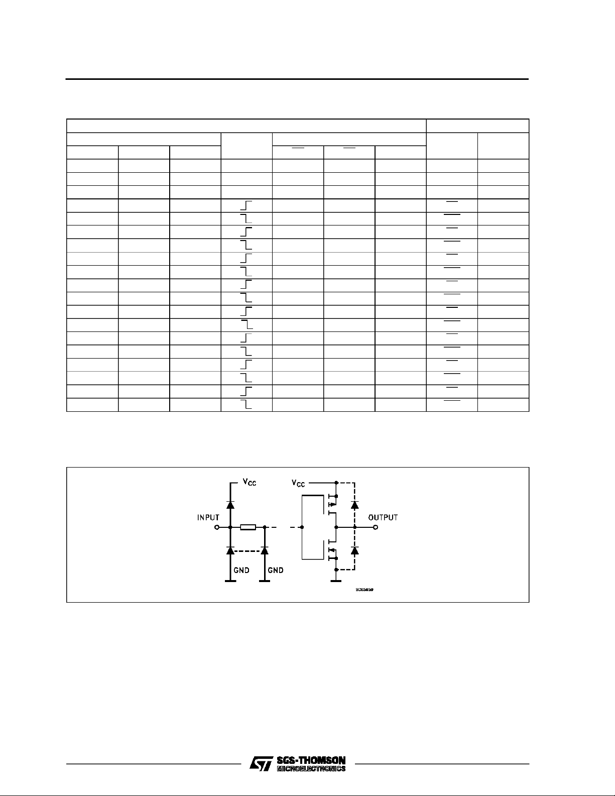
TRUTH TABLE
INPUTS
SELECT *
S2 S1 S0 G1 G2 G3
XXXXHXXZZ
XXXXXHXZZ
XXXXXXLZZ
L L L L L H D0 D0
L L L L L H D0n D0n
L L H L L H D1 D1
L L H L L H D1n D1n
LHL LLHD2D2
L H L L L H D2n D2n
L H H L L H D3 D3
L H H L L H D3n D3n
HLL LLHD4D4
H L L L L H D4n D4n
H L H L L H D5 D5
H L H L L H D5n D5n
H H L L L H D6 D6
H H L L L H D6n D6n
H H H L L H D7 D7
H H H L L H D7n D7n
X:DON’TCARE Z:HIGH IMPEDANCE *:Thiscolumn shows theinputadresssetup withSC LOW.
D1 .....D7: The levelof steady stateinputsat input D1 througthD7, respectively,at the time ofthe LOW to HIGHtransitionoftheclock.
CLOCK
OUTPUT ENABLES
WY
INPUT AND OUTPUT EQUIVALENT CIRCUIT
3/12
M54/M74HC356
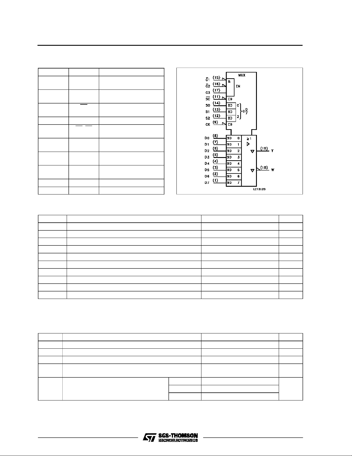
PIN DESCRIPTION
IEC LOGIC SYMBOL
PIN No SYMBOL NAME AND FUNCTION
8, 7,, 6, 5,
D0 to D7 Data Inputs
4, 3, 2, 1
9 CLOCK Clock Input (LOW to
HIGH, Edge-triggered)
11 SC Latch Enable Input
(Active LOW)
14, 13, 12 S0, S1, S2 Select Inputs
15, 16 G1, G2 Output Enable Inputs
(Active LOW)
17 G3 Output Enable Inputs
(Active HIGH)
18 W 3 State Multiplexer Output
(Active LOW)
19 Y 3 State Multiplexer Output
(Active HIGH)
10 GND Ground (0V)
20 V
CC
Positive Supply Voltage
ABSOLU TE M AXIMU M R AT ING
Symbol Parameter Value Unit
V
CC
V
V
O
I
IK
I
OK
I
O
I
or I
CC
P
D
T
stg
T
AbsoluteMaximumRatingsarethosevaluesbeyondwhichdamage tothedevicemay occur. Functionaloperationunder theseconditionisnotimplied.
(*)500 mW: ≅ 65oC derateto300 mWby 10mW/oC: 65oCto85oC
Supply Voltage -0.5 to +7 V
DC Input Voltage -0.5 to VCC+ 0.5 V
I
DC Output Voltage -0.5 to VCC+ 0.5 V
DC Input Diode Current ± 20 mA
DC Output Diode Current ± 20 mA
DC Output Source Sink Current Per Output Pin ± 35 mA
DC VCCor Ground Current ± 70 mA
GND
Power Dissipation 500 (*) mW
Storage Temperature -65 to +150
Lead Temperature (10 sec) 300
L
o
C
o
C
RECO MM ENDED OPERAT IN G CO NDITI O NS
Symbol Parameter Value Unit
4/12
V
T
t
V
V
r,tf
Supply Voltage 2 to 6 V
CC
Input Voltage 0 to V
I
Output Voltage 0 to V
O
Operating Temperature: M54HC Series
op
M74HC Series
CC
CC
-55 to +125
-40 to +85
Input Rise and Fall Time VCC= 2 V 0 to 1000 ns
V
= 4.5 V 0 to 500
CC
V
= 6 V 0 to 400
CC
V
V
o
C
o
C
 Loading...