

M54/74HC352
M54/74HC353
HC35 2: DUAL 4 CHA NNEL MUL TIPLEXE R(INV .)
HC353:DU AL 4 CH ANN EL MULTIPL EXE R 3 STATEOUTPUT(INV. )
.HIGH SPEED
tPD= 12 ns(TYP.) AT VCC=5V
.LOWPOWER DISSIPATION
ICC=4µA(MAX.) AT TA=25°C
.OUTPUTDRIVE CAPABILITY
10 LSTTL LOADS
.BALANCEDPROPAGATIONDELAYS
t
PLH=tPHL
B1R
(PlasticPackage)
F1R
(CeramicPackage)
.SYMMETRICALOUTPUT IMPEDANCE
IOL=IOH = 4 mA (MIN.)
.HIGH NOISE IMMUNITY
V
NIH=VNIL
.WIDE OPERATINGVOLTAGERANGE
VCC(OPR)= 2 V TO6 V
.PIN AND FUNCTION COMPATIBLE
WITH 54/74LS352/353
=28%VCC(MIN.)
M1R
(MicroPackage)
ORDER CODES :
M54HC X XXF1R M74H CXXXM1R
M74HC X XXB1R M 74HCXX XC1R
C1R
(Chip Carrier)
DESCRIPTION
The M54/74HC352 and M54/74HC353 are high
speedCMOSDUAL 4CHANNELMULTIPLEXERS
INVERTING fabricated with silicon gate C2MOS
technology.
Bothachieve high speed operation, similar to equivalent LSTTL while maintaining the CMOS low
power dissipation. The designer has a choice of
complementary output (HC352) and 3 stateoutput
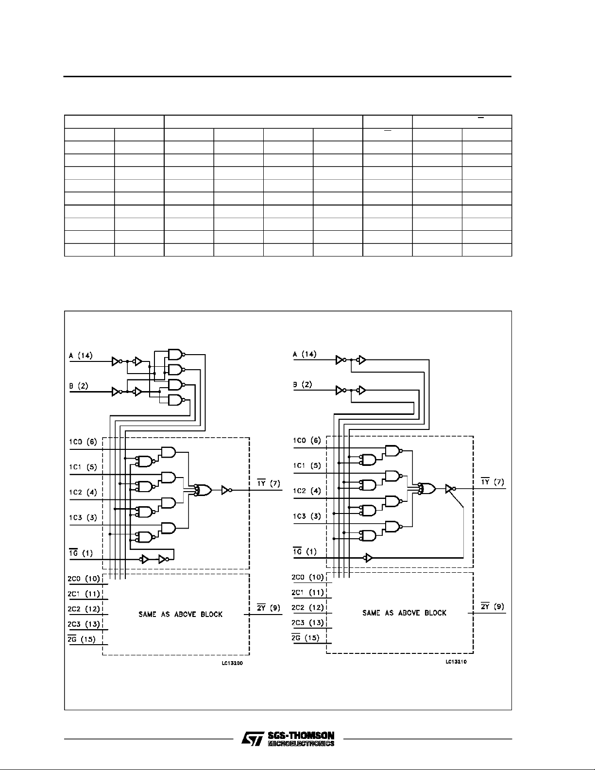
(HC353). Each of these data (1C0-1C3, 2C0-2C3)
is selected by the two addressinputs A and B.
Separate strobe inputs (1G, 2G) are provided for
eachof the twofour line sections. Taking the strobe
input(1G, 2G) high inhibitsthe outputs. The output
of HC352is fixedatlogic lowleveland theoutput of
HC353has a highimpedance, unconditionally.
All inputs are equipped with protection circuits
against static discharge and transient excess voltage.
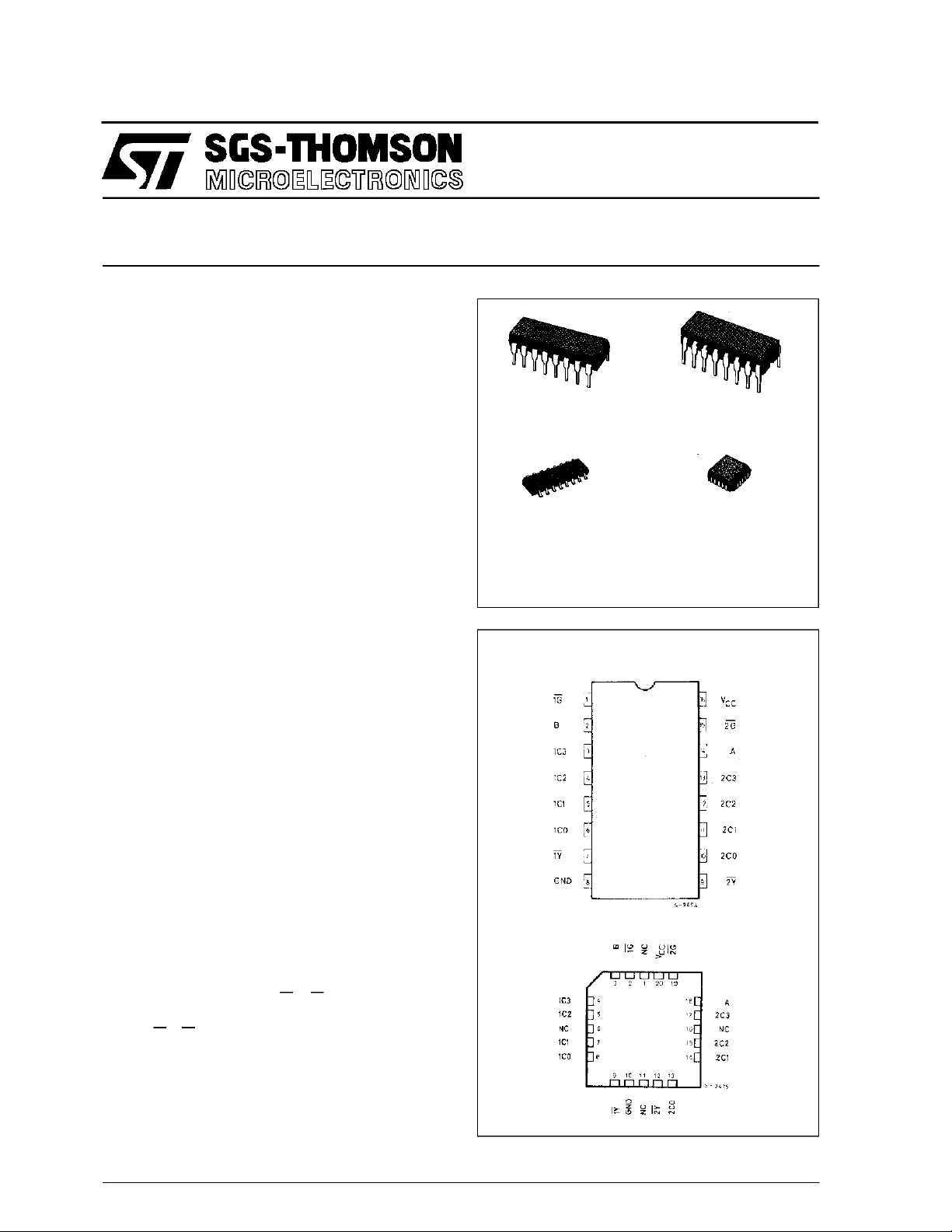
PIN CONNECTIONS(top view)
NC =
No Internal
Connection
October 1993
1/11
M54/M74HC352/353
TRUTH TABLE
SELECT INPUTS DATA INPUTS STROBE OUTPUT Y
BAC
0
XXXXXXHHZ
LLLXXXLHH
LLHXXXLLL
LHXLXXLHH
LHXHXXLL L
HLXXLXLHH
HLXXHXLLL
HHXXXLLHH
HHXXXHLLL
X:Don’t Care
Z: HighImpedance
LOGI C DIAG RAM
HC352 HC353
C
1
C
2
C
3
G HC352 HC353
2/11
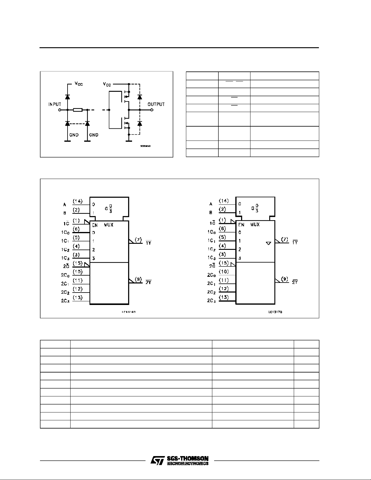
INPUT AND OUTPUT EQUIVALENT CIRCUIT PIN DESCRIPTION
PIN No SYMBOL NAME AND FUNCTION
1, 15 1G, 2G Output Enable Inputs
6, 5, 4, 3 1C
to 1C3Data Input from Source 1
0
7 1Y DataOutputs fromSource1
9 2Y DataOutputs fromSource2
10, 11, 12,132C
to 2C3Data Input from Source 2
0
14, 2 A, B Common Data Select
8 GND Ground (0V)
16 V
CC
IEC LOGIC SYMBOL
HC352 HC353
M54/M74HC352/353
Inputs
Positive Supply Voltage
ABSOLU TE M AXI MU M R AT INGS
Symbol Parameter Value Unit
V
CC
V
V
O
I
IK
I
OK
I
O
or I
I
CC
P
D
T
stg
T
AbsoluteMaximumRatingsarethosevalues beyondwhichdamage tothedevicemayoccur.Functional operationunder theseconditionisnotimplied.
(*)500 mW:≅ 65oC derateto 300 mW by 10mW/oC: 65oCto85oC
Supply Voltage -0.5 to +7 V
DC Input Voltage -0.5 to VCC+ 0.5 V
I
DC Output Voltage -0.5 to VCC+ 0.5 V
DC Input Diode Current ± 20 mA
DC Output Diode Current ± 20 mA
DC Output Source Sink Current Per Output Pin ± 25 mA
DC VCCor Ground Current ± 50 mA
GND
Power Dissipation 500 (*) mW
Storage Temperature -65 to +150
Lead Temperature (10 sec) 300
L
o
C
o
C
3/11
M54/M74HC352/353
RECO MM ENDED O PERAT IN G CONDI TIONS
Symbol Parameter Value Unit
V
V
V
T
t
r,tf
DC SPECIFICATIO NS
Symbol Parameter
V
IH
V
V
OH
V
OL
I
I
OZ
I
CC
Supply Voltage 2 to 6 V
CC
Input Voltage 0 to V
I
Output Voltage 0 to V
O
Operating Temperature: M54HC Series
op
M74HC Series
CC
CC
-55 to +125
-40 to +85
Input Rise and Fall Time VCC= 2 V 0 to 1000 ns
V
= 4.5 V 0 to 500
CC
V
= 6 V 0 to 400
CC
Test Conditions Value
V
(V)
CC
=25oC
T
A
54HC and 74HC
-40 to 85oC
74HC
-55 to 125oC
Min. Typ. Max. Min. Max. Min. Max.
High Level Input
Voltage
2.0 1.5 1.5 1.5
4.5 3.15 3.15 3.15
6.0 4.2 4.2 4.2
Low Level Input
IL
Voltage
2.0 0.5 0.5 0.5
4.5 1.35 1.35 1.35
6.0 1.8 1.8 1.8
High Level
Output Voltage
Low Level Output
Voltage
Input Leakage
I
Current
3 State Output
Off State Current
2.0
V
=
I
4.5 4.4 4.5 4.4 4.4
6.0 5.9 6.0 5.9 5.9
4.5 I
6.0 I
2.0
4.5 0.0 0.1 0.1 0.1
6.0 0.0 0.1 0.1 0.1
4.5 I
6.0 I
6.0
IO=-20 µA
V
IH
or
V
IL
=-4.0 mA 4.18 4.31 4.13 4.10
O
=-5.2 mA 5.68 5.8 5.63 5.60
O
V
=
I
IO=20µA
V
IH
or
V
IL
= 4.0 mA 0.17 0.26 0.33 0.40
O
= 5.2 mA 0.18 0.26 0.33 0.40
O
VI=VCCor GND ±0.1 ±1 ±1 µA
VI=VIHor V
6.0
VO=VCCor GND
1.9 2.0 1.9 1.9
0.0 0.1 0.1 0.1
IL
±0.5 ±5 ±10 µA
(for HC353)
Quiescent Supply
6.0 VI=VCCor GND 4 40 80 µA
Current
54HC
V
V
o
C
o
C
Unit
V
V
V
V
4/11

AC ELECTRICAL CHARACTERISTI CS (CL=50pF,Inputtr=tf=6ns)
Test Conditions Value
T
Symbol Parameter
t
TLH
t
THL
t
PLH
t
PHL
Output Transition
Time
Propagation
Delay Time
(Cn - Y)
for HC352
=25oC
V
(V)
CC
A
54HC and 74HC
Min. Typ. Max. Min. Max. Min. Max.
2.0 30 75 95 110
4.5 8151922
6.0 7131619
2.0 56 115 145 175
4.5 14 23 29 35
6.0 12 20 25 30
-40 to 85oC
74HC
M54/M74HC352/353
-55 to 125oC
54HC
Unit
ns
ns
t
t
PLH
PHL
Propagation
Delay Time
(A, B - Y)
for HC352
t
t
PLH
PHL
Propagation
Delay Time
(G - Y)
for HC352
t
PLH
t
PHL
Propagation
Delay Time
(Cn - Y)
for HC353
t
t
PLH
PHL
Propagation
Delay Time
(A, B - Y)
for HC353
t
t
PZL
PZH
Output Enable
Time (G - Y)
for HC353
t
t
PLZ
PHZ
Output Disable
Time (G - Y)
for HC353
C
C
PD
Input Capacitance 5 10 10 10 pF
IN
(*) Power Dissipation
Capacitance
(*) CPDisdefined as the value of the IC’s internal equivalent capacitance whichis calculated from the operatingcurrentconsumption without load.
(Referto TestCircuit). Average opertingcurrentcan be obtainedbythe followingequation. ICC(opr) = CPD•VCC•fIN+I
2.0 80 150 190 225
4.5 20 30 38 45
ns
6.0 17 26 33 38
2.0 40 85 105 130
4.5 10 17 21 26
ns
6.0 9141822
2.0 64 125 155 95
4.5 16 25 31 38
ns
6.0 14 21 26 32
2.0 84 150 190 225
4.5 21 30 38 45
ns
6.0 18 26 33 38
2.0
R
=1KΩ
4.5 16 23 29 35
L
64 115 145 175
ns
6.0 14 20 25 30
2.0
4.5 11 20 25 30
RL=1KΩ
44 100 125 150
ns
6.0 9172126
for HC352
for HC353
63
61
pF
CC
5/11

M54/M74HC352/353
SWITCHING CHARACTERISTICS TEST WAVEFORMS
TEST CIRCUIT ICC(Opr.)
V
OL
V
OH
6/11

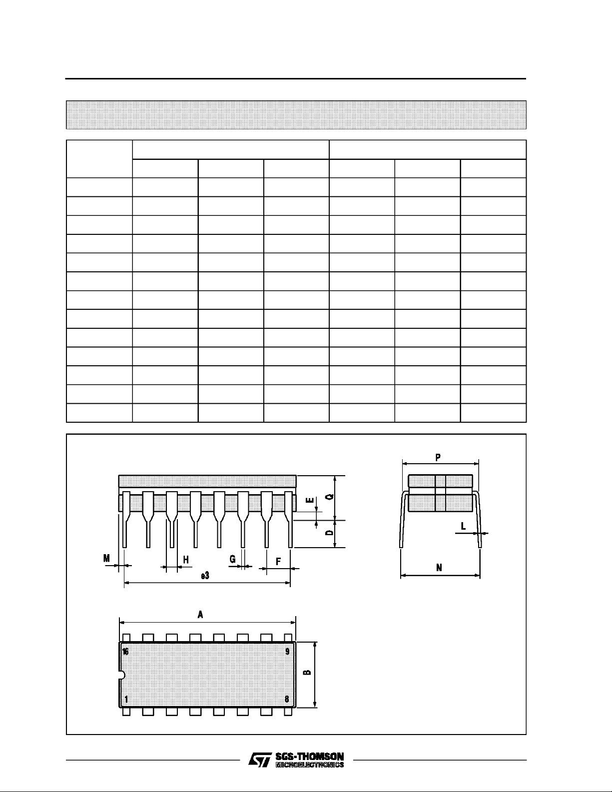
Plastic DIP16 (0.25) MECHANICAL DATA
M54/M74HC352/353
DIM.
MIN. TYP. MAX. MIN. TYP. MAX.
a1 0.51 0.020
B 0.77 1.65 0.030 0.065
b 0.5 0.020
b1 0.25 0.010
D 20 0.787
E 8.5 0.335
e 2.54 0.100
e3 17.78 0.700
F 7.1 0.280
I 5.1 0.201
L 3.3 0.130
Z 1.27 0.050
mm inch
P001C
7/11
M54/M74HC352/353
Ceramic DIP16/1 MECHANICAL DATA
DIM.
MIN. TYP. MAX. MIN. TYP. MAX.
A 20 0.787
B 7 0.276
D 3.3 0.130
E 0.38 0.015
e3 17.78 0.700
F 2.29 2.79 0.090 0.110
G 0.4 0.55 0.016 0.022
H 1.17 1.52 0.046 0.060
L 0.22 0.31 0.009 0.012
M 0.51 1.27 0.020 0.050
N 10.3 0.406
P 7.8 8.05 0.307 0.317
Q 5.08 0.200
mm inch
8/11
P053D

SO16 (Narrow) MECHANICAL DATA
M54/M74HC352/353
DIM.
MIN. TYP. MAX. MIN. TYP. MAX.
A 1.75 0.068
a1 0.1 0.2 0.004 0.007
a2 1.65 0.064
b 0.35 0.46 0.013 0.018
b1 0.19 0.25 0.007 0.010
C 0.5 0.019
c1 45° (typ.)
D 9.8 10 0.385 0.393
E 5.8 6.2 0.228 0.244
e 1.27 0.050
e3 8.89 0.350
F 3.8 4.0 0.149 0.157
G 4.6 5.3 0.181 0.208
L 0.5 1.27 0.019 0.050
M 0.62 0.024
S8°(max.)
mm inch
P013H
9/11

M54/M74HC352/353
PLCC20 MECHANICAL DATA
DIM.
MIN. TYP. MAX. MIN. TYP. MAX.
A 9.78 10.03 0.385 0.395
B 8.89 9.04 0.350 0.356
D 4.2 4.57 0.165 0.180
d1 2.54 0.100
d2 0.56 0.022
E 7.37 8.38 0.290 0.330
e 1.27 0.050
e3 5.08 0.200
F 0.38 0.015
G 0.101 0.004
M 1.27 0.050
M1 1.14 0.045
mm inch
10/11
P027A

M54/M74HC352/353
Information furnished is believed to be accurate and reliable.However, SGS-THOMSON Microelectronics assumes no responsability for the
consequences of useof such information norfor any infringementof patents or other rights of third parties which may results from its use. No
license is granted by implication orotherwise under any patentor patentrights ofSGS-THOMSON Microelectronics. Specificationsmentioned
in this publication are subject to changewithout notice. This publication supersedes and replaces allinformation previously supplied.
SGS-THOMSON Microelectronicsproductsare notauthorizedforuse ascritical componentsinlife supportdevices or systemswithoutexpress
written approval of SGS-THOMSON Microelectonics.
1994SGS-THOMSON Microelectronics - All RightsReserved
Australia -Brazil - France- Germany - HongKong - Italy- Japan - Korea - Malaysia- Malta - Morocco - The Netherlands-
Singapore -Spain - Sweden - Switzerland -Taiwan - Thailand - United Kingdom - U.S.A
SGS-THOMSON Microelectronics GROUP OF COMPANIES
11/11
 Loading...