

.HIGH SPEED
tPD= 15 ns(TYP.) at VCC=5V
.LOWPOWERDISSIPATION
ICC=4µA(MAX.) at TA=25°C
.HIGH NOISEIMMUNITY
V
NIH=VNIL
=28%VCC(MIN.)
.OUTPUT DRIVE CAPABILITY
10 LSTTL LOADS
.SYMMETRICALPROPAGATIONDELAYS
IOH =IOL= 4 mA (MIN.)
.BALANCEDPRORAGATION DELAYS
t
PLH=tPHL
.WIDE OPERATINGVOLTAGE RANGE
VCC(OPR)= 2V to 6V
.PIN AND FUNCTION COMPATIBLE WITH
54/74LS259
DESCRIPTION
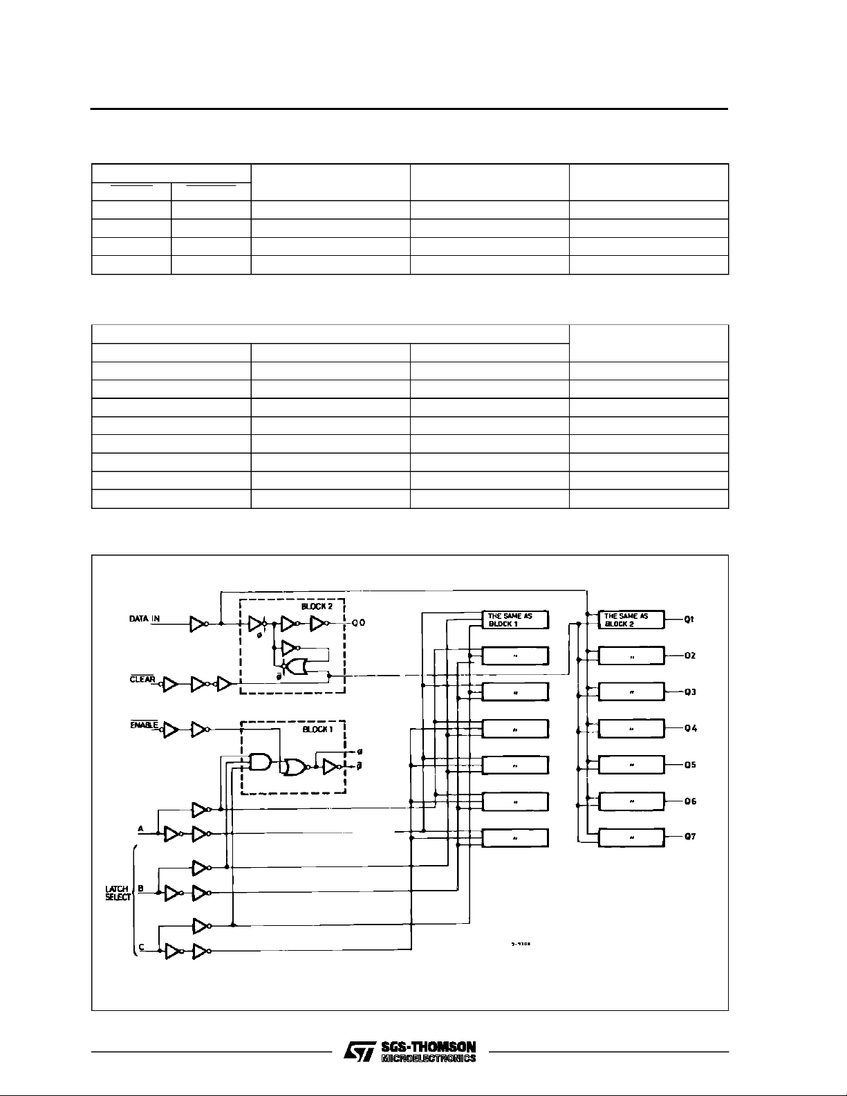
The M54/74HC259 is a high speed CMOS 8 BIT
ADDRESSABLE LATCH fabricated in silicon gate
C2MOStechnology. Ithasthesamehighspeedperformance of LSTTL combined with true CMOS low
powerconsumption.
The M54HC259/M74HC259 has single data input
(D) 8latch outputs (Q0-Q7), 3address inputs (A,B,
and C), common enable input (E), and a common
CLEARinput.Tooperate thisdeviceasan addressable latch, data is held on the D input, and the addressof thelatchintowhichthedata isto beentered
is held on the A,B,and C inputs. WhenENABLE is
taken low the data flows through to the addresses
output. The data is stored on the positive-going
edgeofthe ENABLE pulse.Allunaddressed latches
will remain unaffected. With ENABLE in the high
statethedeviceisdeselected and alllatchesremain
intheirprevious state,unaffected bychanges onthe
data or address inputs. To eliminate the possibility
of entering erroneous datainto the latches, the ENABLE should be held high (inactive) while the addresslinesarechanging. IfENABLE isheldhighand
CLEARis takenlow alleight latches are cleared to
the lowstate.IfENABLE islowall latchesexceptthe
addressed latch will be cleared. The addressed
latchwillinsteadfollowthe Dinput,effectively implementing a 3-to 8 line decoder.
All inputs are equipped with protection circuits
against static discharge and transient excess
voltage.
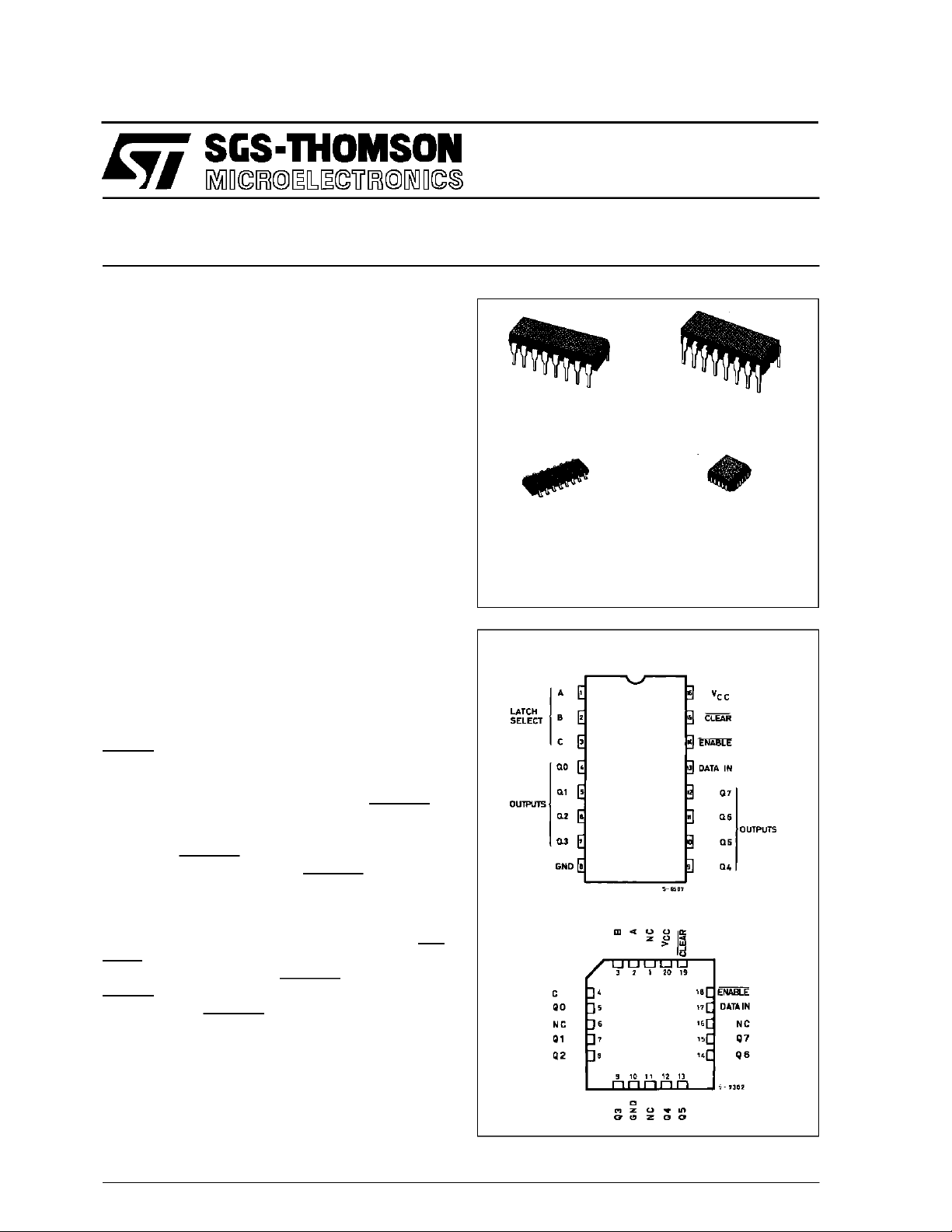
M54HC259
M74HC259
8 BIT ADDRESSABLE LATCH
B1R
(PlasticPackage)
M1R
(MicroPackage)
ORDER CODES :
M54HC 259F1R M74H C259M1R
M74HC 259B1R M74HC2 59C1R
PIN CONNECTIONS(top view)
NC =
No Internal
Connection
F1R
(CeramicPackage)
C1R
(Chip Carrier)
October 1992
1/12
M54/M74HC259
TRUTH TABLE
INPUTS OUTPUTS OF
CLEAR ENABLE
H L D Qi0 ADDRESSABLE LATCH
H H Qi0 Qi0 MEMORY
L L D L 8 LINE DEMULTIPLEXER
L H L L CLEAR ALL BITS TO ’L’
D: The level at the datainput
Qi0:The level before the indicatedsteady state input conditions wereestablished, (i = 0, 1, .....,7).
CBA
LLLQ0
LLHQ1
LHLQ2
LHHQ3
HLLQ4
HLHQ5
HHLQ6
HHHQ7
ADDRESSED LATCH
SELECT INPUTS
EACH OTHER
OUTPUT
FUNCTION
LATCH ADDRESSED
LOGI C DI AGRAM
2/12
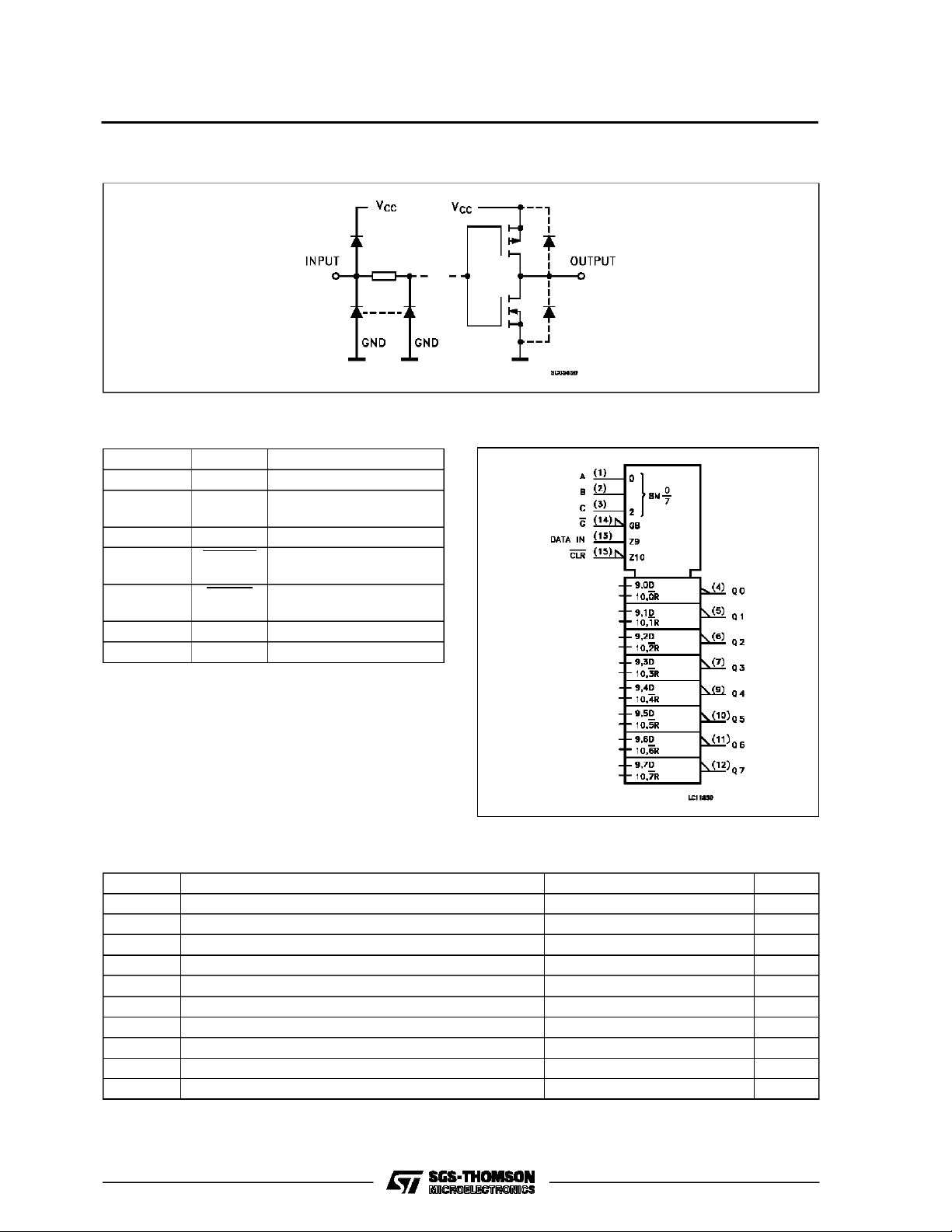
INPUT AND OUTPUT EQUIVALENT CIRCUIT
M54/M74HC259
PIN DESC RIPTION
PIN No SYMBOL NAME AND FUNCTION
1, 2, 3 A, B, C Address Inputs
4, 5, 6, 7, 9,
Q0 to Q7 Latch Outputs
10, 11, 12
13 D Data Input
14 ENABLE Latch Enable Input
(Active LOW)
15 CLEAR Conditional Reset Input
(Active LOW)
8 GND Ground (0V)
16 V
CC
Positive Supply Voltage
ABSOLU TE M AXIMU M R AT INGS
IEC LOGIC SYMBOL
Symbol Parameter Value Unit
V
CC
V
V
O
I
IK
I
OK
I
O
or I
I
CC
P
D
T
stg
T
L
AbsoluteMaximumRatingsarethose values beyondwhichdamage tothedevicemayoccur. Functionaloperationunder these conditionisnotimplied.
(*)500 mW: ≅ 65oC derateto300mWby 10mW/oC: 65oCto85oC
Supply Voltage -0.5 to +7 V
DC Input Voltage -0.5 to VCC+ 0.5 V
I
DC Output Voltage -0.5 to VCC+ 0.5 V
DC Input Diode Current ± 20 mA
DC Output Diode Current ± 20 mA
DC Output Source Sink Current Per Output Pin ± 25 mA
DC VCCor Ground Current ± 50 mA
GND
Power Dissipation 500 (*) mW
Storage Temperature -65 to +150
Lead Temperature (10sec) 300
o
C
o
C
3/12
M54/M74HC259
RECO MM ENDED OPERAT I N G CO NDI TIONS
Symbol Parameter Value Unit
V
V
V
T
t
r,tf
DC SPECIFICATIONS
Symbol Parameter
V
IH
V
V
OH
V
OL
I
I
CC
Supply Voltage 2 to 6 V
CC
Input Voltage 0 to V
I
Output Voltage 0 to V
O
Operating Temperature: M54HC Series
op
M74HC Series
CC
CC
-55 to +125
-40 to +85
Input Rise and Fall Time VCC= 2 V 0 to 1000 ns
V
= 4.5 V 0 to 500
CC
V
= 6 V 0 to 400
CC
Test Conditions Value
V
(V)
CC
=25oC
T
A
54HC and 74HC
-40 to 85oC
74HC
-55 to 125oC
Min. Typ. Max. Min. Max. Min. Max.
High Level Input
Voltage
2.0 1.5 1.5 1.5
4.5 3.15 3.15 3.15
6.0 4.2 4.2 4.2
Low Level Input
IL
Voltage
2.0 0.5 0.5 0.5
4.5 1.35 1.35 1.35
6.0 1.8 1.8 1.8
High Level
Output Voltage
Low Level Output
Voltage
Input Leakage
I
Current
Quiescent Supply
2.0
V
=
I
4.5 4.4 4.5 4.4 4.4
6.0 5.9 6.0 5.9 5.9
4.5 I
6.0 I
2.0
4.5 0.0 0.1 0.1 0.1
6.0 0.0 0.1 0.1 0.1
4.5 I
6.0 I
6.0
IO=-20 µA
V
IH
or
V
IL
=-4.0 mA 4.18 4.31 4.13 4.10
O
=-5.2 mA 5.68 5.8 5.63 5.60
O
V
=
I
IO=20µA
V
IH
or
V
IL
= 4.0 mA 0.17 0.26 0.33 0.40
O
= 5.2 mA 0.18 0.26 0.33 0.40
O
VI=VCCor GND ±0.1 ±1 ±1 µA
1.9 2.0 1.9 1.9
0.0 0.1 0.1 0.1
6.0 VI=VCCor GND 4 40 80 µA
Current
54HC
V
V
o
C
o
C
Unit
V
V
V
V
4/12
 Loading...