

.HIGH SPEED
tPD= 14 ns(TYP.) AT VCC=5V
.LOWPOWER DISSIPATION
ICC=4µA(MAX.) AT TA=25°C
.HIGH NOISEIMMUNITY
V
NIH=VNIL
=28%VCC(MIN.)
.OUTPUT DRIVE CAPABILITY
10 LSTTL LOADS
.SYMMETRICAL OUTPUT IMPEDANCE
|IOH|=IOL=4 mA (MIN.)
.BALANCEDPROPAGATION DELAYS
t
PLH=tPHL
.WIDE OPERATING VOLTAGE RANGE
VCC(OPR)= 2 V TO 6 V
.PIN AND FUNCTION COMPATIBLE
WITH 54/74LS238
M54HC238
M74HC238
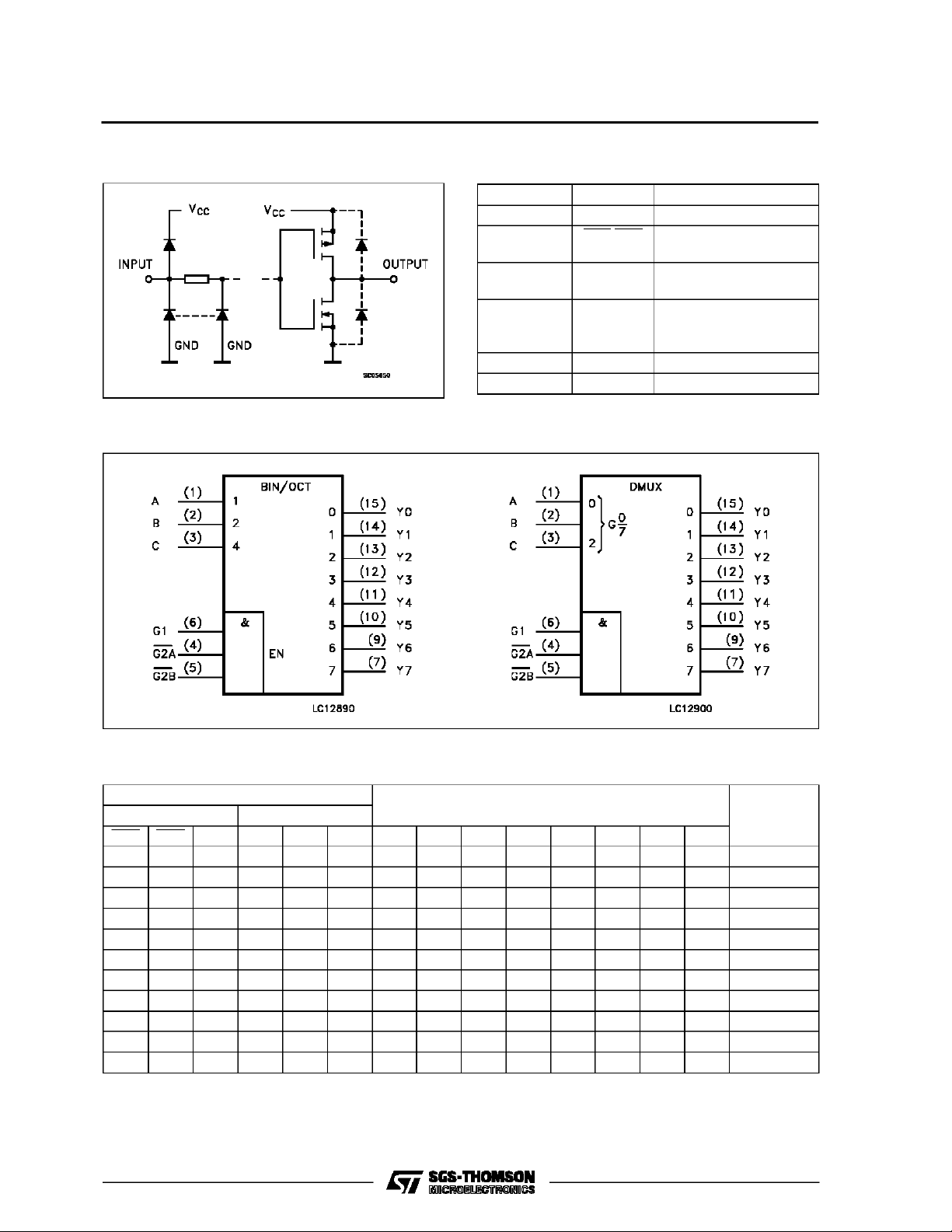
3 TO 8 LINE DECODER
B1R
(PlasticPackage)
M1R
(MicroPackage)
ORDER CODES :
M54HC 238F1R M74H C238M1R
M74HC 238B1R M74HC2 38C1R
F1R
(CeramicPackage)
C1R
(Chip Carrier)
DESCRIPTION
TheM54/74HC238 is ahigh speed CMOS3 to8 line
decoderfabricated insilicongateC2MOStechnology.
It has the same high speed performance of LSTTL
combined with trueCMOSlowpower consumption.If
thedeviceisenabled,3 binary selectinputs(A,B and
C)determinewhichoneofoutputswillgohigh.Enable
inputG1 is held ”Low” or either G2A or G2B is held
”High” decoding function isinhibited andallthe 8 outputsgolow.Three enable inputs areprovided toease
cascade connection and application of this address
decoder inmemory systems.
Allinputs areequipped with protectioncircuitsagainst
staticdischarge and transient excess voltage.
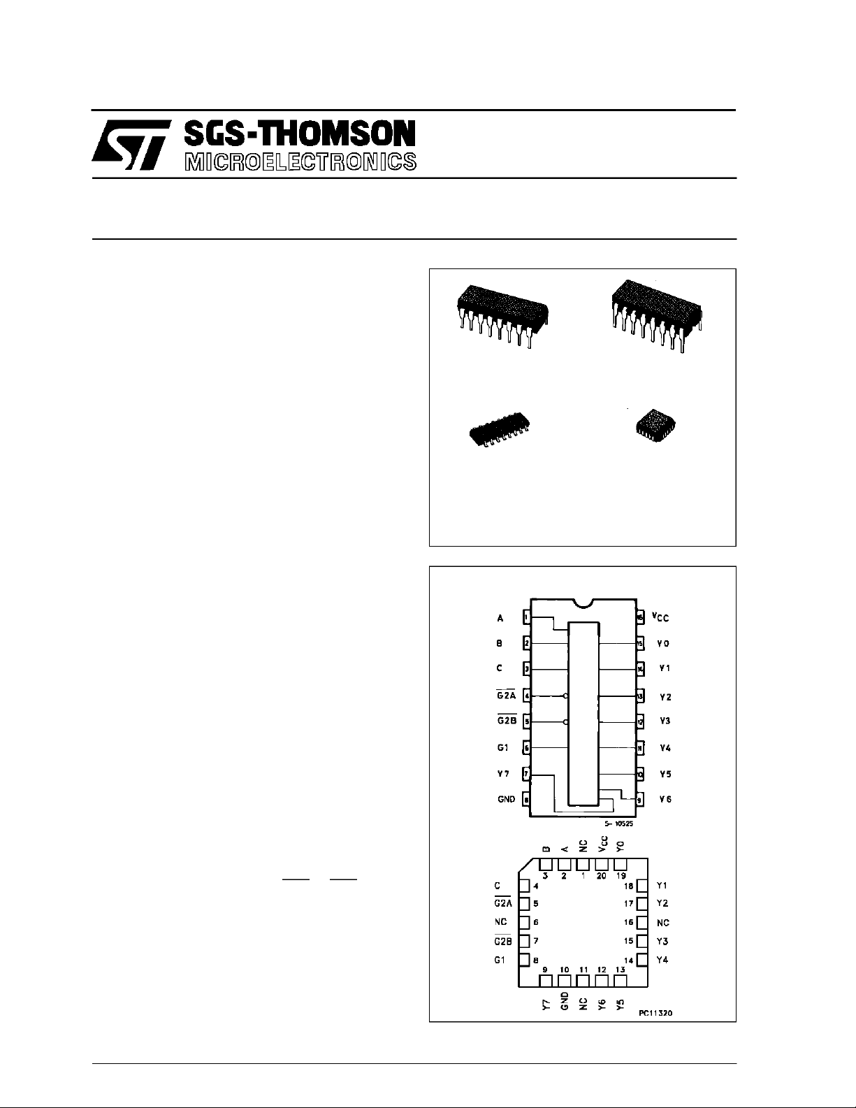
NC =
No Internal
Connection
PIN CONNECTIONS(top view)
October 1993
1/10
M54/M74HC238
INPUT AND OUTPUT EQUIVALENT CIRCUIT
IEC LOGIC SYMBOLS
PIN DESCRIPTION
PIN No SYMBOL NAME AND FUNCTION
1, 2, 3 A, B, C Data Inputs
4, 5 G2A G2B Enable Input (Active
LOW)
6 G1 Data Enable Input
(Active HIGH)
15, 14, 13,
12, 11, 10, 9,
7
8 GND Ground (0V)
16 V
Y0 to Y7 Outputs
CC
Positive Supply Voltage
TRUTH TABLE
INPUTS
ENABLE SELECT
G2B G2A G1 C B A Y0 Y1 Y2 Y3 Y4 Y5 Y6 Y7
XXLXXXLLLLLLLL NONE
XHXXXXLLLLLLLL NONE
HXXXXXLLLLLLLL NONE
LLHLLLHLLLLLLL Y0
LLHLLHLHLLLLLL Y1
LLHLHLLLHLLLLL Y2
LLHLHHLLLHLLLL Y3
LLHHLLLLLLHLLL Y4
LLHHLHLLLLLHLL Y5
LLHHHLLLLLLLHL Y6
LLHHHHLLLLLLLH Y7
X: Don’tCare
2/10
OUTPUS SELECTED
OUTPUT
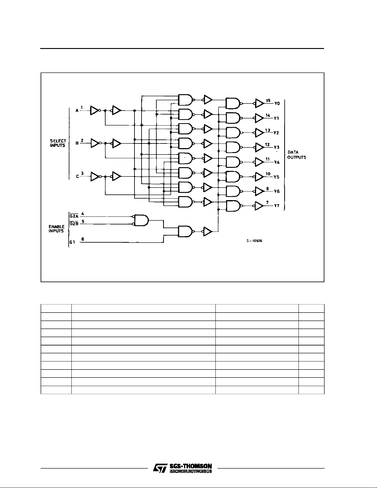
LOGIC DIAGRAM
M54/M74HC238
ABSOLU TE MAXIMUM RATING S
Symbol Parameter Value Unit
V
CC
V
V
O
I
IK
I
OK
I
O
I
or I
CC
P
D
T
stg
T
AbsoluteMaximumRatingsarethose values beyond whichdamage tothedevice mayoccur. Functionaloperation under theseconditionisnotimplied.
(*)500 mW: ≅ 65oC derateto300 mW by 10mW/oC: 65oCto85oC
Supply Voltage -0.5 to +7 V
DC Input Voltage -0.5 to VCC+ 0.5 V
I
DC Output Voltage -0.5 to VCC+ 0.5 V
DC Input Diode Current ± 20 mA
DC Output Diode Current ± 20 mA
DC Output Source Sink Current Per Output Pin ± 25 mA
DC VCCor Ground Current ± 50 mA
GND
Power Dissipation 500 (*) mW
Storage Temperature -65 to +150
Lead Temperature (10 sec) 300
L
o
C
o
C
3/10

M54/M74HC238
RECO MM ENDED OPERAT IN G C ONDITIONS
Symbol Parameter Value Unit
V
V
V
T
t
r,tf
DC SPECIFICATIO NS
Symbol Parameter
V
IH
V
V
OH
V
OL
I
I
CC
Supply Voltage 2 to 6 V
CC
Input Voltage 0 to V
I
Output Voltage 0 to V
O
Operating Temperature: M54HC Series
op
M74HC Series
CC
CC
-55 to +125
-40 to +85
Input Rise and Fall Time VCC= 2 V 0 to 1000 ns
V
= 4.5 V 0 to 500
CC
V
= 6 V 0 to 400
CC
Test Conditions Value
T
High Level Input
Voltage
=25oC
V
(V)
CC
A
54HC and 74HC
Min. Typ. Max. Min. Max. Min. Max.
2.0 1.5 1.5 1.5
4.5 3.15 3.15 3.15
-40 to 85oC
74HC
-55 to 125oC
6.0 4.2 4.2 4.2
Low Level Input
IL
Voltage
2.0 0.5 0.5 0.5
4.5 1.35 1.35 1.35
6.0 1.8 1.8 1.8
High Level
Output Voltage
Low Level Output
Voltage
Input Leakage
I
Current
Quiescent Supply
2.0
V
=
I
4.5 4.4 4.5 4.4 4.4
6.0 5.9 6.0 5.9 5.9
4.5 I
6.0 I
2.0
4.5 0.0 0.1 0.1 0.1
6.0 0.0 0.1 0.1 0.1
4.5 I
6.0 I
6.0
IO=-20 µA
V
IH
or
V
IL
=-4.0 mA 4.18 4.31 4.13 4.10
O
=-5.2 mA 5.68 5.8 5.63 5.60
O
=
V
I
IO=20µA
V
IH
or
V
IL
= 4.0 mA 0.17 0.26 0.33 0.40
O
= 5.2 mA 0.18 0.26 0.33 0.40
O
VI=VCCor GND ±0.1 ±1 ±1 µA
1.9 2.0 1.9 1.9
0.0 0.1 0.1 0.1
6.0 VI=VCCor GND 4 40 80 µA
Current
54HC
V
V
o
C
o
C
Unit
V
V
V
V
4/10

M54/M74HC238
AC ELECTRICAL CHARACTERISTICS (CL=50pF,Inputtr=tf=6ns)
Test Conditions Value
=25oC
T
Symbol Parameter
t
t
TLH
THL
Output Transition
Time
V
CC
(V)
2.0 30 75 95 110
4.5 8151922
A
54HC and 74HC
Min. Typ. Max. Min. Max. Min. Max.
6.0 7131619
t
PLH
t
PHL
t
PLH
t
PHL
t
PLH
t
PHL
C
C
PD
Propagation
Delay Time
(A, B, C - Y)
Propagation
Delay Time
(G1 - Y)
Propagation
Delay Time
(G2 - Y)
Input Capacitance 5 10 10 10 pF
IN
(*) Power Dissipation
2.0 50 150 190 225
4.5 17 30 38 45
6.0 15 26 32 38
2.0 50 150 190 225
4.5 17 30 38 45
6.0 15 26 32 38
2.0 50 150 190 225
4.5 17 30 38 45
6.0 15 26 32 38
53
Capacitance
(*) CPDisdefinedas the value ofthe IC’sinternal equivalent capacitance which is calculated from the operating current consumption without load.
(RefertoTest Circuit).Average opertingcurrentcan be obtained by thefollowingequation. ICC(opr) = CPD•VCC•fIN+I
-40 to 85oC
74HC
-55 to 125oC
54HC
CC
Unit
ns
ns
ns
ns
pF
WAVEFORM
TEST CIRCUIT ICC(Opr.)SWITCHING CHARACTERISTICS TEST
INPUT WAVEFORM IS THE SAME AS THAT IN CASE OF
SWITCHINGCHARACTERISTICSTEST.
5/10

M54/M74HC238
Plastic DIP16 (0.25) MECHANICAL DATA
DIM.
MIN. TYP. MAX. MIN. TYP. MAX.
a1 0.51 0.020
B 0.77 1.65 0.030 0.065
b 0.5 0.020
b1 0.25 0.010
D 20 0.787
E 8.5 0.335
e 2.54 0.100
e3 17.78 0.700
F 7.1 0.280
I 5.1 0.201
L 3.3 0.130
Z 1.27 0.050
mm inch
6/10
P001C

Ceramic DIP16/1 MECHANICAL DATA
M54/M74HC238
DIM.
MIN. TYP. MAX. MIN. TYP. MAX.
A 20 0.787
B 7 0.276
D 3.3 0.130
E 0.38 0.015
e3 17.78 0.700
F 2.29 2.79 0.090 0.110
G 0.4 0.55 0.016 0.022
H 1.17 1.52 0.046 0.060
L 0.22 0.31 0.009 0.012
M 0.51 1.27 0.020 0.050
N 10.3 0.406
P 7.8 8.05 0.307 0.317
Q 5.08 0.200
mm inch
P053D
7/10

M54/M74HC238
SO16 (Narrow) MECHANICAL DATA
DIM.
MIN. TYP. MAX. MIN. TYP. MAX.
A 1.75 0.068
a1 0.1 0.2 0.004 0.007
a2 1.65 0.064
b 0.35 0.46 0.013 0.018
b1 0.19 0.25 0.007 0.010
C 0.5 0.019
c1 45° (typ.)
D 9.8 10 0.385 0.393
E 5.8 6.2 0.228 0.244
e 1.27 0.050
e3 8.89 0.350
F 3.8 4.0 0.149 0.157
G 4.6 5.3 0.181 0.208
L 0.5 1.27 0.019 0.050
M 0.62 0.024
S8°(max.)
mm inch
8/10
P013H

PLCC20 MECHANICAL DATA
M54/M74HC238
DIM.
MIN. TYP. MAX. MIN. TYP. MAX.
A 9.78 10.03 0.385 0.395
B 8.89 9.04 0.350 0.356
D 4.2 4.57 0.165 0.180
d1 2.54 0.100
d2 0.56 0.022
E 7.37 8.38 0.290 0.330
e 1.27 0.050
e3 5.08 0.200
F 0.38 0.015
G 0.101 0.004
M 1.27 0.050
M1 1.14 0.045
mm inch
P027A
9/10

M54/M74HC238
Information furnished is believed tobe accurate and reliable. However, SGS-THOMSON Microelectronics assumes no responsability for the
consequences of use of such information nor for any infringementof patents or other rights of third parties which may results from its use. No
license is granted byimplication or otherwise under any patent or patent rights of SGS-THOMSON Microelectronics. Specificationsmentioned
in this publicationare subject to changewithout notice. This publication supersedes and replaces all information previously supplied.
SGS-THOMSON Microelectronicsproductsare notauthorized foruse ascritical componentsinlife support devicesorsystems withoutexpress
written approval of SGS-THOMSONMicroelectonics.
1994SGS-THOMSON Microelectronics- All RightsReserved
Australia - Brazil - France - Germany - Hong Kong - Italy - Japan - Korea - Malaysia - Malta - Morocco - The Netherlands -
Singapore - Spain - Sweden - Switzerland - Taiwan - Thailand - UnitedKingdom - U.S.A
SGS-THOMSON Microelectronics GROUP OF COMPANIES
10/10
 Loading...