

DUAL MONOSTABLE MULTIVIBRATOR
.HIGH SPEED
tPD= 25 ns(TYP) at VCC=5V
.LOWPOWERDISSIPATION
STANDBYSTATEICC=4µA (MAX.)AT TA=25°C
ACTIVESTATEICC=700µA (MAX.)ATVCC=5V
.HIGH NOISE IMMUNITY
V
NIH=VNIL
=28%VCC(MIN.)
.OUTPUT DRIVE CAPABILITY
10 LSTTL LOADS
.SYMMETRICALOUTPUT IMPEDANCE
IOH=IOL= 4 mA (MIN.)
.BALANCEDPROPAGATION DELAYS
t
PLH=tPHL
.WIDE OPERATINGVOLTAGERANGE
VCC(OPR)= 2V TO 6 V
.WIDE OUTPUT PULSE WIDTHRANGE
t
=150ns ∼ 60 s OVER AT VCC= 4.5 V
WOUT
.PIN AND FUNCTION COMPATIBLE WITH
54/74LS221
M54HC221/221A
M74HC221/221A
B1R
(PlasticPackage)
M1R
(MicroPackage)
ORDER CODES :
M54HC X XXF1R M74H CXXXXM1R
M74HC X XXB1R M74HCX X XC1R
F1R
(CeramicPackage)
C1R
(Chip Carrier)
DESCRIPTION
The M54/74HC221/221A are high speed CMOS
MONOSTABLE multivibrators fabricated with silicon gate C2MOS technology. It achieves the high
speed operation similar to equivalent LSTTL while
maintainingtheCMOSlowpowerdissipation.There
aretwotriggerinputs,AINPUT (negativeedge) and
B INPUT (positive edge). Triggering on theB input
occursata particularvoltage thresholdandisnotrelatedto the rise and falltime oftheapplied pulse.
The device mayalso be triggeredbyusing the CLR
input(positive-edge) because ofthe Schmitt-trigger
input ; after triggering the output maintains the
MONOSTABLEstateforthetimeperiod determined
by theexternal resistor Rx andcapacitor Cx.Taking
CLR lowbreaksthis MONOSTABLESTATE. If the
nexttrigger pulse occursduring theMONOSTABLE
period it makes the MONOSTABLE period longer.
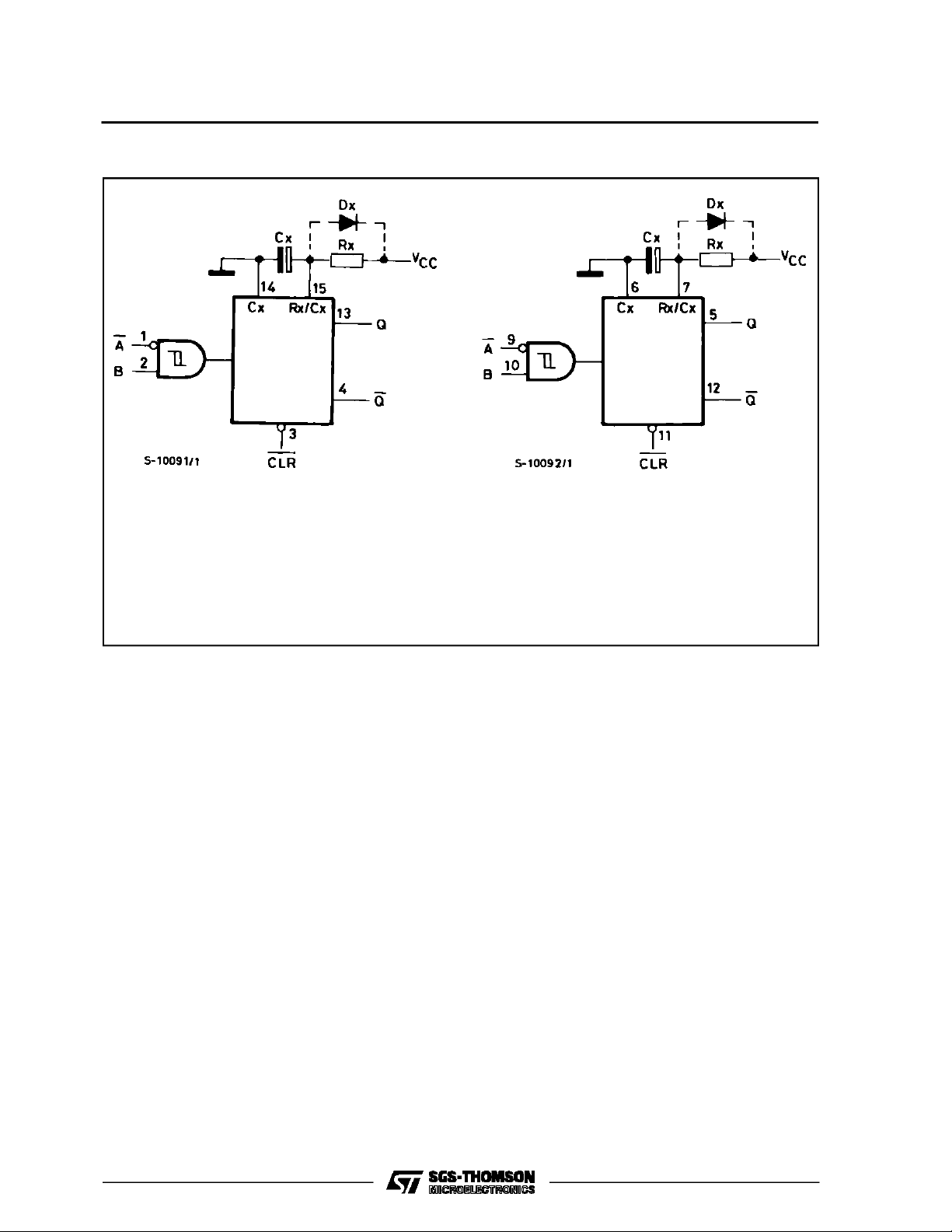
Limit forvalues of CxandRx :
Cx : NO LIMIT
Rx : VCC<3.0 V 5K Ω to 1 M Ω
VCC≥ 3.0 V 1 K Ω to 1 M Ω
Two different pulse width constants are available:
K ≅ 0.7 for HC221
K ≅ 1 for HC221A
All inputs are equipped with protection circuits
against static discharge and transient excess voltage.
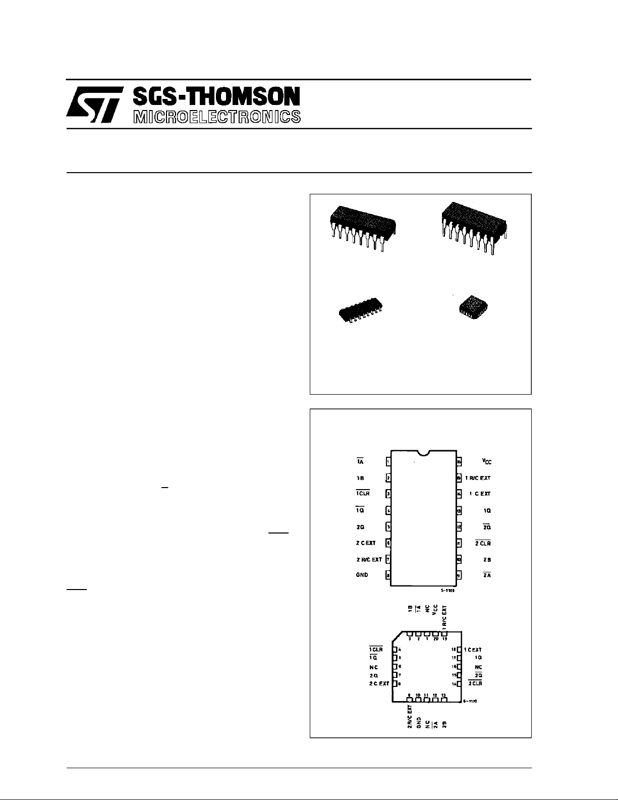
PIN CONNECTIONS(top view)
NC =
No Internal
Connection
October 1993
1/14
M54/M74HC221/221A
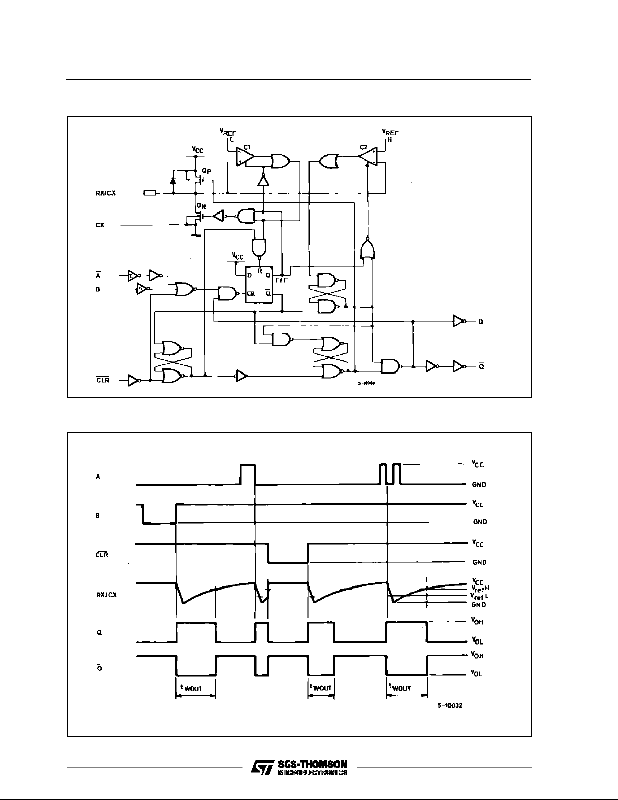
SYSTEM DIAGRAM
TIMING CHART
2/14
M54 / M74HC2 21 /221 A
BLOCK DIAGRAM
Note:
(1)Cx, Rx, Dx are externalcomponents.
(2)Dx isa clampingdiode.
Theexternalcapacitor ischarged toVCCinthestand-by state,i.e.notrigger.Whenthesupply voltageis turned offCxis dischargedmainly
throughan internalparasiticdiode (see figures). IfCx issufficientlylarge and VCCdecreases rapidy,therewill besomepossibility of damagingtheI.C.witha surgecurrentor latch-up. If the voltagesupply filtercapacitor is largeenough and VCCdecrease slowly,the surge
currentis automaticallylimitedand damage the I.C. is avoided. Themaximumforwardcurrentof the parasiticdiodeisapproximately 20
mA.In caseswhereCx is large the timetakenfor the supply voltageto fallto 0.4VCCcanbecalculated asfollows:
tf≥ (VCC–0.7)⋅Cx/20mA
Incases wheretfistoo short anexternal clampingdiode is required toprotect theI.C.fromthe surge current.
FUNCTIONAL DESCRIPTION
STAND-BYSTATE
The external capacitor, Cx, is fully charged to V
CC
inthe stand-bystate.Hence, beforetriggering,transistorQp andQn (connected tothe Rx/Cxnode)are
both turned-off. The two comparators that control
the timing and the two reference voltage sources
stop operating. The totalsupply current istherefore
only leakage current.
TRIGGEROPERATION
Triggering occurswhen :
1st) A is ”low” and B hasa falling edge;
2nd) B is”high” and Ahas a rising edge ;
3rd) A islowand Bis highand C1hasa risingedge.
After the multivibrator has been retriggered comparatorC1 and C2 start operating and Qn isturned
on. Cx then discharges through Qn.The voltageat
the node R/Cexternal falls.
Whenit reaches V
theoutputof comparatorC1
REFL
becomeslow. Thisin turnresetstheflip-flopandQn
is turnedoff.
At this pointC1 stopsfunctioning but C2 continues
to operate.
ThevoltageatR/Cexternalbeginstorisewithatime
constantset by the externalcomponents Rx, Cx.
Triggering themultivibratorcausesQto gohighafter
internal delay dueto the flip-flop and the gate. Qremains high until the voltage at R/C external rises
againto V
. AtthispointC2outputgoeslow and
REFH
O goes low. C2 stop operating. That means that
after triggering when the voltage R/C external returns to V
the multivibrator has returned to its
REFH
MONOSTABLESTATE. In the case whereRx ⋅ Cx
are large enough and thedischargetime of the capacitorand thedelaytime inthe I.C.can beignored,
the width ofthe output pulse tw (out) is as follows :
t
W(OUT)
= 0.70 Cx ⋅ Rx (HC221)
t
W(OUT)
=Cx⋅Rx (HC221A)
RESETOPERATION
CL isnormallyhigh.If CLislow,the triggeris not ef-
fectivebecauseQoutput goeslow and trigger control flip-flopis reset.
Also transistor Op is turned on and Cx is charged
quickyto VCC. Thismeans if CL inputgoes low,the
IC becomeswaiting state both inoperating andnon
operating state.
3/14
M54/M74HC221/221A
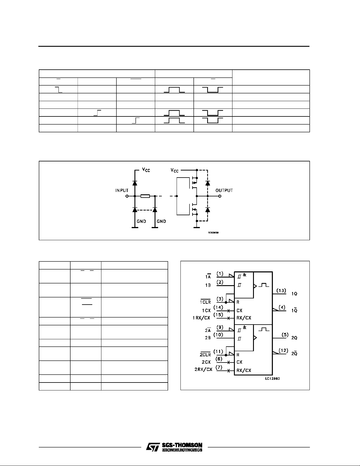
TRUTH TABLE
INPUTS OUTPUTS
A B CLR Q Q
H H OUTPUT ENABLE
X L H L (*) H (*) INHIBIT
H X H L (*) H (*) INHIBIT
L H OUTPUT ENABLE
L H OUTPUT ENABLE
X X L L H INHIBIT
X:Don’t Care (*):Except for monostble period
INPUT AND OUTPUT EQUIVALENT CIRCUIT
NOTE
PIN DESCRIPTION
PIN No SYMBOL NAME AND FUNCTION
1, 9 1A, 2A Trigger Inputs (Negative
Edge Triggered)
2, 10 1B, 2B Trigger Inputs (Positive
Edge Triggered)
3, 11 1CLR,
2CLR
4, 12 1Q, 2Q Outputs (Active LOW)
72R
EXT/CEXT
13, 5 1Q, 2Q Outputs (Active HIGH)
14, 6 1C
15 1R
EXT
2C
EXT
EXT/CEXT
8 GND Ground (0V)
16 V
CC
Direct Reset LOW and
Trigger Action at Positive
Edge
External Resistor
Capacitor Connection
External Capacitor
Connection
External Resistor
Capacitor Connection
Positive Supply Voltage
IEC LOGIC SYMBOL
4/14
M54 / M74HC2 21 /221 A
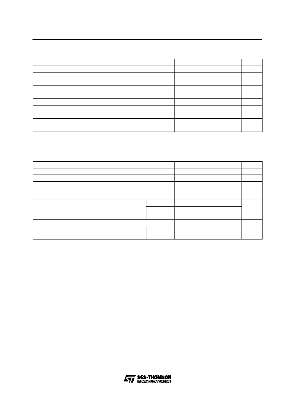
ABSOLU TE MAXIMU M RAT ING
Symbol Parameter Value Unit
V
CC
V
V
O
I
IK
I
OK
I
O
I
or I
CC
P
D
T
stg
T
AbsoluteMaximumRatingsarethosevalues beyondwhichdamagetothedevicemayoccur.Functionaloperationunderthesecondition isnotimplied.
(*)500 mW: ≅ 65oC derateto300mW by 10mW/oC: 65oCto85oC
RECO MM ENDED OPERATING C O NDITI O NS
Symbol Parameter Value Unit
V
CC
V
I
V
O
T
op
t
r,tf
C
X
R
X
(*)Themaximum allowablevaluesof Cx andRx are a functionof leackage ofcapacitor Cx,the leackage ofHC221/A, andleackage due to the
boardlayout and surfaceresistance. Susceptibility to externally inducednoise signals may occur for Rx> 1MΩ
Supply Voltage -0.5 to +7 V
DC Input Voltage -0.5 to VCC+ 0.5 V
I
DC Output Voltage -0.5 to VCC+ 0.5 V
DC Input Diode Current ± 20 mA
DC Output Diode Current ± 20 mA
DC Output Source Sink Current Per Output Pin ± 25 mA
DC VCCor Ground Current ± 50 mA
GND
Power Dissipation 500 (*) mW
Storage Temperature -65 to +150
Lead Temperature (10 sec) 300
L
Supply Voltage 2 to 6 V
Input Voltage 0 to V
Output Voltage 0 to V
Operating Temperature: M54HC Series
M74HC Series
CC
CC
-55 to +125
-40 to +85
Input Rise and Fall Time (CLR and A only) VCC= 2 V 0 to 1000 ns
V
= 4.5 V 0 to 500
CC
V
= 6 V 0 to 400
CC
External Capacitor > 100 (*) pF
External Resistor VCC<3V 5Kto1M(*) Ω
≥ 3 V 1K to 1M (*)
V
CC
o
C
o
C
V
V
o
C
o
C
5/14

M54/M74HC221/221A
DC SPECIFICATIO NS
Symbol Parameter
V
V
V
V
I
I
CC
(1):Per Circuit
High Level Input
IH
Voltage
Low Level Input
IL
Voltage
High Level
OH
Output Voltage
(Q, Q Output)
Low Level Output
OL
Voltage
(Q, Q Output)
I
Input Leakage
I
Current
R/C Terminal Off
I
I
State Current
Quiescent Supply
CC
Current
’ Active State
Supply Current (1)
Test Conditions Value
V
(V)
CC
=25oC
A
54HC and 74HC
Min. Typ. Max. Min. Max. Min. Max.
-40 to 85oC
74HC
-55 to 125oC
54HC
Unit
T
2.0 1.5 1.5 1.5
4.5 3.15 3.15 3.15
6.0 4.2 4.2 4.2
2.0 0.5 0.5 0.5
4.5 1.35 1.35 1.35
6.0 1.8 1.8 1.8
2.0
4.5 4.4 4.5 4.4 4.4
6.0 5.9 6.0 5.9 5.9
4.5 I
6.0 I
2.0
4.5 0.0 0.1 0.1 0.1
6.0 0.0 0.1 0.1 0.1
4.5 I
6.0 I
6.0
6.0
=
V
I
IO=-20 µA
V
IH
or
V
IL
=-4.0 mA 4.18 4.31 4.13 4.10
O
=-5.2 mA 5.68 5.8 5.63 5.60
O
V
=
I
IO=20µA
V
IH
or
V
IL
= 4.0 mA 0.17 0.26 0.33 0.40
O
= 5.2 mA 0.18 0.26 0.33 0.40
O
VI=VCCor GND ±0.1 ±1 ±1 µA
V
I=VCC
or GND ±0.5 ±5 ±10 µA
1.9 2.0 1.9 1.9
0.0 0.1 0.1 0.1
6.0 VI=VCCor GND 4 40 80 µA
2.0 VI=VCCor GND
4.5 400 530 650 850 µA
VIN=VCC/2
45 250 260 350 µA
6.0 0.7 1 1.3 1.7 mA
V
V
V
V
6/14

M54 / M74HC2 21 /221 A
AC ELECTRICAL CHARACTERISTICS (CL=50pF,Inputtr=tf=6ns)
Test Conditions Value
T
=25oC
Symbol Parameter
t
t
TLH
THL
Output Transition
Time
V
CC
(V)
2.0 30 75 95 110
4.5 8151922
A
54HC and 74HC
Min. Typ. Max. Min. Max. Min. Max.
6.0 7131619
t
PLH
t
PHL
t
PLH
t
PHL
t
PLH
t
PHL
t
WOUT
Propagation
Delay Time
(A, B - Q, Q)
Propagation
Delay Time
(CLRTRIGGER- Q,Q)
Propagation
Delay Time
(CLR - Q, Q)
Output Pulse
Width
(for HC221)
2.0 102 210 265 315
4.5 30 42 53 63
6.0 24 36 45 54
2.0 102 235 295 355
4.5 30 47 59 71
6.0 24 40 50 60
2.0 67 160 200 240
4.5 20 32 40 48
6.0 16 27 34 41
2.0 CX= 100 pF
R
=10KΩ
4.5 1.3
X
1.5
6.0 1.2
2.0 C
4.5 6.9
= 0.1 µF
X
RX= 100 KΩ
7
6.0 6.9
t
WOUT
Output Pulse
Width
(for HC221A)
2.0 CX= 100 pF
4.5 1.5
RX=10KΩ
1.8
6.0 1.4
2.0 C
4.5 9.7
= 0.1 µF
X
RX= 100 KΩ
10
6.0 9.6
∆t
WOUT
Output Pulse
±1
Width Error
Between Circuits
in Same Package
t
W(H)
t
W(L)
Minimum Pulse
Width
2.0 75 95 110
4.5 15 19 22
6.0 13 16 20
t
W(L)
Minimum Pulse
Width
2.0 75 95 110
4.5 15 19 22
6.0 13 16 20
C
C
PD
Input Capacitance 5 10 10 10 pF
IN
(*) Power Dissipation
174
Capacitance
(*) CPDisdefined as the valueofthe IC’s internal equivalent capacitance which is calculated from the operatingcurrent consumption withoutload.
(RefertoTestCircuit).Averageopertingcurrentcanbeobtainedbythefollowingequation.ICC(opr)=CPD•VCC•fIN+ICC’Duty/100+IC/2(permonostable)
(ICC’:ActiveSupply Current) (Duty:%)
-40 to 85oC
74HC
-55 to 125oC
54HC
Unit
ns
ns
ns
ns
µs
ms
µs
ms
%
ns
ns
pF
7/14

M54/M74HC221/221A
Output Pulse Width Constant Characteristics
(for HC221)
Output Pulse Width Characteristics (for HC221)
Output Pulse Width Constant Characteristics
(for HC221A)
Output Pulse Width Characteristics (for HC221A)
8/14

SWITCHING CHARACTERISTICS TEST WAVEFORM
M54 / M74HC2 21 /221 A
TEST WAVEFORM
Input TransitionTime : 6ns
VIH=VCC,VIL=GND.
9/14

M54/M74HC221/221A
Plastic DIP16 (0.25) MECHANICAL DATA
DIM.
MIN. TYP. MAX. MIN. TYP. MAX.
a1 0.51 0.020
B 0.77 1.65 0.030 0.065
b 0.5 0.020
b1 0.25 0.010
D 20 0.787
E 8.5 0.335
e 2.54 0.100
e3 17.78 0.700
F 7.1 0.280
I 5.1 0.201
L 3.3 0.130
Z 1.27 0.050
mm inch
10/14
P001C

Ceramic DIP16/1 MECHANICAL DATA
M54 / M74HC2 21 /221 A
DIM.
MIN. TYP. MAX. MIN. TYP. MAX.
A 20 0.787
B 7 0.276
D 3.3 0.130
E 0.38 0.015
e3 17.78 0.700
F 2.29 2.79 0.090 0.110
G 0.4 0.55 0.016 0.022
H 1.17 1.52 0.046 0.060
L 0.22 0.31 0.009 0.012
M 0.51 1.27 0.020 0.050
N 10.3 0.406
P 7.8 8.05 0.307 0.317
Q 5.08 0.200
mm inch
P053D
11/14

M54/M74HC221/221A
SO16 (Narrow) MECHANICAL DATA
DIM.
MIN. TYP. MAX. MIN. TYP. MAX.
A 1.75 0.068
a1 0.1 0.2 0.004 0.007
a2 1.65 0.064
b 0.35 0.46 0.013 0.018
b1 0.19 0.25 0.007 0.010
C 0.5 0.019
c1 45° (typ.)
D 9.8 10 0.385 0.393
E 5.8 6.2 0.228 0.244
e 1.27 0.050
e3 8.89 0.350
F 3.8 4.0 0.149 0.157
G 4.6 5.3 0.181 0.208
L 0.5 1.27 0.019 0.050
M 0.62 0.024
S8°(max.)
mm inch
12/14
P013H

PLCC20 MECHANICAL DATA
M54 / M74HC2 21 /221 A
DIM.
MIN. TYP. MAX. MIN. TYP. MAX.
A 9.78 10.03 0.385 0.395
B 8.89 9.04 0.350 0.356
D 4.2 4.57 0.165 0.180
d1 2.54 0.100
d2 0.56 0.022
E 7.37 8.38 0.290 0.330
e 1.27 0.050
e3 5.08 0.200
F 0.38 0.015
G 0.101 0.004
M 1.27 0.050
M1 1.14 0.045
mm inch
P027A
13/14

M54/M74HC221/221A
Information furnishedis believed to be accurate and reliable.However, SGS-THOMSON Microelectronics assumes no responsabilityfor the
consequences of useof such information norfor any infringementof patents or other rights of third parties which may results from its use. No
license is granted byimplication or otherwiseunder any patentor patent rightsof SGS-THOMSON Microelectronics.Specificationsmentioned
in thispublication are subjectto change without notice.This publication supersedes and replaces all information previouslysupplied.
SGS-THOMSON Microelectronicsproducts are not authorized foruse ascritical componentsin life supportdevices or systemswithout express
written approval ofSGS-THOMSON Microelectonics.
1994SGS-THOMSON Microelectronics- All Rights Reserved
Australia -Brazil - France- Germany- HongKong - Italy- Japan - Korea - Malaysia- Malta - Morocco -The Netherlands-
Singapore -Spain - Sweden - Switzerland -Taiwan -Thailand - United Kingdom -U.S.A
SGS-THOMSON Microelectronics GROUP OFCOMPANIES
14/14
 Loading...