

SGS Thomson Microelectronics M74HC195 Datasheet
.HIGH SPEED
tPD= 13 ns(TYP.) at VCC=5V
.LOWPOWERDISSIPATION
ICC=4µA(MAX.) at TA=25°C6V
.HIGH NOISEIMMUNITY
V
NIH=VNIL
=28%VCC(MIN.)
.OUTPUT DRIVE CAPABILITY
10 LSTTL LOADS
.SYMMETRICALOUTPUT IMPEDANCE
IOH =IOL= 4 mA(MIN.)
.BALANCEDPROPAGATION DELAYS
t
PLH=tPHL
.WIDE OPERATINGVOLTAGE RANGE
VCC(OPR)= 2 V to 6 V
.PIN ANDFUNCTION COMPATIBLE
WITH 54/74LS195
M54HC195
M74HC195
8 BITPIPO SHIFT REGISTER
B1R
(PlasticPackage)
M1R
(MicroPackage)
ORDER CODES :
M54HC 195F1R M74H C195M1R
M74HC 195B1R M74HC1 95C1R
F1R
(CeramicPackage)
C1R
(Chip Carrier)
DESCRIPTION
The M54/74HC195 is a high speed CMOS 4 BIT
PIPO SHIFT REGISTER fabricated in silicon gate
C2MOStechnology. Ithasthesamehighspeedperformance of LSTTL combined with true CMOS low
powerconsumption.
This shift register features parallel inputs, parallel
outputs, J-K serial inputs, a SHIFT/LOAD control
input,and a directoverridingCLEAR. Thisshift registercan operate intwo modes : Parallel Load ;Shift
from QAtowards QD.
Parallel loadingisaccomplishedbyapplying the four
bits of data, and taking the SHIFT/LOAD control
inputlow. The datais loaded intotheassociated flip
flops and appears at the outputs after the positive
transitionof the clockinput.During parallel loading,
serial data flow is inhibited. Serial shifting occurs
synchronously whenthe SHIFT/LOAD controlinput
ishigh.Serial data forthis mode isenteredattheJ-K
inputs. These inputs allowthe first stageto perform
as a J-Kor TOGGLE flip flopas shown inthe truthtable.
All inputs are equipped with protection circuits
against static discharge transient excess voltage.
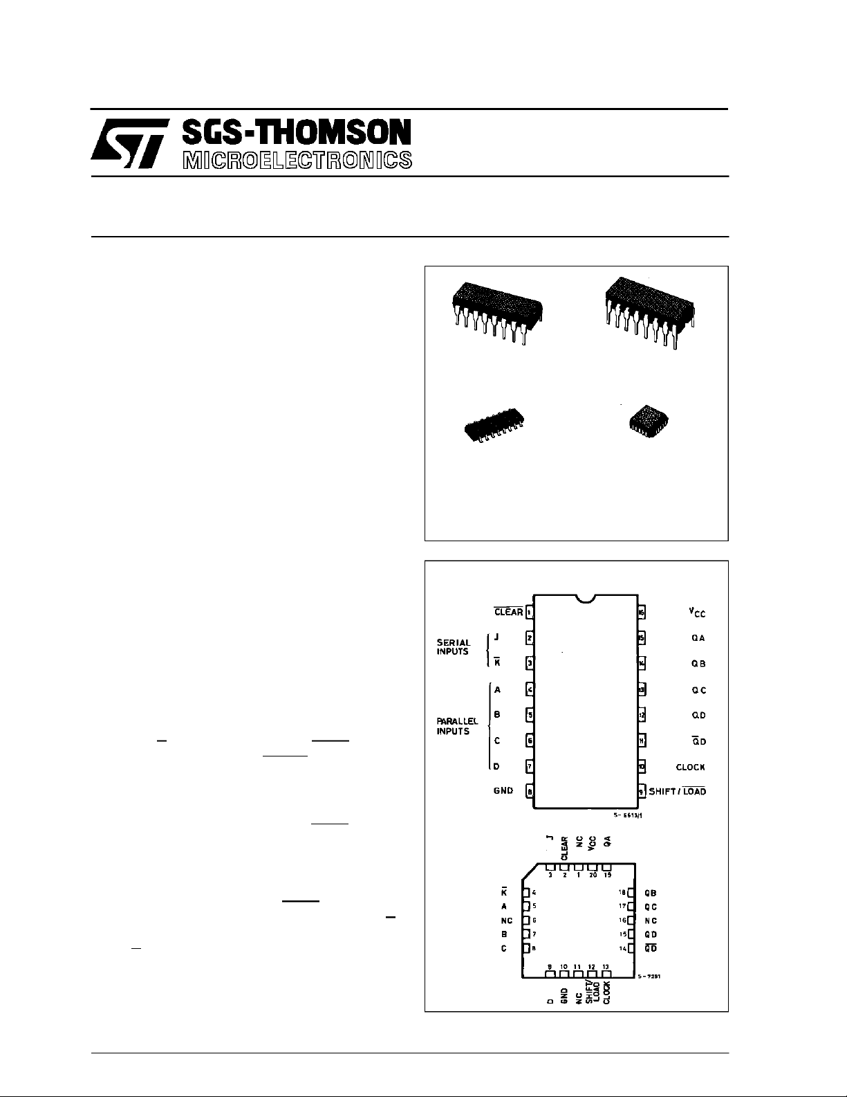
PIN CONNECTIONS(top view)
NC =
No Internal
Connection
October 1992
1/13
M54/M74HC195
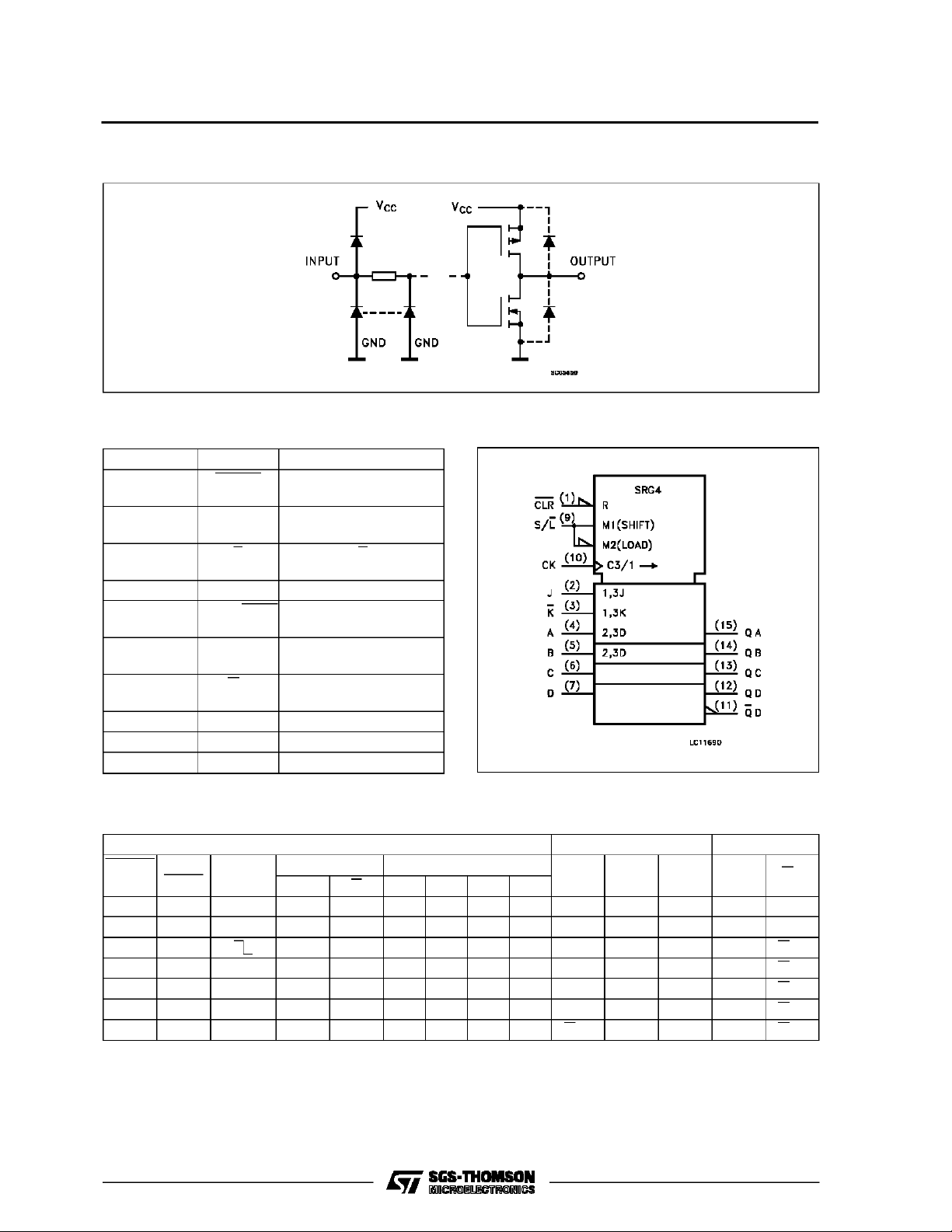
INPUT AND OUTPUT EQUIVALENT CIRCUIT
PIN DESCRIPTION
PIN No SYMBOL NAME AND FUNCTION
1 CLEAR Reset Input (Active
LOW)
2 J First Stage J Input
(Active LOW)
3 K First Stage K Input
(Active LOW)
4, 5, 6, 7 A to D Parallel Data Input
9 SHIFT/LOAD Control Input
10 CLOCK Clock Input (LOW to
HIGH Edge-triggered)
11 QD Inverted Output From
The Last Stage
15, 14, 13, 12 QA to QD Paralle Outputs
8 GND Ground (0V)
16 V
CC
Positive Supply Voltage
IEC LOGIC SYMBOL
TRUTH TABLE
INPUTS OUTPUS
CLEAR SHIFT/
LOAD
L X X X X XXXX L L L L L
HL XXabcdabcdd
H H X X XXXXQA0QB0QC0QD0QD0
H H L H XXXXQA0QA0QBnQCnQCn
H H L L XXXX L QAnQBnQCnQCn
H H H H XXXX HQAnQBnQCnQCn
H H H L XXXXQAnQAnQBnQCnQCn
X: Don’t Care: The level of QA,QB, QC, respectively, before the mst recent positivetransition of theclock.
CLOCK
SERIAL PARALLEL
J K ABCD
QA QB QC QD QD
2/13
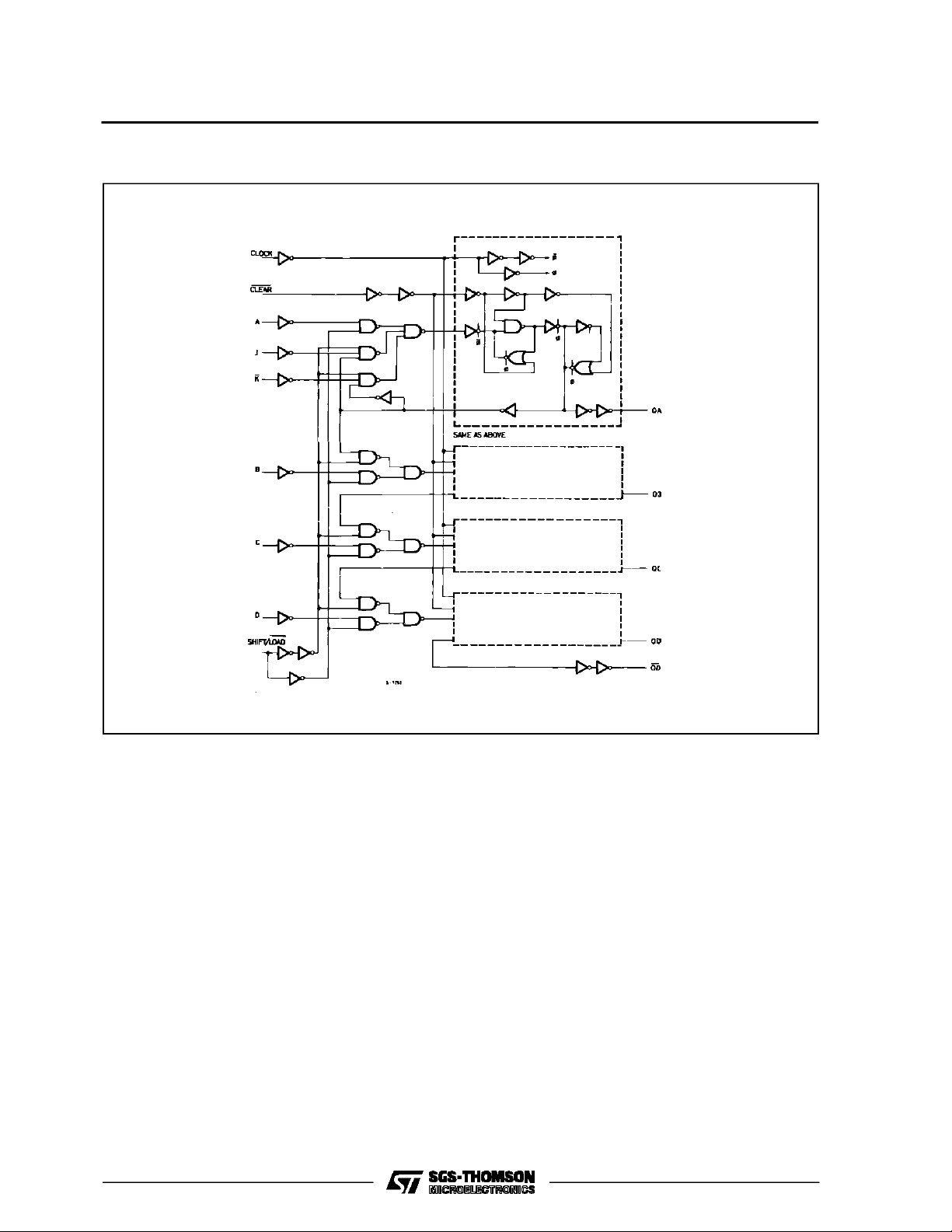
LOGIC DIAGRAM
M54/M74HC195
3/13
M54/M74HC195
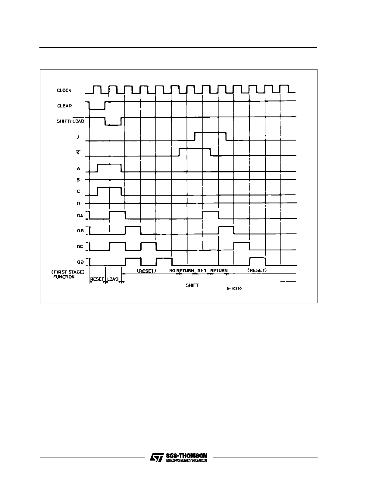
TIMING CHART
4/13
 Loading...