

SGS Thomson Microelectronics M74HC193, M74HC192 Datasheet
HC192 - SYNCHRONOUS UP/DOWN DECADE COUNTER
HC193 - SYNCHRONOUS UP/DOWN BINARY COUNTER
.HIGH SPEED
f
= 54 MHz(TYP.) AT VCC=5V
MAX
.LOWPOWERDISSIPATION
ICC=4µA(MAX.) AT TA=25°C
.HIGH NOISEIMMUNITY
V
NIH=VNIL
=28%VCC(MIN.)
.OUTPUT DRIVE CAPABILITY
10 LSTTL LOADS
.SYMMETRICALOUTPUT IMPEDANCE
|IOH|=IOL=4 mA(MIN.)
.BALANCEDPROPAGATION DELAYS
t
PLH=tPHL
.WIDE OPERATINGVOLTAGERANGE
VCC(OPR)= 2 V TO6 V
.PIN AND FUNCTION COMPATIBLE WITH
54/74LS192-193
DESCRIPTION
The M54/74HC192/193 are ahigh speed CMOSSYNCHRONOUS UP/DOWNDECADE COUNTERS fabricatedinsilicon gate C2MOStechnology. They have
thesamehigh speedperformance ofLSTTLcombined
with true CMOS low power consumption. The counter
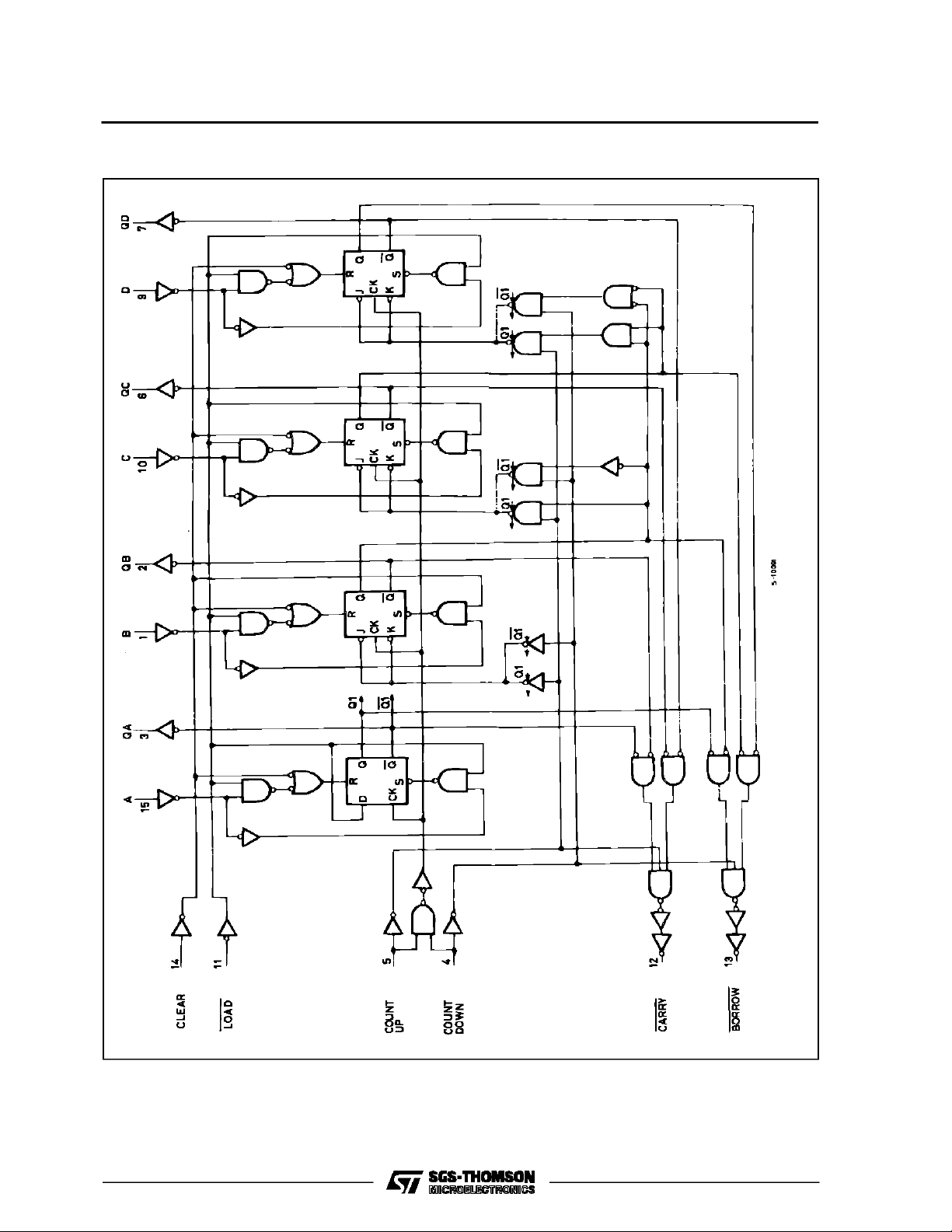
has two separate clock inputs, an UP COUNT input
and a DOWN COUNT input. All outputs of the flip-flop
are simultaneously triggered on the low to high transitionof either clock while theother inputisheldh igh. The
direction of counting is determined by which input is
clocked. This counter may be preset by entering the
desired dataon the DATAA, DATAB, DATA C, and
DATA D input.Whenthe LOADinput istaken lowthe
data is loaded independently of either clock input. This
featureallows the counters to be used asdivide-by-n
counters by modifying the count length with the preset
inputs. Inaddition thecountercanalso becleared. This
is accomplished by inputting a high on the CLEAR
input. All 4 in ternal stages are set to lowindependently
of ei ther COUNTinput. BothaB ORROWa ndCARRY
output areprovided toenablecascadingofbothupand
down counting functions. The BORROWoutput producesa negativegoingpulsewhen thecounterunderflows and the CARRY outputs a pulse when the
counter overflows. The counter can be cascaded by
connecting the CARRY and BORROW outputs of one
device to the COUNT UP and COUNTDOWN inputs,
respectively, of thenext device. Allinputs areequipped
with protection circuits against static discharge and
transient excess voltage.
M54/M74HC192
M54/M74HC193
B1R
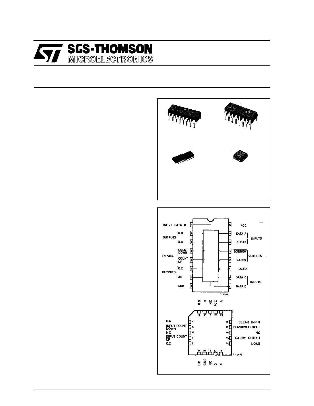
(PlasticPackage)
M1R
(MicroPackage)
M54HC X XXF1R M74H CXXXM1R
M74HC X XXB1R M74HCX X XC1R
NC =
No Internal
Connection
ORDER CODES :
PIN CONNECTIONS(top view)
F1R
(CeramicPackage)
C1R
(Chip Carrier)
October 1992
1/15
M54/M74HC192/193
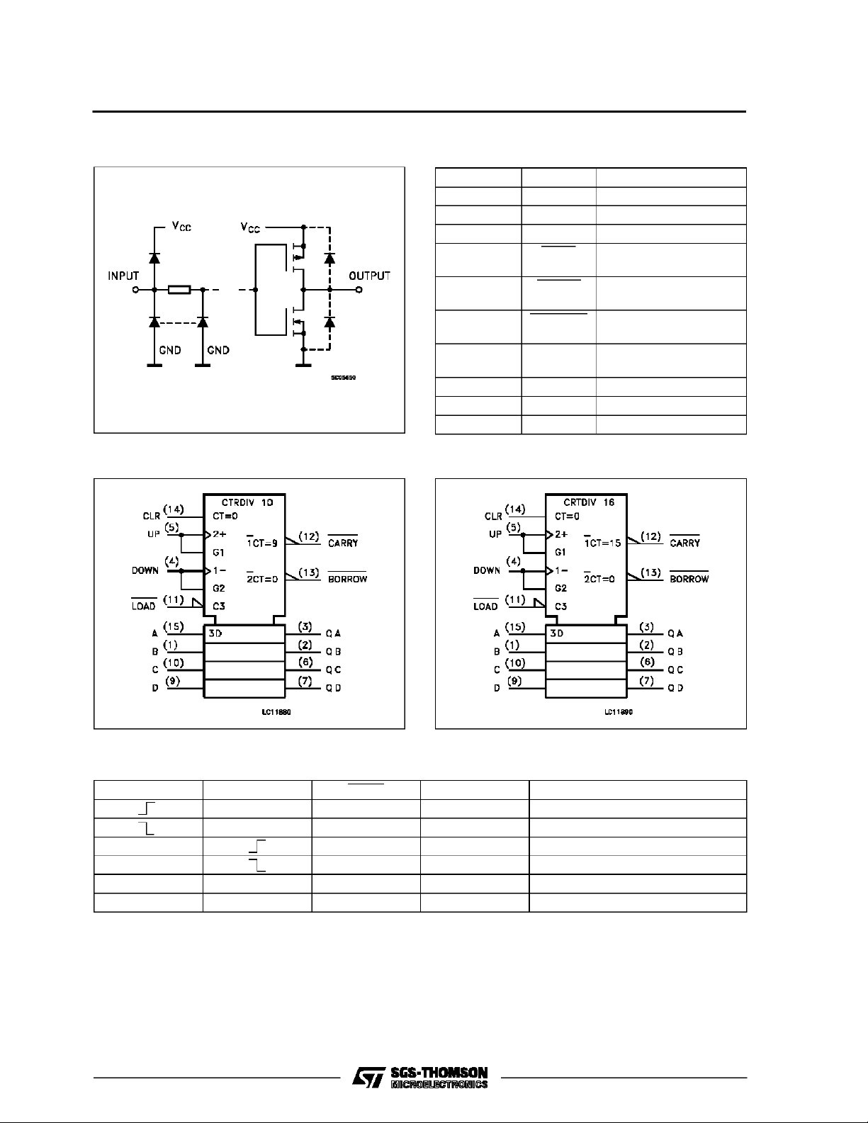
INPUT AND OUTPUT EQUIVALENT CIRCUIT
PIN DESCRIPTI ON
PIN No SYMBOL NAME AND FUNCTION
3, 2, 6, 7 QA to QD Flip-Flop Outputs
4CP
5CP
Count Down Clock Input
D
Count Up Clock Input
U
11 LOAD AsynchronousParallel
Load Input (Active LOW)
12 CARRY Count Up (Carry)
Output (Active LOW)
13 BORROW Count Down (Borrow)
Output (Active LOW)
14 CLEAR Asynchronous Reset
Input (Active HIGH)
15, 1, 10, 9 DA to DD Data Inputs
8 GND Ground (0V)
16 V
CC
Positive Supply Voltage
IEC LOGIC SYMBOL (HC193)IEC LOGIC SYMBOL (HC191)
TRUTH TABLE
COUNT UP COUNT DOWN LOAD CLEAR FUNCTION
H H L COUNT UP
H H L NO COUNT
H H L COUNT DOWN
H H L NO COUNT
X X L L PRESET
X X X H RESET
X: Don’t Care
2/15
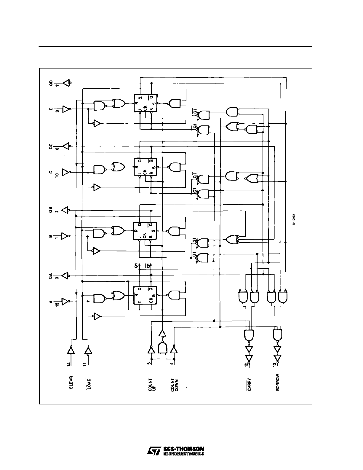
LOGIC DIAGAM (HC192)
M54/M74HC192/193
3/15
M54/M74HC192/193
LOGIC DIAGAM (HC193)
4/15
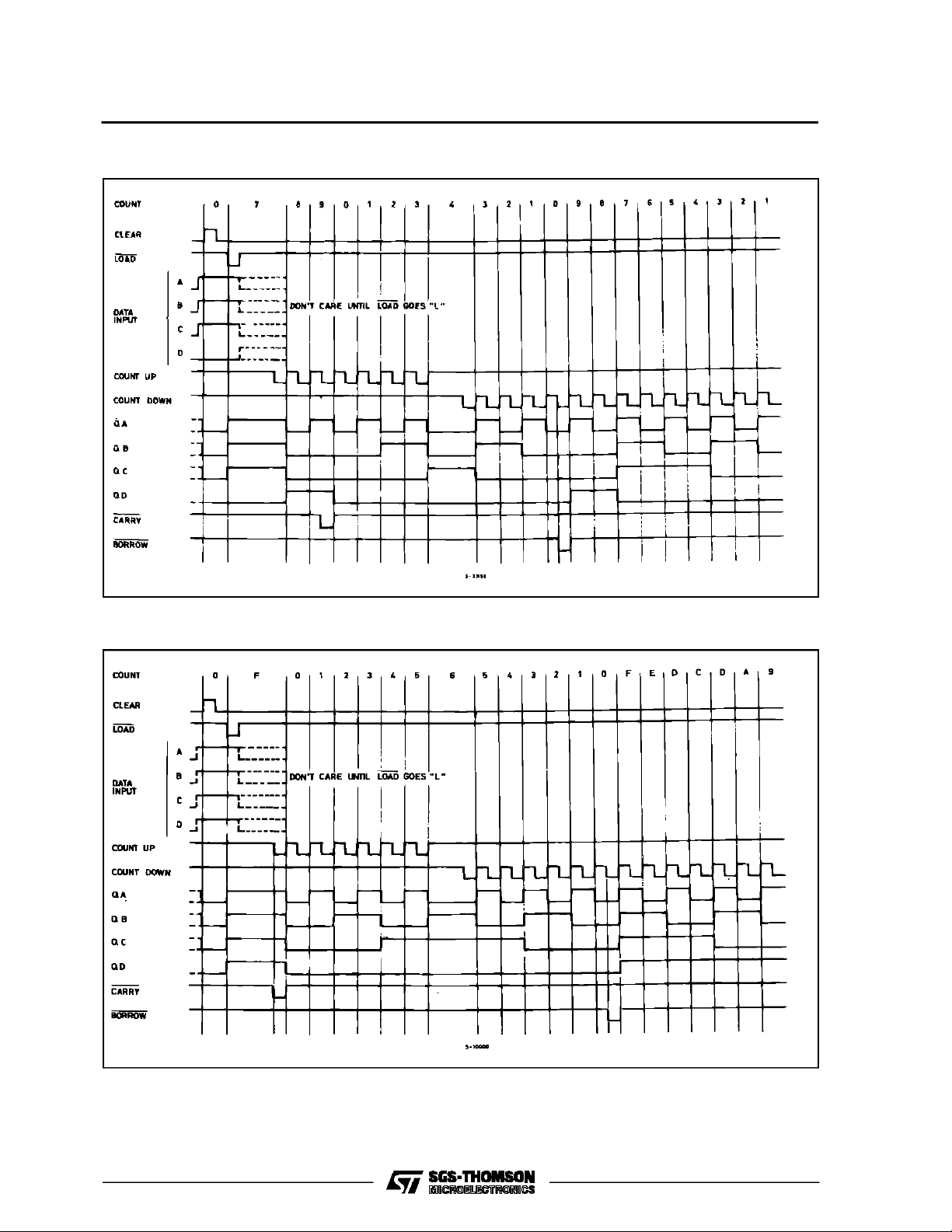
TIMING DIAGRAM (HC192)
M54/M74HC192/193
TIMING DIAGRAM (HC193)
5/15
 Loading...