

4 BIT SYNCHRONOUS UP/DOWN COUNTERS
.HIGH SPEED
f
= 48 MHz(TYP.) AT VCC=5V
MAX
.LOWPOWERDISSIPATION
ICC=4µA(MAX.) AT TA=25 °C
.HIGH NOISEIMMUNITY
V
NIH=VNIL
=28%VCC(MIN.)
.OUTPUT DRIVE CAPABILITY
10 LSTTL LOADS
.SYMMETRICALOUTPUT IMPEDANCE
IOH =IOL= 4 mA(MIN.)
.BALANCEDPROPAGATION DELAYS
t
PLH=tPHL
.WIDE OPERATINGVOLTAGERANGE
VCC(OPR)= 2V TO 6 V
.PIN AND FUNCTION COMPATIBLE
WITH 54/74LS190/191
M54/M74HC190
M54/M74HC191
B1R
(PlasticPackage)
M1R
(MicroPackage)
ORDER CODES :
M54HC X XXF1R M74H CXXXM1R
M74HC X XXB1R M74HCX X XC1R
F1R
(CeramicPackage)
C1R
(Chip Carrier)
DESCRIPTION
TheM54/74HC190/191 are highspeedCMOS4-BIT
SYNCHRONOUS UP/DOWN COUNTERS fabricatedinsilicon gateC2MOStechnology.
They have the same high speed performance of
LSTTL combined with true CMOS low power consumption.
State changes of the counter are synchronous with
theLOW-to-HIGHtransition ofthe Clock Pulse input.
Anasynchronous parallel load input overrides counting and loadsthe data present ontheDATA inputs into
the flip-flops, which makes it possible to use the circuitsasprogrammable counters. Acountenable input
serves as the carry/borrow input in multi-stage
counters. Control input, Down/Up, determines
whether acircuitcounts up ordown.A MAX/MINoutputandaRippleClockoutputprovideoverflow/underflow indication and make possible a variety of
methods forgenerating carry/borrow signalsin multistagecounter applications.
Allinputs areequipped withprotectioncircuitsagainst
staticdischarge and transient excess voltage.
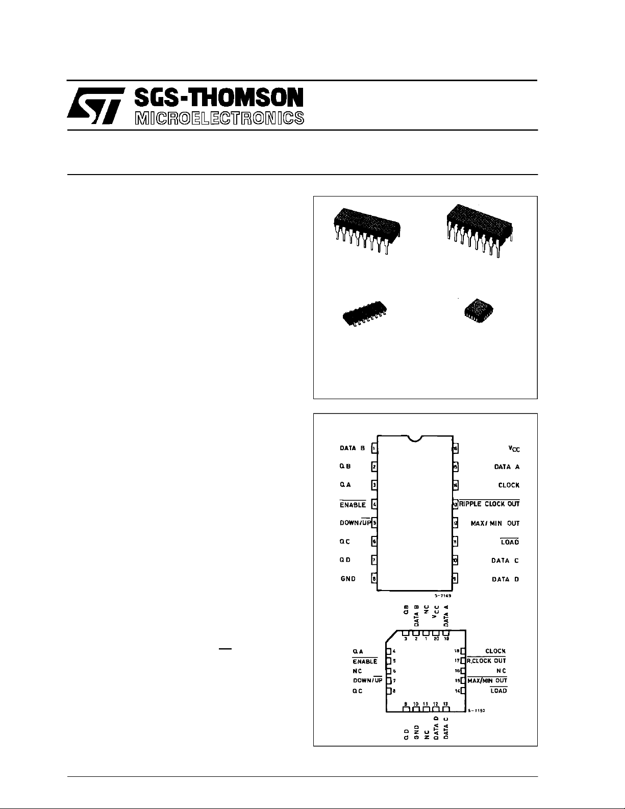
NC =
No Internal
Connection
PIN CONNECTIONS(top view)
October 1992
1/14
M54/M74HC190/191
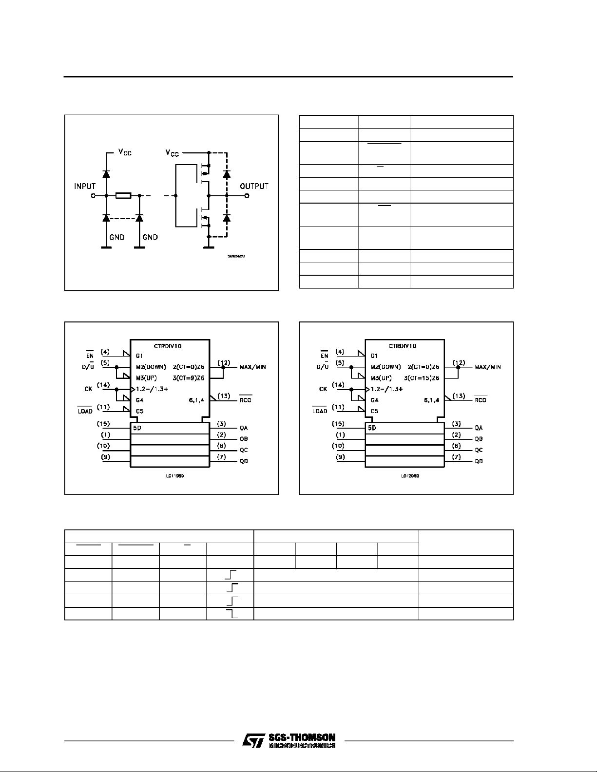
INPUT AND OUTPUT EQUIVALENT CIRCUIT
PIN DESCRIPTIO N
PIN No SYMBOL NAME AND FUNCTION
3, 2, 6, 7 QA to QD Flip-Flop Outputs
4 ENABLE Count Enable Input
(Active LOW)
5 U/D Parallel Data Input
11 LOAD Load Input (Active LOW)
12 MA/MI OUT Terminal Count Output
13 RC Ripple Clock Output
(Active LOW)
14 CLOCK Cloack Input (LOW to
HIGH, Edge-triggered)
15, 1, 10, 9 DA to DD Data Inputs
8 GND Ground (0V)
16 V
CC
Positive Supply Voltage
IEC LOGIC SYMBOL (HC191)IEC LOGIC SYMBOL (HC190)
TRUTH TABLE
INPUTS OUTPUS
LOAD ENABLE D/U CLOCK QA QB QC QD
L X X X a b c d PRESET DATA
H L L UP COUNT UP COUNT
H L H DOWN COUNT DOWN COUNT
H H X NO CHANGE NO COUNT
H X X NO CHANGE NO COUNT
X: Don’t Care
a -d: Thelevel of steadystate inputs atinputs a through Drespectively
2/14
FUNCTION
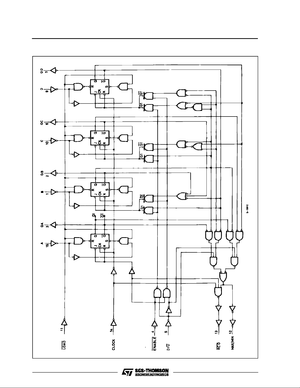
LOGIC DIAGRAM (HC190)
M54/M74HC190/191
3/14
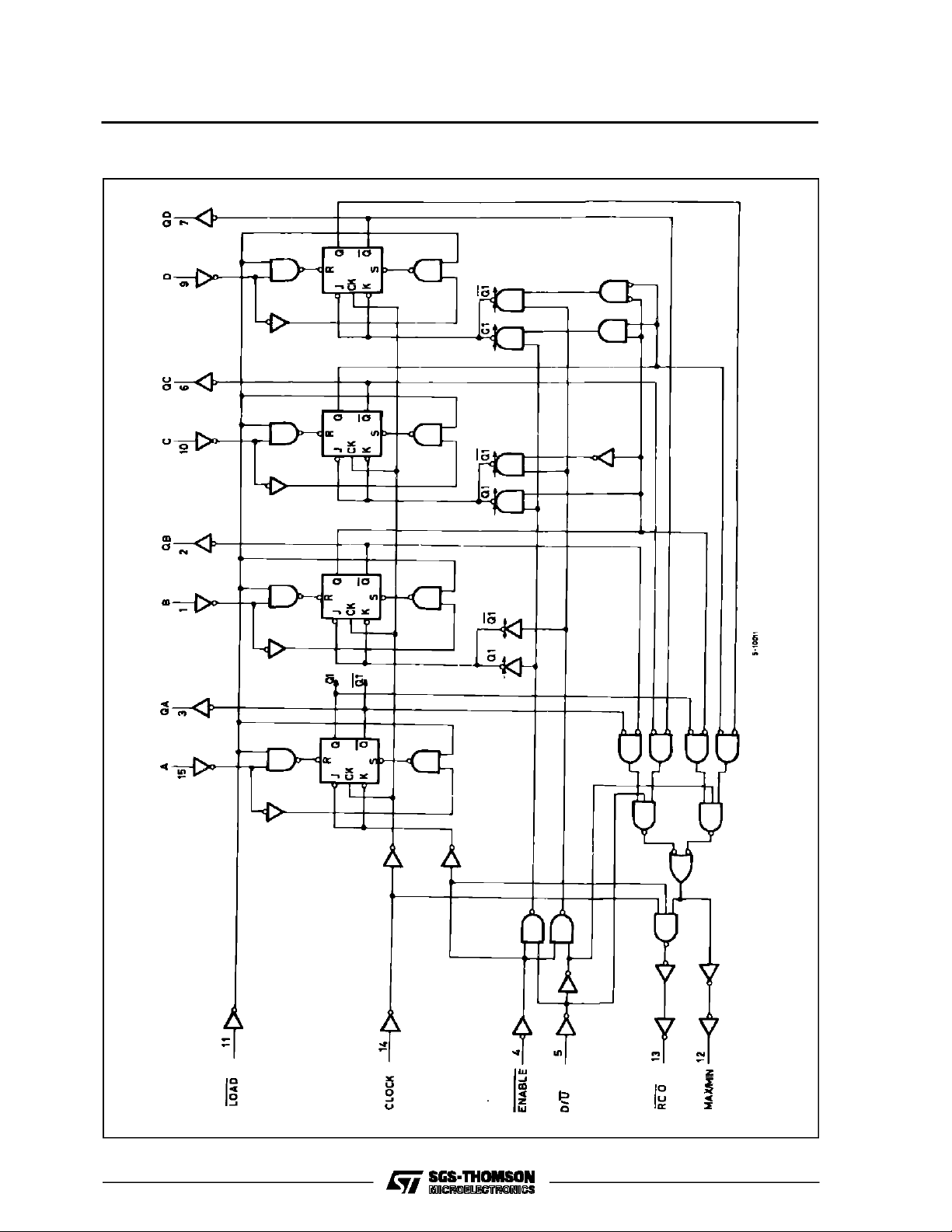
M54/M74HC190/191
LOGIC DIAGRAM (HC191)
4/14
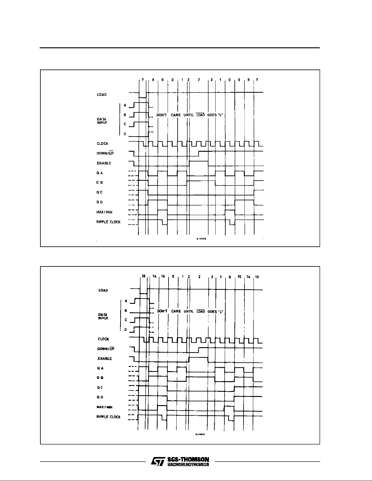
TIMING CHART (HC190)
M54/M74HC190/191
TIMING CHART (HC191)
5/14
 Loading...