

.HIGH SPEED
f
= 57 MHz(TYP.) AT VCC=5V
MAX
.LOWPOWERDISSIPATION
ICC=4µA(MAX.) AT TA=25°C
.HIGH NOISEIMMUNITY
V
NIH=VNIL
=28%VCC(MIN.)
.OUTPUT DRIVE CAPABILITY
10 LSTTL LOADS
.SYMMETRICALOUTPUT IMPEDANCE
|IOH|=IOL=4 mA(MIN.)
.BALANCEDPROPAGATION DELAYS
t
PLH=tPHL
.WIDE OPERATINGVOLTAGE RANGE
VCC(OPR)= 2 V TO6 V
.PIN AND FUNCTION COMPATIBLE WITH
54/74LS166
M54HC166
M74HC166
8 BITPISO SHIFT REGISTER
B1R
(PlasticPackage)
M1R
(MicroPackage)
ORDER CODES :
M54HC 166F1R M74H C166M1R
M74HC 166B1R M74HC1 66C1R
F1R
(CeramicPackage)
C1R
(Chip Carrier)
DESCRIPTION
The M54/74HC166 is a high speed C2MOS 8 BIT
PISO SHIFT REGISTER fabricated in silicon gate
C2MOStechnology. Ithasthesamehighspeedperformance of LSTTL combined with true CMOS low
powerconsumption.
It consists of parallel or serial inputsand aserial-out
8-bit shift register with gated clock inputs and an
overriding clear input. The parallel-in or serial-in
modes are controlled by the SHIFT/LOAD input.
Whenthe SHIFT/LOADinputis held high, theserial
data input isenabled andtheeightflip-flopsperform
serialshiftingwitheach clockpulse.When heldlow,
the parallel data inputs are enabled and synchronous loading occurs on the next clock pulse.
Clocking is accomplished on the low-to-high level
edge of theclock pulse. The CLOCK-INHIBITinput
should be changed to the high only while the
CLOCKinput is held high. A directclear input overrides all other inputs, including the clock, and sets
all flip-flops to zero. Functional detailsareshown in
the truthtable and the timing chart.
All inputs are equipped with protection circuits
against static discharge and transient excess voltage.
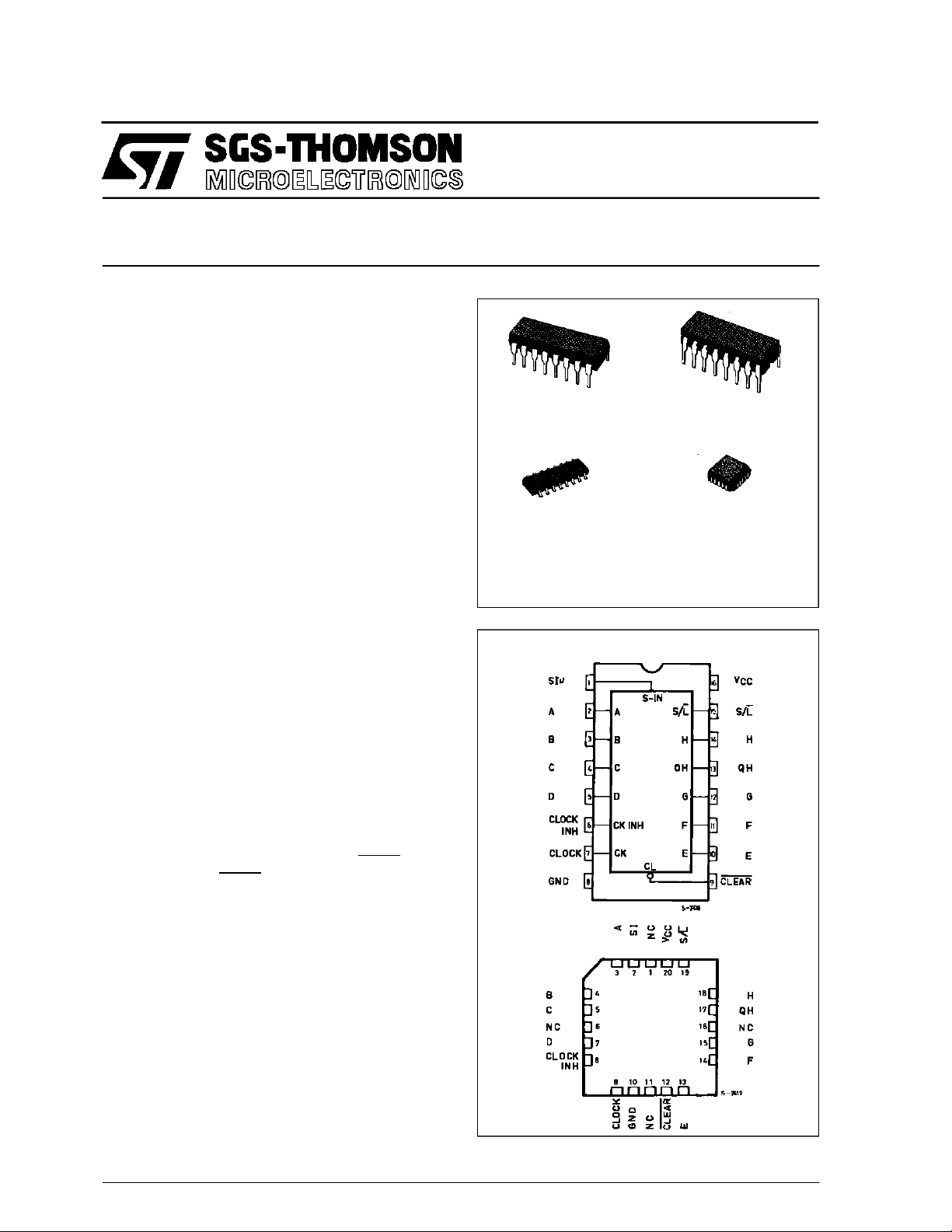
PIN CONNECTIONS(top view)
NC =
No InternalCon-
October 1992
1/13
M54/M74HC166
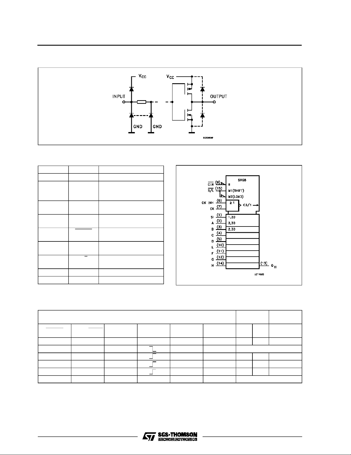
INPUT AND OUTPUT EQUIVALENT CIRCUIT
PIN DESCRIPTION
IEC LOGIC SYMBOL
PIN No SYMBOL NAME AND FUNCTION
1 SI Serial Data Inputs
2, 3, 4, 5,
A to H Parallel Data Inputs
10, 11, 12,
14
6 CK INH Clock Enable Input
(Active LOW)
7 CK Clock Input (LOW to
HIGH edge-triggered)
9 CLEAR Asyncronous Master reset
Input (Active LOW)
13 Q
H
Serial Output from the
Last Stage
15 S/L ParallelEnable Input
(Active LOW)
8 GND Ground (0V)
16 V
CC
Positive Supply Voltage
TRUTH TABLE
INPUTS
CLEAR SHIFT/LOAD CLOCK INH CLOCK SERIAL IN
PARALLEL
...............
A
LXXXXXLLL
L X X X X NO CHANGE
HLL Xa
................
H H L H X H QAn QGn
H H L L X L QAn QGn
H X H X X X NO CHANGE
X:Don’tCare
...........
a
h : Thelevel ofsteady stateinput voltageat inputs a trough H respectively
INTERNAL
OUTPUTS
QA QB QH
H
OUTPUTS
ha b h
2/13
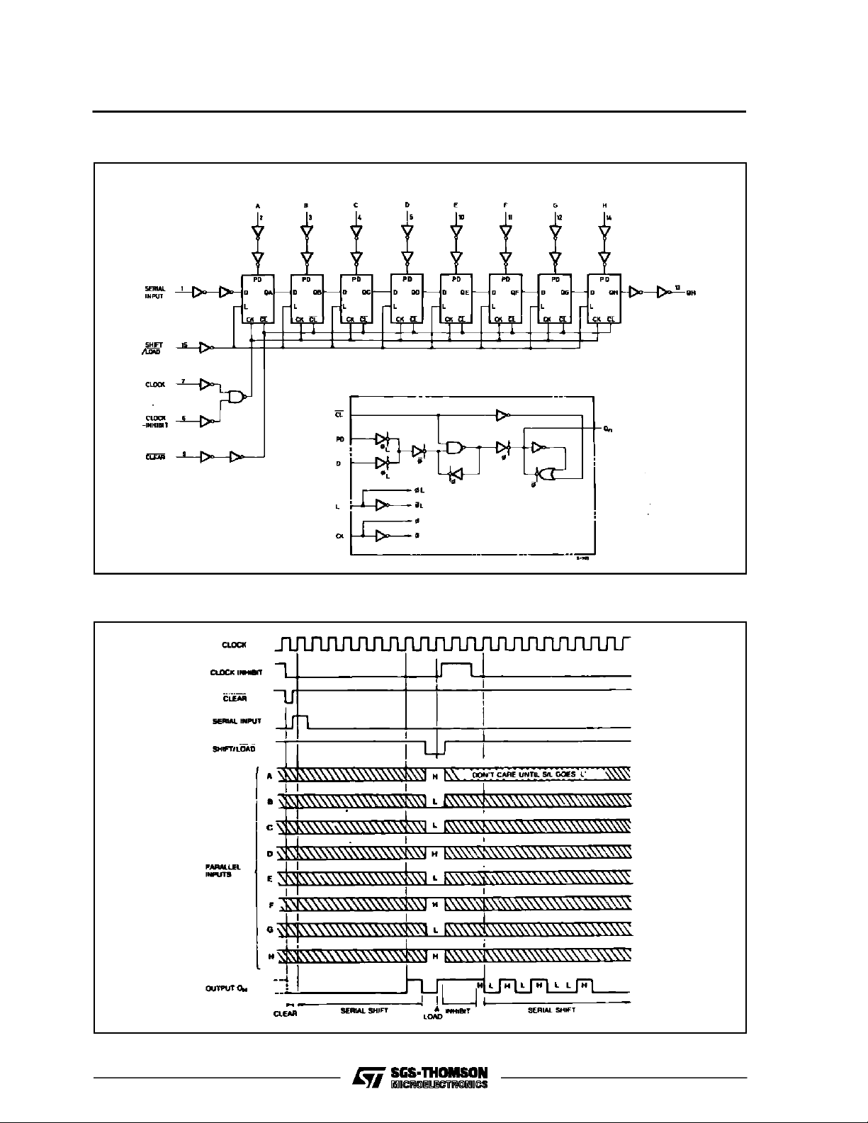
LOGIC DIAGRAM
M54/M74HC166
PARALLEL INPUTS
TIMING CHART
3/13
M54/M74HC166
ABSOLU TE MAXIMU M RATINGS
Symbol Parameter Value Unit
V
CC
V
V
O
I
IK
I
OK
I
O
I
or I
CC
P
D
T
stg
T
AbsoluteMaximumRatingsarethose values beyondwhichdamage tothedevicemayoccur. Functionaloperationunder these conditionisnotimplied.
(*)500 mW: ≅ 65oC derateto300mWby 10mW/oC: 65oCto85oC
RECO MM ENDED O PERAT IN G C O NDITI O NS
Symbol Parameter Value Unit
V
CC
V
I
V
O
T
op
t
r,tf
Supply Voltage -0.5 to +7 V
DC Input Voltage -0.5 to VCC+ 0.5 V
I
DC Output Voltage -0.5 to VCC+ 0.5 V
DC Input Diode Current ± 20 mA
DC Output Diode Current ± 20 mA
DC Output Source Sink Current Per Output Pin ± 25 mA
DC VCCor Ground Current ± 50 mA
GND
Power Dissipation 500 (*) mW
Storage Temperature -65 to +150
Lead Temperature (10 sec) 300
L
Supply Voltage 2 to 6 V
Input Voltage 0 to V
Output Voltage 0 to V
Operating Temperature: M54HC Series
M74HC Series
CC
CC
-55 to +125
-40 to +85
Input Rise and Fall Time VCC= 2 V 0 to 1000 ns
V
= 4.5 V 0 to 500
CC
V
= 6 V 0 to 400
CC
o
C
o
C
V
V
o
C
o
C
4/13
 Loading...