

SGS Thomson Microelectronics M74HC165 Datasheet
.HIGH SPEED
tPD= 15 ns(TYP.) AT VCC=5V
.LOWPOWERDISSIPATION
ICC=4µA(MAX.) AT TA=25°C
.OUTPUTDRIVE CAPABILITY
10 LSTTL LOADS
.BALANCEDPROPAGATION DELAYS
t
PLH=tPHL
.SYMMETRICALOUTPUT IMPEDANCE
IOL=IOH = 4 mA (MIN.)
.HIGH NOISE IMMUNITY
V
NIH=VNIL
=28%VCC(MIN.)
.WIDE OPERATINGVOLTAGE RANGE
VCC(OPR)= 2 V TO6 V
.PIN ANDFUNCTION COMPATIBLE
WITH 54/74LS165
M54HC165
M74HC165
8 BITPISO SHIFT REGISTER
B1R
(PlasticPackage)
M1R
(MicroPackage)
ORDER CODES :
M54HC 165F1R M74H C165M1R
M74HC 165B1R M74HC1 65C1R
F1R
(CeramicPackage)
C1R
(Chip Carrier)
DESCRIPTION
The M54/74HC165 is a high speed CMOS 8 BIT
PISO SHIFT REGISTER fabricated in silicon gate
C2MOS technology. It has the same high speed
performance of LSTTL combined with true CMOS
low powerconsumption.
It achives the high speed operation similar to
equivalent LSTTL whilemaintaining the CMOSlow
powerdissipation.
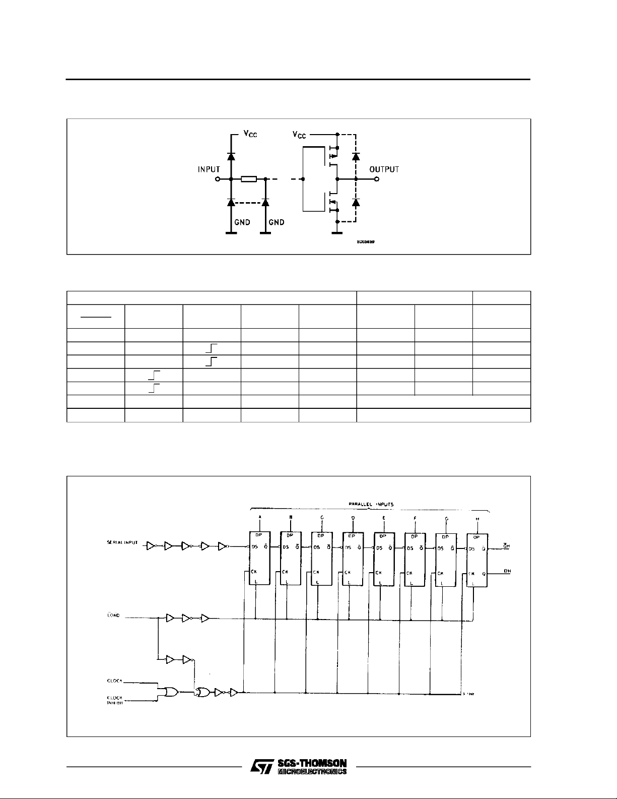
Thisdevice contains eight clockedmasterslave RS
flip-flopsconnected as a shift register, with auxiliary
gating to provide over-riding asynchronous parallel
entry.Parallel data entres whenthe shift/load input
is low.The parallel datacan change while shift/load
is low, provided that the recommended set-upand
hold times are observed. For clocked operation,
shift/loadmustbe high. The twoclock input perform
identically; one can be used as a clock inhibit by
applying a high signal; to permit this operation
clockingisaccomplished through a2inputnorgate.
Toavoiddoubleclocking,however, the inhibit signal
should only go high while the clock is high.
Otherwise the rising inhibit signal will cause the
same response as rising clock edge.
All inputs are equipped with protection circuits
against static discharge and transient excess
voltage.
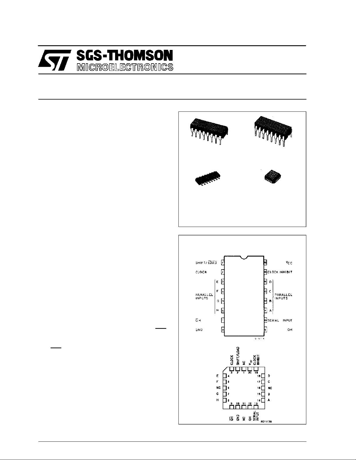
PIN CONNECTIONS(top view)
NC =
No Internal
Connection
September 1993
1/13
M54/M74HC165
INPUT AND OUTPUT EQUIVALENT CIRCUIT
TRUTH TABLE
INPUTS INTERNAL OUTPUTS OUTPUS
SHIFT/
CLEAR
L X X X a............h a b h
H L H X H QAn QGn
H L L X L QAn QGn
H L H X H QAn QGn
H L L X L QAn QGn
H X H X X NO CHANGE
H H X X X NO CHANGE
a.......h:The level of steadyinput voltage atinputs athroughrespectively
QAn- QGn : The levelof QA -QG,respectively. beforethemost-recent transitionof theclock.
CLOCK
INHIBIT
CLOCK SERIAL IN A .........H QA QB QH
LOGI C DIAG RAM
2/13
M54/M74HC165
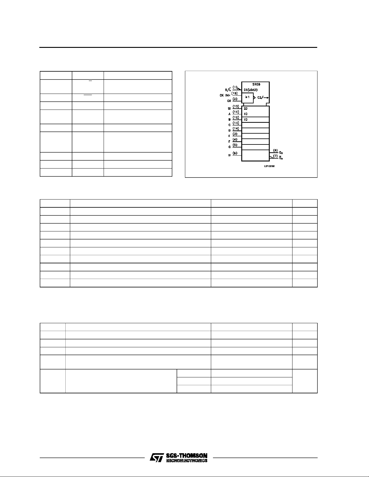
PIN DESCRIPTIO N
IEC LOGIC SYMBOL
PIN No SYMBOL NAME AND FUNCTION
1 S/L Asynchronous Parallel
Load Input
2 QH Complementary Output
7 QH Serial Output
9 CLOCK Clock Input (LOW to
HIGH edge triggered)
10 SI Serial Data Input
11, 12, 13,
A to H Parallel Data Inputs
14, 3, 4, 5,
6
15 CLOCK INH CLock Inhibit
8 GND Ground (0V)
16 V
CC
Positive Supply Voltage
ABSOLU TE MAXIMU M RATINGS
Symbol Parameter Value Unit
V
CC
V
V
O
I
IK
I
OK
I
O
or I
I
CC
P
D
T
stg
T
L
AbsoluteMaximumRatingsarethosevaluesbeyondwhichdamage tothedevice mayoccur. Functionaloperationunder theseconditionisnotimplied.
(*)500 mW:≅ 65oC derateto 300 mW by 10mW/oC: 65oCto85oC
Supply Voltage -0.5 to +7 V
DC Input Voltage -0.5 to VCC+ 0.5 V
I
DC Output Voltage -0.5 to VCC+ 0.5 V
DC Input Diode Current ± 20 mA
DC Output Diode Current ± 20 mA
DC Output Source Sink Current Per Output Pin ± 25 mA
DC VCCor Ground Current ± 50 mA
GND
Power Dissipation 500 (*) mW
Storage Temperature -65 to +150
Lead Temperature (10 sec) 300
o
C
o
C
RECO MM ENDED O PERAT IN G C O NDITI O NS
Symbol Parameter Value Unit
V
V
T
t
V
r,tf
Supply Voltage 2 to 6 V
CC
Input Voltage 0 to V
I
Output Voltage 0 to V
O
Operating Temperature: M54HC Series
op
M74HC Series
CC
CC
-55 to +125
-40 to +85
Input Rise and Fall Time VCC= 2 V 0 to 1000 ns
V
= 4.5 V 0 to 500
CC
= 6 V 0 to 400
V
CC
V
V
o
C
o
C
3/13
M54/M74HC165
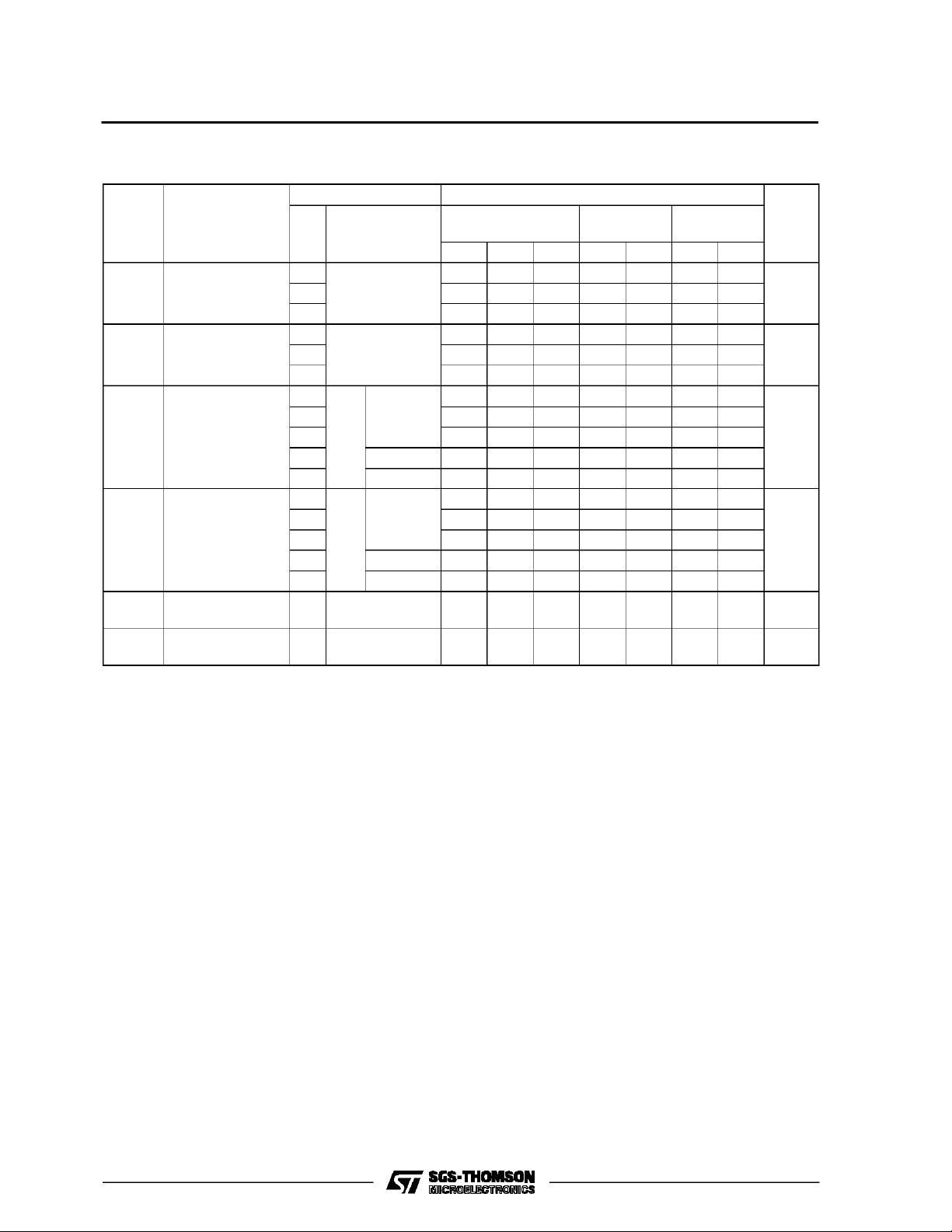
DC SPECIFICATIO NS
Symbol Parameter
V
V
V
V
I
High Level Input
IH
Voltage
Low Level Input
IL
Voltage
High Level
OH
Output Voltage
Low Level Output
OL
Voltage
I
Input Leakage
I
Current
Quiescent Supply
CC
Current
Test Conditions Value
V
(V)
CC
=25oC
A
54HC and 74HC
Min. Typ. Max. Min. Max. Min. Max.
-40 to 85oC
74HC
-55 to 125oC
54HC
Unit
T
2.0 1.5 1.5 1.5
4.5 3.15 3.15 3.15
6.0 4.2 4.2 4.2
2.0 0.5 0.5 0.5
4.5 1.35 1.35 1.35
6.0 1.8 1.8 1.8
2.0
4.5 4.4 4.5 4.4 4.4
6.0 5.9 6.0 5.9 5.9
4.5 I
6.0 I
2.0
4.5 0.0 0.1 0.1 0.1
6.0 0.0 0.1 0.1 0.1
4.5 I
6.0 I
6.0
=
V
I
IO=-20 µA
V
IH
or
V
IL
=-4.0 mA 4.18 4.31 4.13 4.10
O
=-5.2 mA 5.68 5.8 5.63 5.60
O
V
=
I
IO=20µA
V
IH
or
V
IL
= 4.0 mA 0.17 0.26 0.33 0.40
O
= 5.2 mA 0.18 0.26 0.33 0.40
O
VI=VCCor GND ±0.1 ±1 ±1 µA
1.9 2.0 1.9 1.9
0.0 0.1 0.1 0.1
6.0 VI=VCCor GND 4 40 80 µA
V
V
V
V
4/13
 Loading...