

.HIGH SPEED
tPD= 15 ns(TYP.) AT VCC=5V
.LOWPOWERDISSIPATION
ICC=4µA(MAX.) AT TA=25°C
.OUTPUTDRIVE CAPABILITY
10 LSTTL LOADS
.BALANCEDPROPAGATION DELAYS
t
PLH=tPHL
.SYMMETRICALOUTPUT IMPEDANCE
IOL=IOH = 4 mA (MIN.)
.HIGH NOISE IMMUNITY
V
NIH=VNIL
=28%VCC(MIN.)
.WIDE OPERATINGVOLTAGE RANGE
VCC(OPR)= 2 V TO6 V
.PIN ANDFUNCTION COMPATIBLE
WITH 54/74LS164
M54HC164
M74HC164
8 BITSIPO SHIFT REGISTER
B1R
(PlasticPackage)
M1R
(MicroPackage)
ORDER CODES :
M54HC 164F1R M74H C164M1R
M74HC 164B1R M74HC1 64C1R
F1R
(CeramicPackage)
C1R
(Chip Carrier)
DESCRIPTION
The M54/74HC164 is a high speed CMOS 8 BIT
SIPO SHIFT REGISTER fabricated in silicon gate
C2MOStechnology. Ithasthesamehighspeedperformance of LSTTL combined with true CMOS low
powerconsumption.
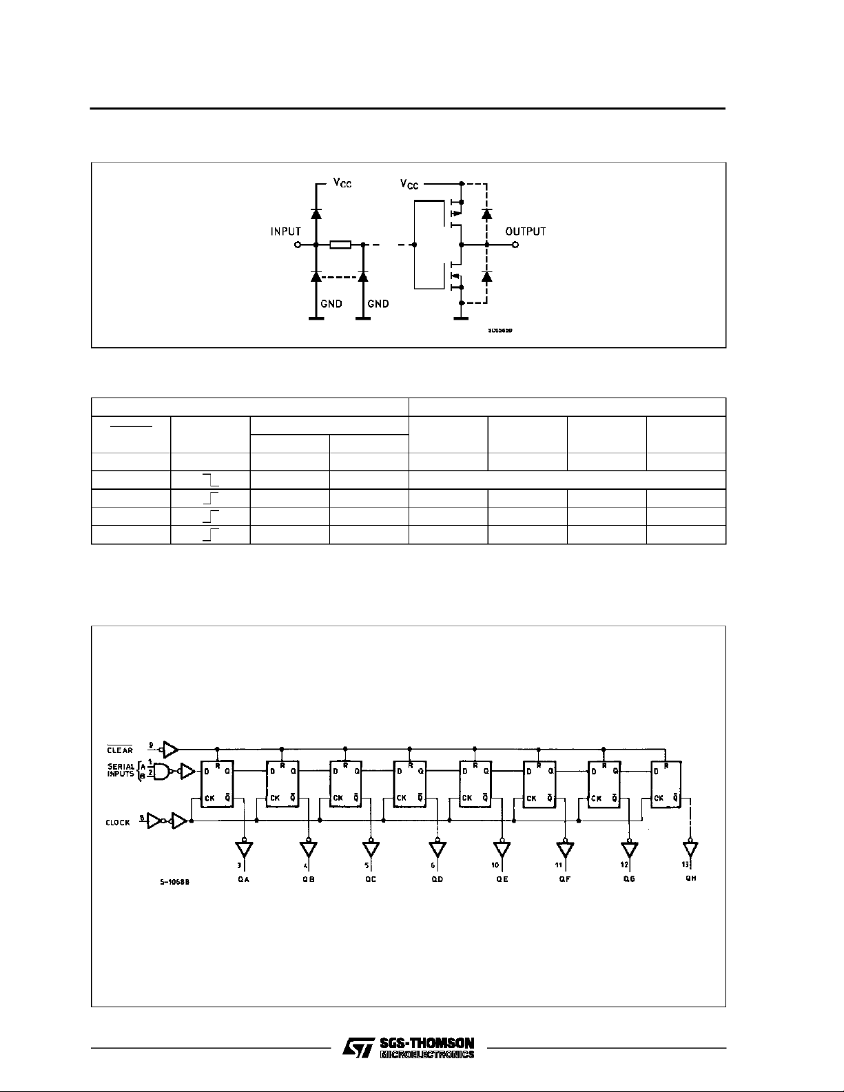
The HC164 is an 8 bit shiftregister with serialdata
entry and an output from each of the eight stages.
Data isentered serially through one oftwo inputs (A
or B), either of theseinputs canbeused asanactive
high enable for data entry through the other input.
An unused input must be high, or both inputs connected together. Each low-to-high transition on the
clock input shifts data one place to the right and
entersintoQA,thelogicNANDofthe twodata inputs
(A ⋅ B), the data that existed before the rising clock
edge. A low level on the clear input overrides all
otherinputsand clearstheregister asynchronously,
forcingall Q outputslow.
All inputs are equipped with protection circuits
against static discharge and transient excess voltage.
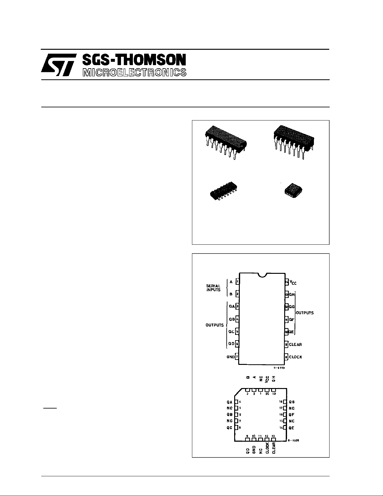
PIN CONNECTIONS(top view)
NC =
No Internal
Connection
October 1992
1/12
M54/M74HC164
INPUT AND OUTPUT EQUIVALENT CIRCUIT
TRUTH TABLE
INPUTS OUTPUS
CLEAR CLOCK
LXXXLL
H X X NO CHANGE
H L X L QAn
H X L L QAn
H H H H QAn
X:Don’tCare
QAn- QGn : The levelof QA -QG,respectively. before themost-recent transition ofth clock.
SERIAL IN
AB
QA QB ............ QH
............
............
............
............
L
QGn
QGn
QGn
LOGI C DIAG RAM
2/12
M54/M74HC164
PIN DESCRIPTION
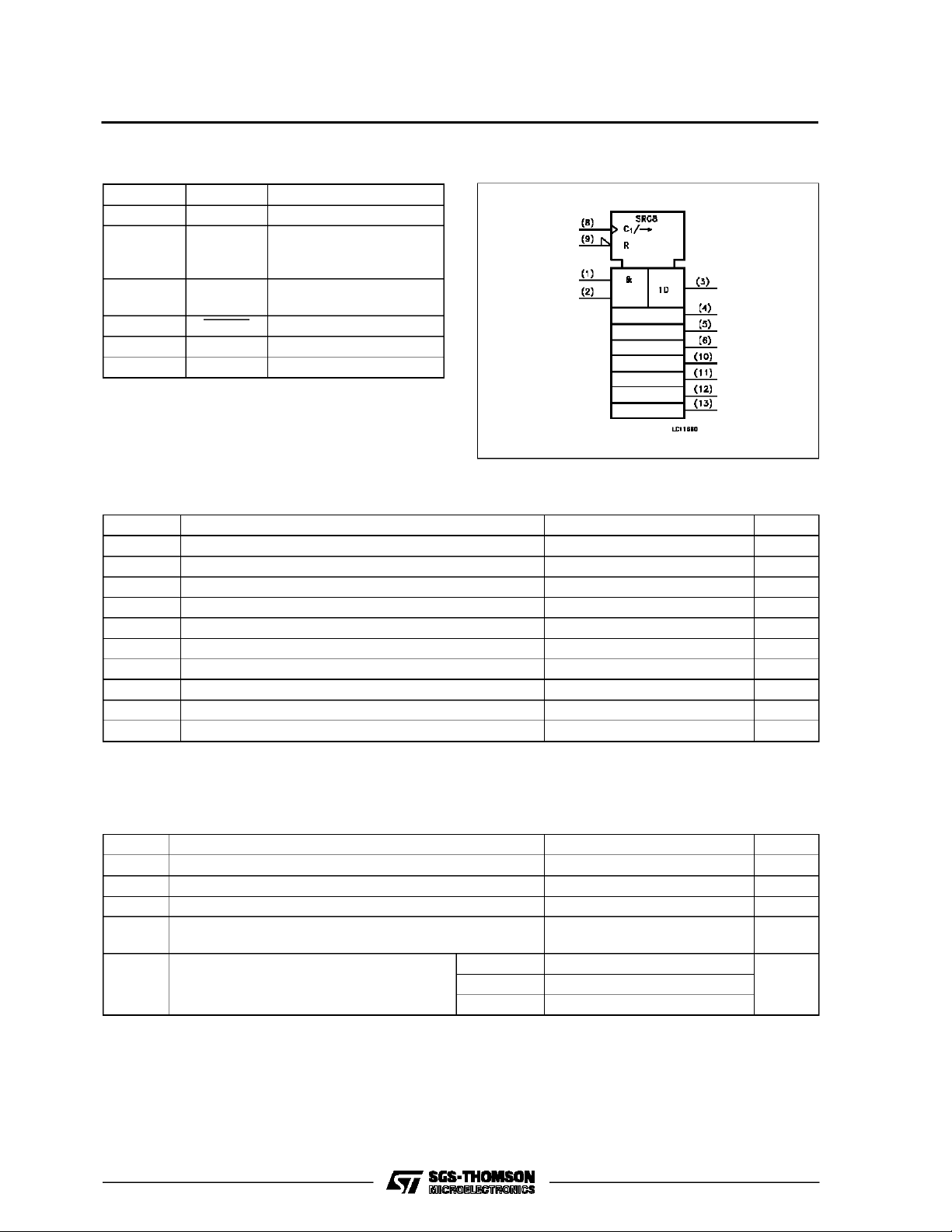
IEC LOGIC SYMBOL
PIN No SYMBOL NAME AND FUNCTION
1, 2 A, B Data Inputs
3, 4, 5, 6,
QA to QH Outputs
10, 11, 12,
13
8 CLOCK Clock Input (LOW to
HIGH, Edge-triggered)
9 CLEAR Master Reset Input
7 GND Ground (0V)
14 V
CC
Positive Supply Voltage
ABSOLU TE MAXIMU M RATINGS
Symbol Parameter Value Unit
V
CC
V
V
O
I
IK
I
OK
I
O
or I
I
CC
P
D
T
stg
T
L
AbsoluteMaximumRatingsarethose values beyond whichdamage tothedevicemayoccur. Functional operation under these conditionisnotimplied.
(*)500 mW: ≅ 65oC derateto300mWby 10mW/oC: 65oCto85oC
Supply Voltage -0.5 to +7 V
DC Input Voltage -0.5 to VCC+ 0.5 V
I
DC Output Voltage -0.5 to VCC+ 0.5 V
DC Input Diode Current ± 20 mA
DC Output Diode Current ± 20 mA
DC Output Source Sink Current Per Output Pin ± 25 mA
DC VCCor Ground Current ± 50 mA
GND
Power Dissipation 500 (*) mW
Storage Temperature -65 to +150
Lead Temperature (10 sec) 300
o
C
o
C
RECO MM ENDED O PERAT IN G C O NDITI O NS
Symbol Parameter Value Unit
V
V
T
t
V
r,tf
Supply Voltage 2 to 6 V
CC
Input Voltage 0 to V
I
Output Voltage 0 to V
O
Operating Temperature: M54HC Series
op
M74HC Series
CC
CC
-55 to +125
-40 to +85
Input Rise and Fall Time VCC= 2 V 0 to 1000 ns
V
= 4.5 V 0 to 500
CC
= 6 V 0 to 400
V
CC
V
V
o
C
o
C
3/12
M54/M74HC164
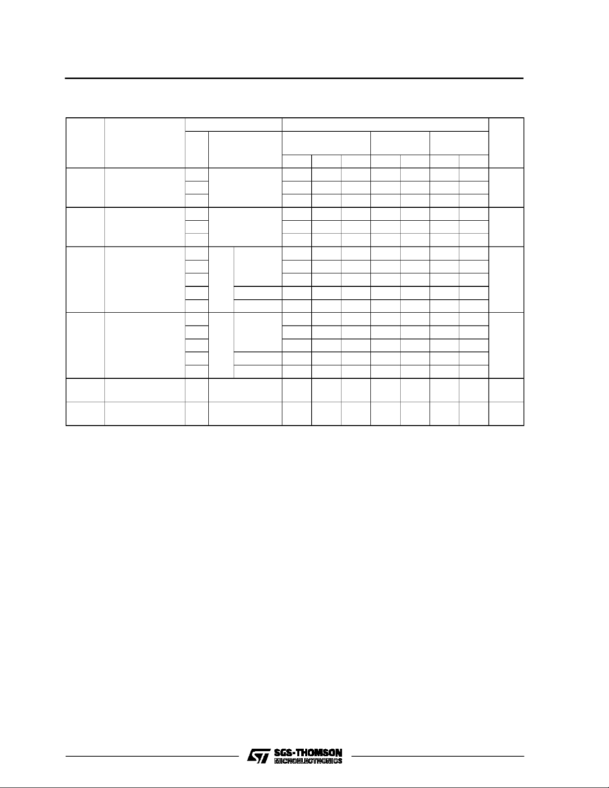
DC SPECIFICATIO NS
Symbol Parameter
V
V
V
V
I
High Level Input
IH
Voltage
Low Level Input
IL
Voltage
High Level
OH
Output Voltage
Low Level Output
OL
Voltage
I
Input Leakage
I
Current
Quiescent Supply
CC
Current
Test Conditions Value
V
(V)
CC
=25oC
A
54HC and 74HC
Min. Typ. Max. Min. Max. Min. Max.
-40 to 85oC
74HC
-55 to 125oC
54HC
Unit
T
2.0 1.5 1.5 1.5
4.5 3.15 3.15 3.15
6.0 4.2 4.2 4.2
2.0 0.5 0.5 0.5
4.5 1.35 1.35 1.35
6.0 1.8 1.8 1.8
2.0
4.5 4.4 4.5 4.4 4.4
6.0 5.9 6.0 5.9 5.9
4.5 I
6.0 I
2.0
4.5 0.0 0.1 0.1 0.1
6.0 0.0 0.1 0.1 0.1
4.5 I
6.0 I
6.0
=
V
I
IO=-20 µA
V
IH
or
V
IL
=-4.0 mA 4.18 4.31 4.13 4.10
O
=-5.2 mA 5.68 5.8 5.63 5.60
O
V
=
I
IO=20µA
V
IH
or
V
IL
= 4.0 mA 0.17 0.26 0.33 0.40
O
= 5.2 mA 0.18 0.26 0.33 0.40
O
VI=VCCor GND ±0.1 ±1 ±1 µA
1.9 2.0 1.9 1.9
0.0 0.1 0.1 0.1
6.0 VI=VCCor GND 4 40 80 µA
V
V
V
V
4/12
 Loading...