

4 TO 16 LINE DECODER/DEMULTIPLEXER
.HIGH SPEED
.t
= 15 ns(TYP.) at VCC=5V
PD
.LOWPOWERDISSIPATION
ICC=4µA(MAX.) at TA=25°C
.HIGH NOISEIMMUNITY
V
NIH=VNIL
=28%VCC(MIN.)
.OUTPUT DRIVE CAPABILITY
15 LSTTL LOADS
.SYMMETRICALOUTPUT IMPEDANCE
IOH =IOL= 4 mA (MIN.)
.BALANCEDPROPAGATION DELAYS
t
PLH=tPHL
.WIDE OPERATINGVOLTAGE RANGE
VCC(OPR)= 2V to 6 V
.PIN ANDFUNCTION COMPATIBLE
WITH 54/74LS154
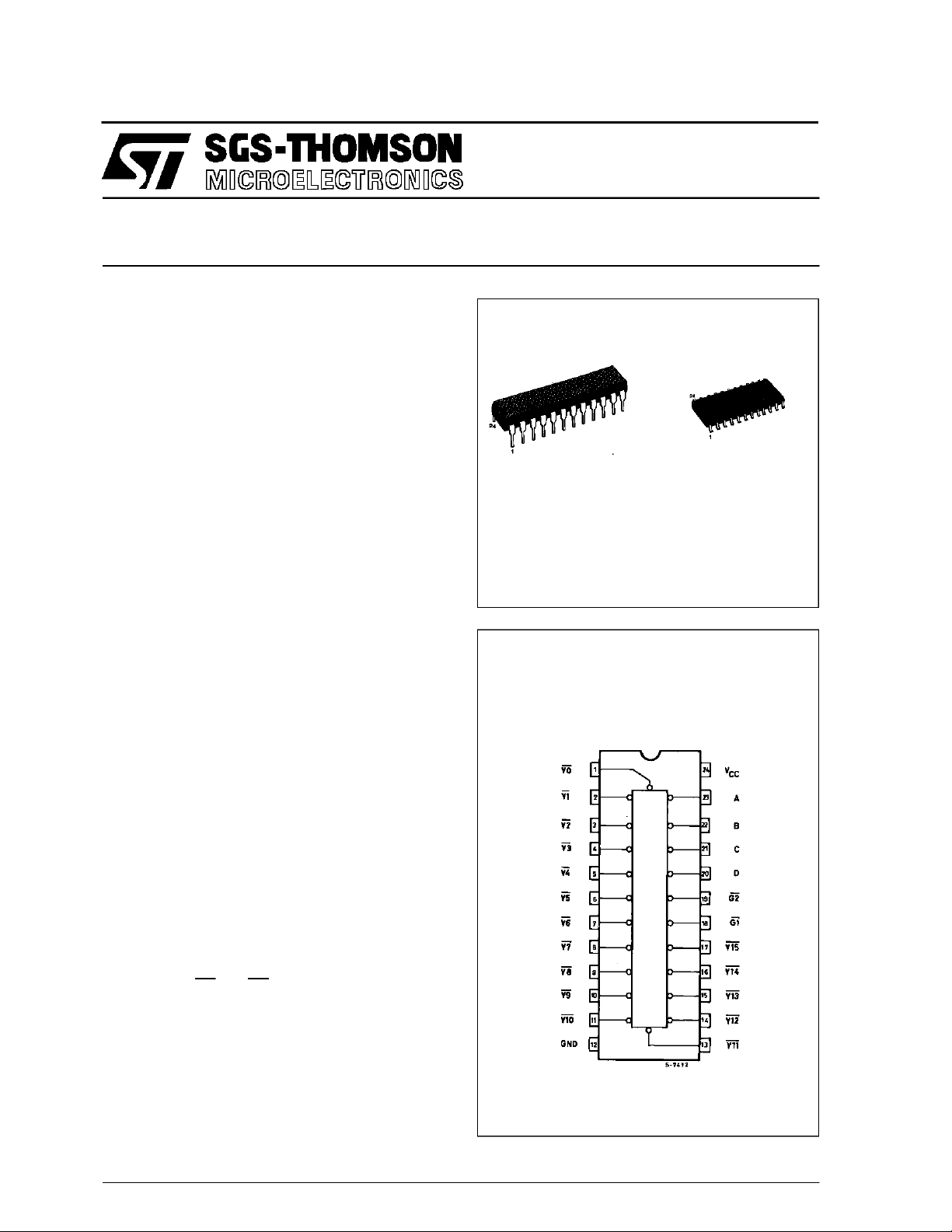
M74HC154
B1R
(PlasticPackage)
ORDER CODES :
M74HC 154B1R M74H C154M1R
M1R
(Micro Package)
DESCRIPTION
The74HC154 is ahigh speedCMOS4 TO 16-LINE
DECODER/DEMULTIPLEXER fabricated in silicon
gateC2MOStechnology. Ithasthe same high speed
performanceofLSTTLcombinedwithtrueCMOSlow
power consumption.
A binary code applied to the fourinputs (A toD) provides alow levelattheselectedoneofsixteenoutputs
excluding the other fifteen outputs, when both the
strobe inputs, G1 andG2, areheldlow. When either
strobe input isheldhigh,the decording function is inhibited to keep all outputs high. The strobe function
makes it easytoexpand the decoding lines through
cascading, and simplifies the design of address decoding circuits in memory controlsystems.
Allinputsareequipped withprotectioncircuitsagainst
staticdischarge and transient excess voltage.
NC =
No Internal
Connection
PIN CONNECTIONS(top view)
October 1993
1/8
M74HC154
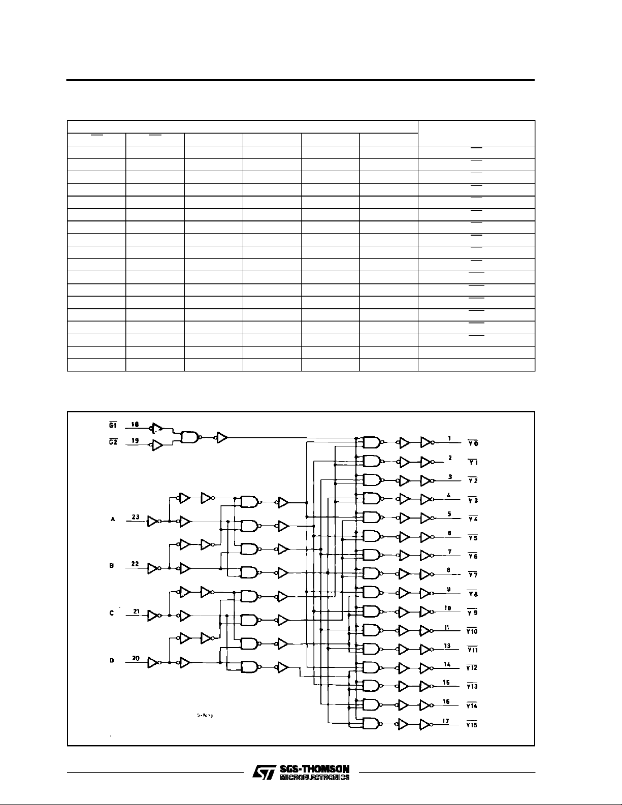
TRUTH TABLE
INPUTS SELECTED
G1 G2 D C B A
LLLLLL Y0
LLLLLH Y1
LLLLHL Y2
LLLLHH Y3
LLLHLL Y4
LLLHLH Y5
LLLHHL Y6
LLLHHH Y7
LLHLLL Y8
LLHLLH Y9
L L H L H L Y10
L L H L H H Y11
LLHHLL Y12
L L H H L H Y13
L L H H H L Y14
LLHHHH Y15
X H X X X X NONE
H X X X X X NONE
X: Don’t Care
OUTPUT (L)
LOGIC DIAGRAM
2/8
M74HC154
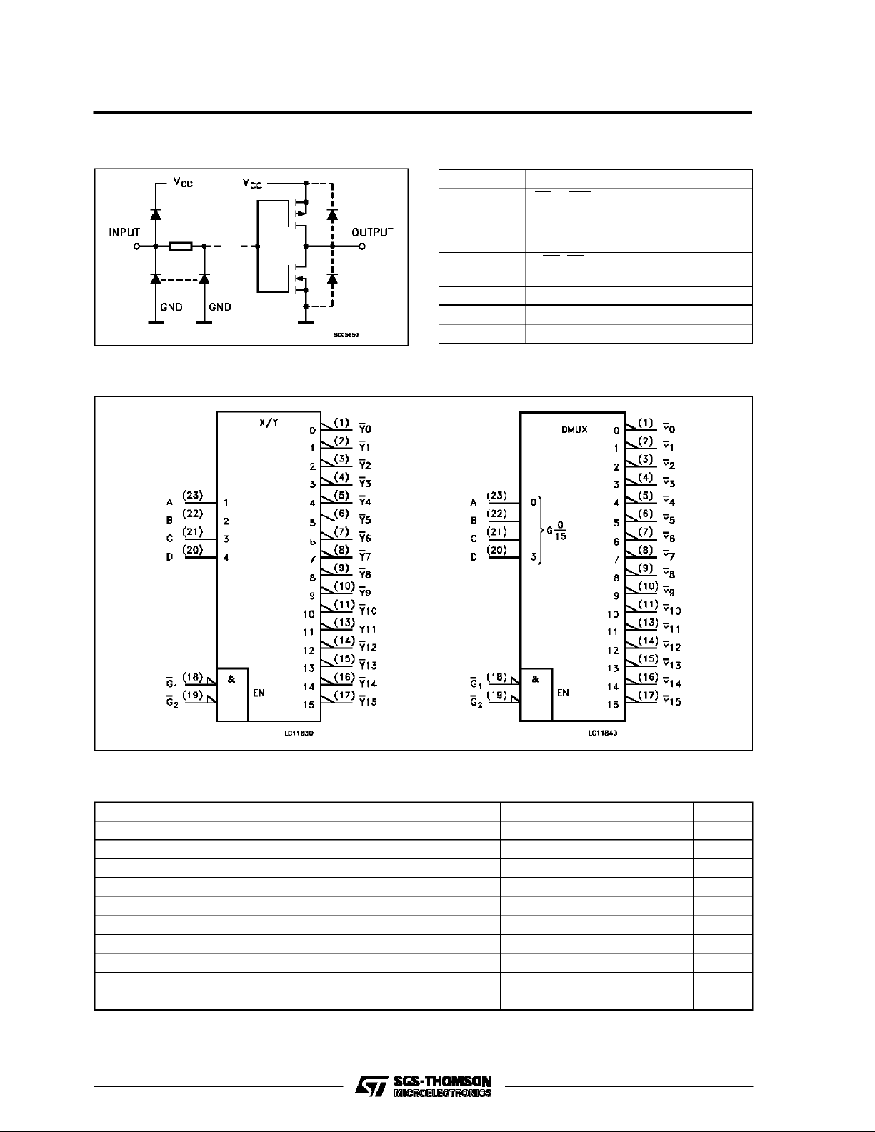
INPUT AND OUTPUT EQUIVALENT CIRCUIT
IEC LOGIC SYMBOLS
PIN DESCRIPTION
PIN No SYMBOL NAME AND FUNCTION
1, 2, 3, 4, 5,
6, 7, 8, 9, 10,
11, 13, 14,
15, 16, 17
18, 19 G1, G2 Enable Inputs (Active
23, 22, 21, 20 A to D Address Inputs
12 GND Ground (0V)
24 V
Y0 to Y15 Outputs (Active LOW)
LOW)
CC
Positive Supply Voltage
ABSOLU TE MAXIMU M RAT INGS
Symbol Parameter Value Unit
V
CC
V
V
O
I
IK
I
OK
I
O
or I
I
CC
P
D
T
stg
T
L
AbsoluteMaximumRatingsarethose values beyond whichdamage tothedevicemayoccur. Functional operation under these conditionisnotimplied.
(*)500 mW: ≅ 65oC derateto300mWby 10mW/oC: 65oCto85oC
Supply Voltage -0.5 to +7 V
DC Input Voltage -0.5 to VCC+ 0.5 V
I
DC Output Voltage -0.5 to VCC+ 0.5 V
DC Input Diode Current ± 20 mA
DC Output Diode Current ± 20 mA
DC Output Source Sink Current Per Output Pin ± 25 mA
DC VCCor Ground Current ± 50 mA
GND
Power Dissipation 500 (*) mW
Storage Temperature -65 to +150
Lead Temperature (10 sec) 300
o
C
o
C
3/8
 Loading...