

SGS Thomson Microelectronics M74HC14TTR, M74HC14RM13TR, M74HC14M1R, M74HC14B1R Datasheet
M74HC14
HEX SCHMITT INVER TER
■ HIGH SPEED:
t
=12ns (TYP.) at VCC = 6V
PD
■ LOW POWER DISSIPATION:
I
= 1µA(MAX.) at TA=25°C
CC
■ HIGH NOISE IMMUNITY:
V
= 1.2 V (TYP.) AT V
H
■ SYMMETRICAL OUTPUT IMPEDANCE:
|I
| = IOL = 4mA (MIN)
OH
■ BALANCED PROPAGATION DELAYS:
t
≅ t
PLH
■ WIDE OPERATING VOLTAGE RANGE:
V
CC
■ PIN AND FUNCTION COMPATIBLE WITH
PHL
(OPR) = 2V to 6V
CC =
6 V
74 SERIES 14
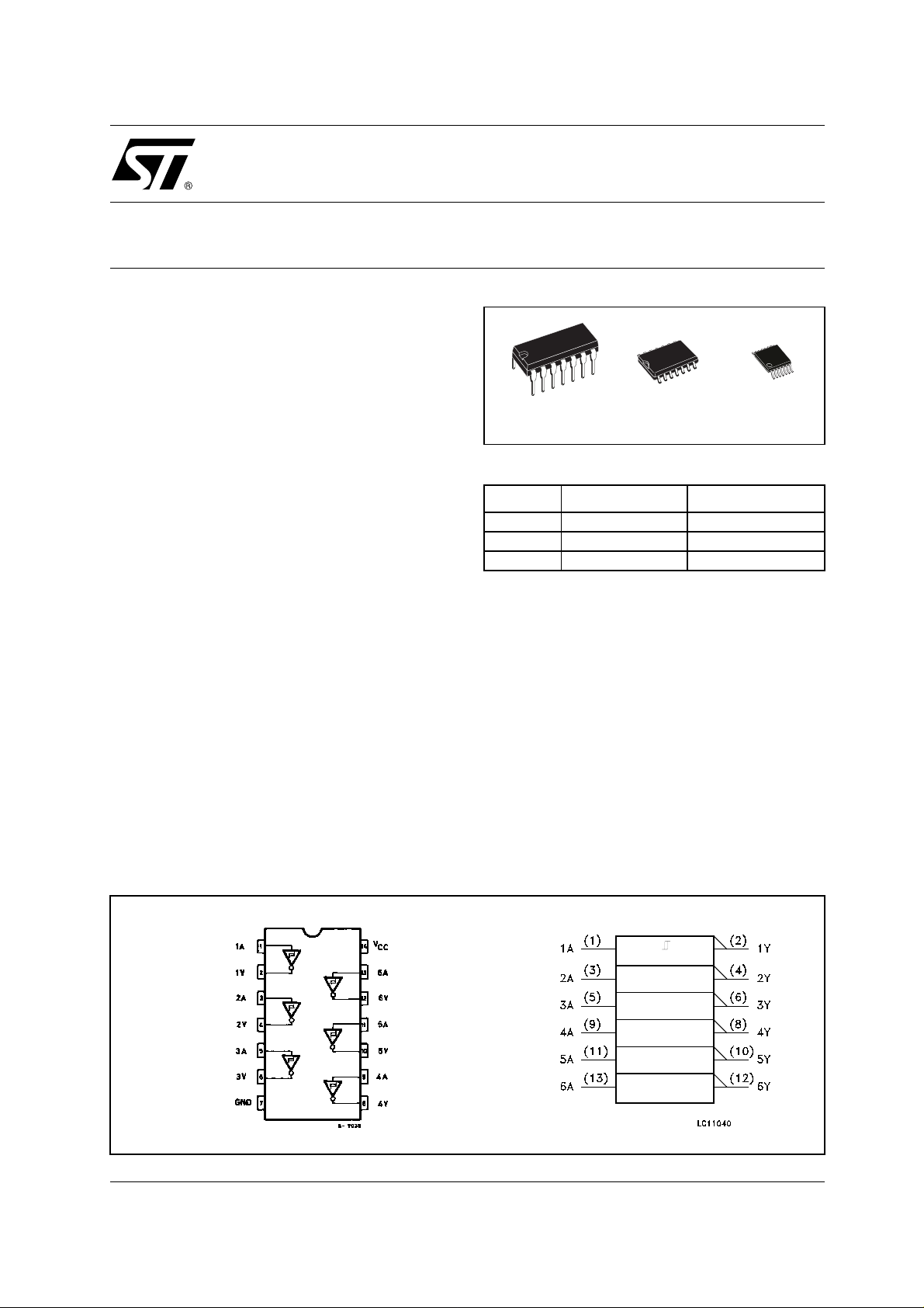
DESCRIPTION
The M74HC14 is an high speed CMOS HEX
SCHMI TT IN VE RTER fabr icat ed with s ilicon ga te
2
MOS technology. Pin configuration and
C
function are the same as those of the M74HC04
but all inputs have 20% V
hysteresis level.
cc
This, together with its schmitt trigger function,
allows it to be used on line receivers with slow
rise/fall input signals.
TSSOPDIP SOP
ORDER CODES
PACKAGE TUBE T & R
DIP M74HC14B1R
SOP M74HC14M1R M74HC14RM13TR
TSSOP M74HC14TTR
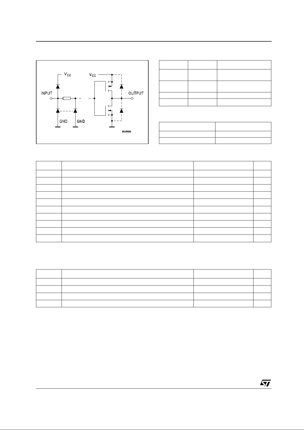
All inputs are equipped with protection circuits
against static discharge and transient excess
voltage.
PIN CONNECTION AND IEC LOGIC SYMBOLS
1/8July 2001
M74HC14
INPUT AND OUTPUT EQUIVALENT CIRCUIT PIN DESCRIPTION
PIN No SYMBOL NAME AND FUNCTION
1, 3, 5, 9, 1 1,
13
2, 4, 6, 8, 10,
12
7 GND Ground (0V)
14
TRUTH TABLE
ABSOLUTE MAXIMUM RATINGS
Symbol Parameter Value Unit
V
V
V
I
I
OK
I
I
or I
CC
P
T
T
Absolute Maximum Ratings are those values beyond which damage to the device may occur. Functional operation under these conditions is
not implied
(*) 500mW at 65
Supply Voltage
CC
DC Input Voltage -0.5 to VCC + 0.5
I
DC Output Voltage -0.5 to VCC + 0.5
O
DC Input Diode Current
IK
DC Output Diode Current
DC Output Current
O
DC VCC or Ground Current
GND
Power Dissipation
D
Storage Temperature
stg
Lead Temperature (10 sec)
L
°C; derate to 300mW by 10 m W/°C from 65 °C to 85°C
1A to 6A Data Inputs
1Y to 6Y Data Outputs
V
CC
Positive Supply Voltage
AY
LH
HL
-0.5 to +7 V
V
V
± 20 mA
± 20 mA
± 25 mA
± 50 mA
500(*) mW
-65 to +150 °C
300 °C
RECOMMENDED OPERATING CONDITIONS
Symbol Parameter Value Unit
V
V
V
T
2/8
Supply Voltage
CC
Input Voltage 0 to V
I
Output Voltage 0 to V
O
Operating Temperature
op
2 to 6 V
CC
CC
-55 to 125 °C
V
V
DC SPECIFICATIONS
Symbol Parameter
V
High Level Input
t+
Voltage
Low Level Input
V
t-
Voltage
Hysteresis Voltage 2.0 0.3 0.54 1.0 0.3 1.0 0.3 1.0
V
H
V
V
I
High Level Output
OH
Voltage
Low Level Output
OL
Voltage
I
Input Leakage
I
Current
Quiescent Supply
CC
Current
M74HC14
Test Condition Value
= 25°C
T
V
CC
(V)
A
Min. Typ. Max. Min. Max. Min. Max.
2.0 1.0 1.28 1.5 1.0 1.5 1.0 1.5
6.0 3.0 3.7 4.2 3.0 4.2 3.0 4.2
2.0 0.3 0.74 0.9 0.3 0.9 0.3 0.9
6.0 1.5 2.4 2.6 1.5 2.6 1.5 2.6
6.0 0.8 1.3 1.4 0.8 1.7 0.8 1.7
2.0
4.5
6.0
4.5
6.0
2.0
4.5
6.0
4.5
6.0
6.0
6.0
IO=-20 µA
I
=-20 µA
O
I
=-20 µA
O
I
=-4.0mA
O
I
=-5.2 mA
O
=-20 µA
I
O
I
=-20 µA
O
I
=-20 µA
O
I
=-4.0mA
O
I
=-5.2 mA
O
= VCC or GND
V
I
= VCC or GND
V
I
1.9 2.0 1.9 1.9
4.4 4.5 4.4 4.4
5.9 6.0 5.9 5.9
4.18 4.31 4.13 4.10
5.68 5.8 5.63 5.60
0.0 0.1 0.1 0.1
0.0 0.1 0.1 0.1
0.0 0.1 0.1 0.1
0.17 0.26 0.33 0.40
0.18 0.26 0.33 0.40
-40 to 85°C -55 to 125°C
± 0.1 ± 1 ± 1 µA
11020µA
Unit
V4.5 2.3 2.8 3.15 2.3 3.15 2.3 3.15
V4.5 1.13 1.8 2.0 1.13 2.0 1.13 2.0
V4.5 0.6 1.0 1.4 0.6 1.4 0.6 1.4
V
V
AC ELECTRICAL CHARACTERISTICS (C
Test Condition Value
Symbol Parameter
t
TLH tTHL
t
PLH tPHL
Output Transition
Time
Propagation Delay
Time
V
CC
(V)
2.0 30 75 95 110
6.0 7131619
2.0 42 125 155 190
6.0 12 21 16 32
= 50 pF, Input tr = tf = 6ns)
L
= 25°C
T
A
Min. Typ. Max. Min. Max. Min. Max.
-40 to 85°C -55 to 125°C
Unit
ns4.5 8151922
ns4.5 14 25 31 38
3/8
 Loading...