

SGS Thomson Microelectronics M74HC138 Datasheet
3 TO8 LINE DECODER (INVERTING)
.HIGH SPEED
tPD= 16 ns(TYP.) AT VCC=5V
.LOWPOWERDISSIPATION
ICC=4µAATTA=25°C
.OUTPUTDRIVE CAPABILITY
10 LSTTL LOADS
.BALANCEDPROPAGATION DELAYS
t
PLH=tPHL
.SYMMETRICALOUTPUT IMPEDANCE
|IOH|=I
OL
.HIGH NOISE IMMUNITY
V
NIH=VNIL
=28%VCC(MIN.)
.WIDE OPERATINGVOLTAGE RANGE
VCC(OPR)= 2 V TO6 V
.PIN ANDFUNCTION COMPATIBLE
WITH 54/74LS138
DESCRIPTION
The M54/74HC138 is a high speed CMOS 3 TO 8
LINE DECODER fabricated in silicon gate C2MOS
technology.
It has the same high speed performance of LSTTL
combined withtrue CMOSlowpower consumption.
If the deviceis enabled, 3 binaryselect inputs (A,B
and C) determine which one of the outputs will go
low. If enableinput G1 is held low or either G2A or
G2B is held high,the decoding function is inhibited
and all the 8 outputs go high.
Three enable inputs are provided to ease cascade
connection and application ofaddress decoders for
memorysystems. All inputs are equipped with protection circuits against static discharge and transient excess voltage.
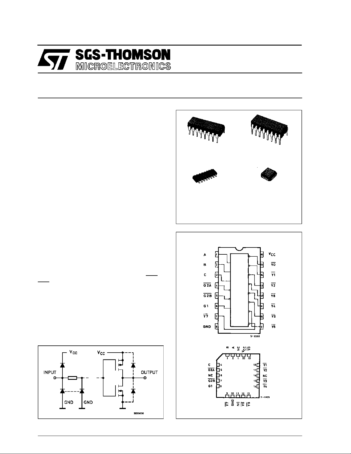
M54HC138
M74HC138
B1R
(PlasticPackage)
M1R
(MicroPackage)
ORDER CODES :
M54HC 138F1R M74H C138M1R
M74HC 138B1R M74HC1 38C1R
PIN CONNECTIONS(top view)
F1R
(CeramicPackage)
C1R
(Chip Carrier)
INPUT AND OUTPUT EQUIVALENT CIRCUIT
October 1992
NC =
No Internal
Connection
1/10
M54/M74HC138
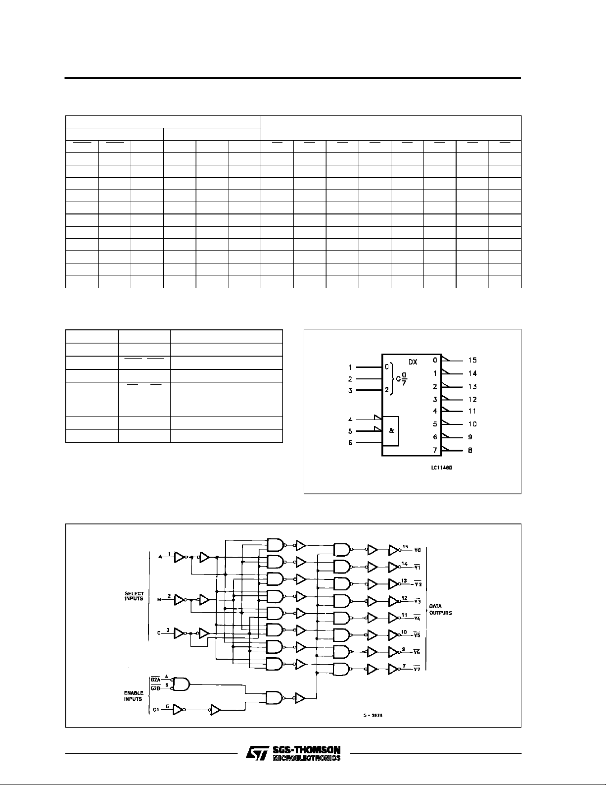
TRUTH TABLE
INPUTS
ENABLE SELECT
G2B G2A G1 C B A Y0 Y1 Y2 Y3 Y4 Y5 Y6 Y7
XXLXXXHHHHHHHH
XHXXXXHHHHHHHH
HXXXXXHHHHHHHH
LLHL L LLHHHHHHH
LLHL LHHLHHHHHH
LLHLHLHHLHHHHH
LLHLHHHHHLHHHH
LLHHL LHHHHLHHH
LLHHLHHHHHHLHH
LLHHHLHHHHHHLH
LLHHHHHHHHHHHL
X:Don’t Care
OUTPUTS
IEC LOGIC SYMBOLPIN DESCRIPTION
PIN No SYMBOL NAME AND FUNCTION
1, 2, 3 A, B, C Address Inputs
4, 5 G2A, G2B Enable Inputs
6 G1 Enable Input
15, 14, 13,
12, 11, 10,
9, 7
8 GND Ground (0V)
16 V
Y0 to Y7 Outputs
CC
Positive Supply Voltage
LOGI C DIAG RAM
2/10
M54/M74HC138
ABSOLU TE M AXI MU M R AT INGS
Symbol Parameter Value Unit
V
CC
V
V
O
I
IK
I
OK
I
O
I
or I
CC
P
D
T
stg
T
AbsoluteMaximumRatingsarethose values beyondwhichdamage tothedevicemayoccur. Functionaloperationunder these conditionisnotimplied.
(*)500 mW: ≅ 65oC derateto300mWby 10mW/oC: 65oCto85oC
RECO MM ENDED O PERAT IN G CONDI TIONS
Symbol Parameter Value Unit
V
CC
V
I
V
O
T
op
t
r,tf
Supply Voltage -0.5 to +7 V
DC Input Voltage -0.5 to VCC+ 0.5 V
I
DC Output Voltage -0.5 to VCC+ 0.5 V
DC Input Diode Current ± 20 mA
DC Output Diode Current ± 20 mA
DC Output Source Sink Current Per Output Pin ± 25 mA
DC VCCor Ground Current ± 50 mA
GND
Power Dissipation 500 (*) mW
Storage Temperature -65 to +150
Lead Temperature (10 sec) 300
L
Supply Voltage 2 to 6 V
Input Voltage 0 to V
Output Voltage 0 to V
Operating Temperature: M54HC Series
M74HC Series
CC
CC
-55 to +125
-40 to +85
Input Rise and Fall Time VCC= 2 V 0 to 1000 ns
V
= 4.5 V 0 to 500
CC
= 6 V 0 to 400
V
CC
o
C
o
C
V
V
o
C
o
C
3/10
 Loading...