

Datasheet M74HC137M1R, M74HC137C1R, M74HC137B1R, M74HC137, M54HC137F1R Datasheet (SGS Thomson Microelectronics)
3 TO8 LINE DECODER/LATCH (INVERTING)
.HIGH SPEED
tPD= 11 ns(TYP.) AT VCC=5V
.LOWPOWER DISSIPATION
ICC=4µA(MAX.) AT TA=25 °C
.HIGH NOISE IMMUNITY
V
NIH=VNIL
=28%VCC(MIN.)
.OUTPUT DRIVE CAPABILITY
10 LSTTLLOADS
.SYMMETRICALOUTPUT IMPEDANCE
IOH =IOL= 4 mA(MIN.)
.BALANCEDPROPAGATION DELAYS
t
PLH=tPHL
.WIDE OPERATINGVOLTAGE RANGE
VCC(OPR)= 2 V TO6 V
.PIN ANDFUNCTION COMPATIBLE
WITH 54/74LS137
DESCRIPTION
The M54/74HC137 i sahigh speedCMOS 3TO 8LINE
DECODER/LATCH (INVERTING)fabricated in silicon
gate C2MOS technology. It has the same high speed
performance ofLSTTLcombined withtrueCMOSlow
power consumption. This device is a 3 to 8line d ecoder
withlatches on thethree address inputs. WhenGLgoes
from lowtohigh, theaddress present attheselectinputs
(A,BandC)isstoredinthelatches.AslongasGLremains high noaddress changes will berecognized. Output enable pins G1 and G2, control the state of the
outputs independently of the select or latch-enable inputs. All the outputs are high unless G1is high and G2
is low. The HC137is idea lly suited for the implemen tation of glitch-free decoders in stored-address applications in bus oriented systems. All inputs are equipped
withprotection circuitsagainst staticdischarge andtransient excess voltage.
M54HC137
M74HC137
B1R
(PlasticPackage)
M1R
(MicroPackage)
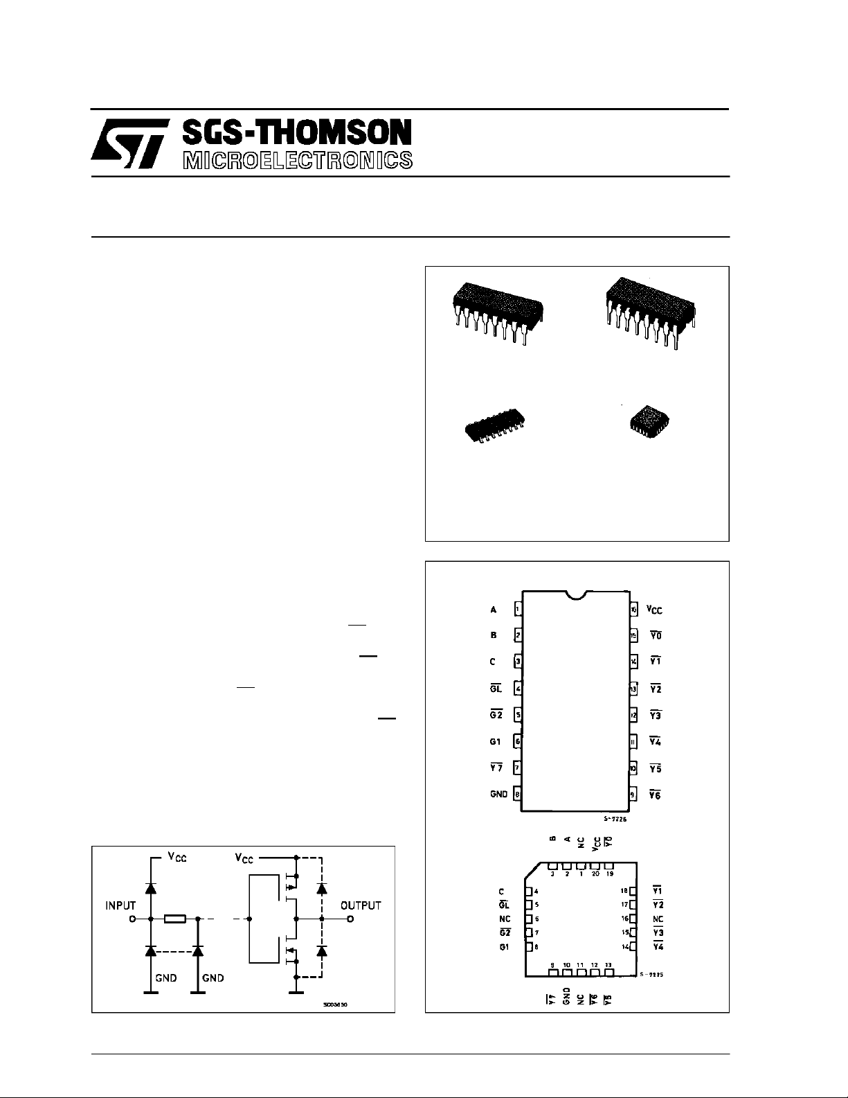
ORDER CODES :
M54HC 137F1R M74H C137M1R
M74HC 137B1R M74HC1 37C1R
PIN CONNECTIONS (top view)
F1R
(CeramicPackage)
C1R
(Chip Carrier)
INPUT AND OUTPUT EQUIVALENT CIRCUIT
February 1993
NC =
No Internal
Connection
1/11
M54/M74HC137
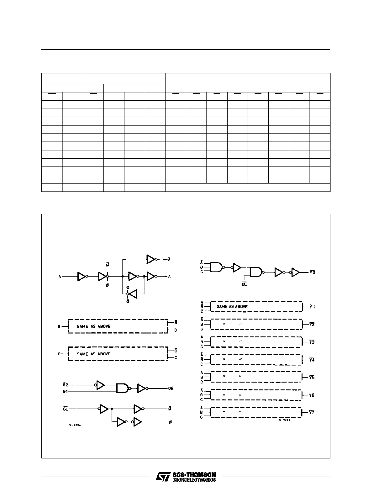
TRUTH TABLE
INPUTS
ENABLE SELECT
GL G1 G2 C B A Y0 Y1 Y2 Y3 Y4 Y5 Y6 Y7
XXHXXXHHHHHHHH
XLXXXXHHHHHHHH
LHL L L LLHHHHHHH
LHL L LHHLHHHHHH
LHL LHLHHLHHHHH
LHL LHHHHHLHHHH
LHLHL LHHHHLHHH
LHLHLHHHHHHLHH
LHLHHLHHHHHHLH
LHLHHHHHHHHHHL
H H L X X X Outputs corresponding to stored address L: all others H
OUTPUTS
LOGI C DIAG RAM
2/11
PIN DESCRIPTION
PIN No SYMBOL NAME AND FUNCTION
1, 2, 3 A to C Data Inputs
4 GL Latch Enable Input (Active LOW)
5 G2 Data Enable Input (Active LOW)
6 G1 Data Enable Input (Active HIGH)
15, 14, 13, 12, 11, 10, 9, 7 Y0 to Y7 Multiplexer Outputs
8 GND Ground (0V)
16 V
CC
Positive Supply Voltage
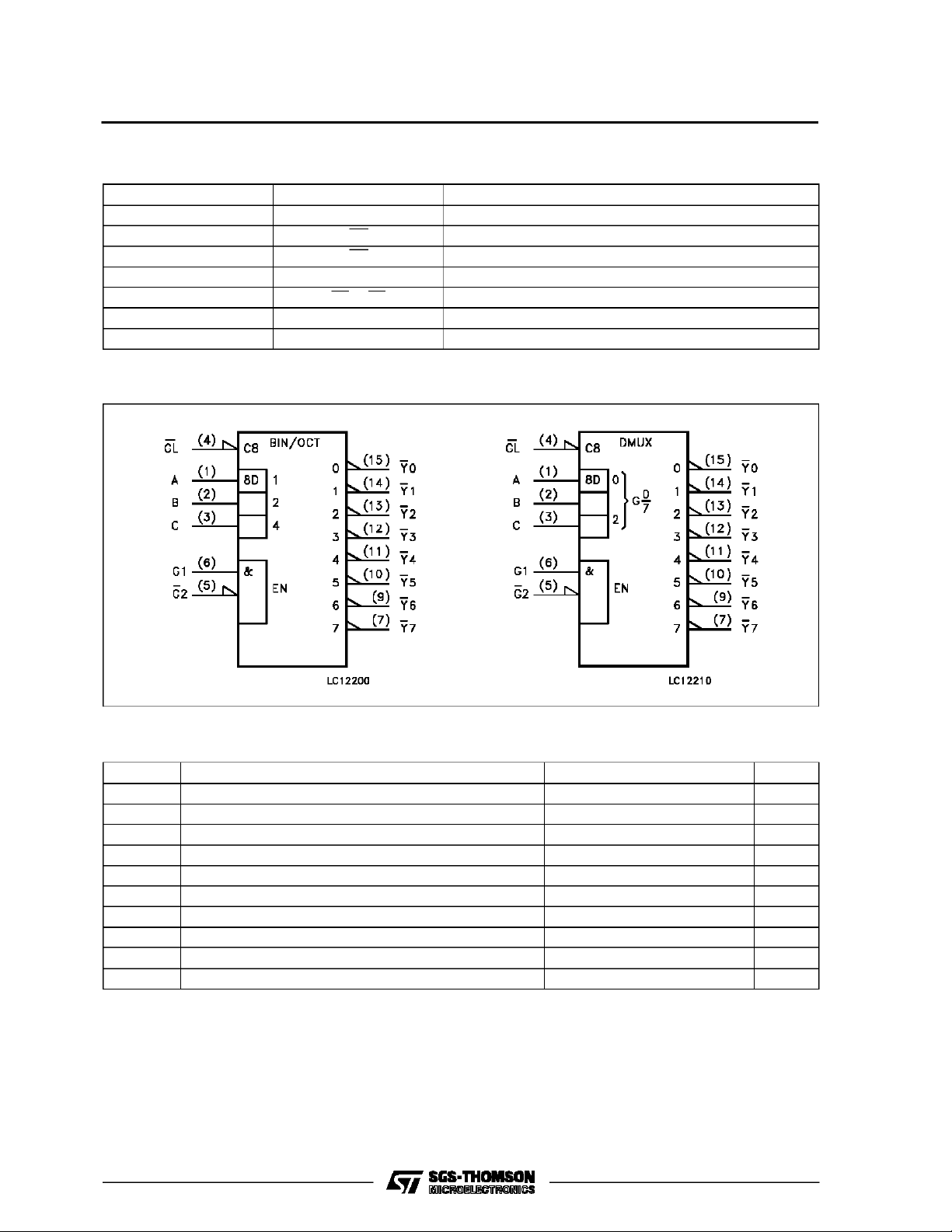
IEC LOGIC SYMBOLS
M54/M74HC137
ABSOLU TE M AXI MU M R AT INGS
Symbol Parameter Value Unit
V
CC
V
V
O
I
IK
I
OK
I
O
I
or I
CC
P
D
T
stg
T
AbsoluteMaximumRatingsarethosevaluesbeyond whichdamagetothedevicemayoccur.Functional operationunder theseconditionisnotimplied.
(*)500 mW:≅ 65oC derateto 300 mWby 10mW/oC: 65oCto85oC
Supply Voltage -0.5 to +7 V
DC Input Voltage -0.5 to VCC+ 0.5 V
I
DC Output Voltage -0.5 to VCC+ 0.5 V
DC Input Diode Current ± 20 mA
DC OutputDiode Current ± 20 mA
DC Output Source Sink Current Per Output Pin ± 25 mA
DC VCCor Ground Current ± 50 mA
GND
Power Dissipation 500 (*) mW
Storage Temperature -65 to +150
Lead Temperature (10 sec) 300
L
o
C
o
C
3/11
M54/M74HC137
RECO MM ENDED OPERATI N G CO NDITI O NS
Symbol Parameter Value Unit
V
V
V
T
t
r,tf
DC SPECIFICATIO NS
Symbol Parameter
V
IH
V
V
OH
V
OL
I
I
CC
Supply Voltage 2 to 6 V
CC
Input Voltage 0 to V
I
Output Voltage 0 to V
O
Operating Temperature: M54HC Series
op
M74HC Series
CC
CC
-55 to +125
-40 to +85
Input Rise and Fall Time VCC= 2 V 0 to 1000 ns
V
= 4.5 V 0 to 500
CC
V
= 6 V 0 to 400
CC
Test Conditions Value
V
(V)
CC
=25oC
T
A
54HC and 74HC
-40 to 85oC
74HC
-55 to 125oC
Min. Typ. Max. Min. Max. Min. Max.
High Level Input
Voltage
2.0 1.5 1.5 1.5
4.5 3.15 3.15 3.15
6.0 4.2 4.2 4.2
Low Level Input
IL
Voltage
2.0 0.5 0.5 0.5
4.5 1.35 1.35 1.35
6.0 1.8 1.8 1.8
High Level
Output Voltage
Low Level Output
Voltage
Input Leakage
I
Current
Quiescent Supply
2.0
V
=
I
4.5 4.4 4.5 4.4 4.4
6.0 5.9 6.0 5.9 5.9
4.5 I
6.0 I
2.0
4.5 0.0 0.1 0.1 0.1
6.0 0.0 0.1 0.1 0.1
4.5 I
6.0 I
6.0
IO=-20 µA
V
IH
or
V
IL
=-4.0 mA 4.18 4.31 4.13 4.10
O
=-5.2 mA 5.68 5.8 5.63 5.60
O
V
=
I
IO=20µA
V
IH
or
V
IL
= 4.0 mA 0.17 0.26 0.33 0.40
O
= 5.2 mA 0.18 0.26 0.33 0.40
O
VI=VCCor GND ±0.1 ±1 ±1 µA
1.9 2.0 1.9 1.9
0.0 0.1 0.1 0.1
6.0 VI=VCCor GND 2 20 40 µA
Current
54HC
V
V
o
C
o
C
Unit
V
V
V
V
4/11

M54/M74HC137
AC ELECTRICAL CHARACTERISTICS (CL=50pF,Inputtr=tf=6ns)
Test Conditions Value
T
=25oC
Symbol Parameter
t
t
TLH
THL
Output Transition
Time
V
CC
(V)
2.0 30 75 95 110
4.5 8151922
A
54HC and 74HC
Min. Typ. Max. Min. Max. Min. Max.
6.0 7131619
t
PLH
t
PHL
Propagation
Delay Time
(G1 - Y)
t
t
PLH
PHL
Propagation
Delay Time
(G2 - Y)
t
t
PLH
PHL
Propagation
Delay Time
(GL - Y)
t
t
PLH
PHL
Propagation
Delay Time
(A, B, C - Y)
t
W(L)
Minimum Pulse
Width
(GL)
Minimum Set-up
t
s
Time
(A, B, C - GL)
t
Minimum Hold
h
Time
(A, B, C - GL)
C
C
PD
Input Capacitance 5 10 10 10 pF
IN
(*) Power Dissipation
2.0 45 115 145 175
4.5 14 23 29 35
6.0 12 20 25 30
2.0 50 115 145 175
4.5 15 23 29 35
6.0 13 20 25 30
2.0 70 170 215 250
4.5 22 34 43 50
6.0 19 29 37 43
2.0 70 165 205 110
4.5 21 33 41 22
6.0 18 28 35 19
2.0 12 50 65 75
4.5 3101315
6.0 3 9 11 13
2.0 8506075
4.5 2101215
6.0 2 9 10 13
2.0 5 5 5
4.5 5 5 5
6.0 5 5 5
55
Capacitance
(*) CPDisdefined as the valueof the IC’s internal equivalent capacitance which is calculated fromthe operatingcurrent consumption withoutload.
(Referto Test Circuit).Average opertingcurrentcanbe obtained by the followingequation. ICC(opr) = CPD•VCC•fIN+I
-40 to 85oC
74HC
-55 to 125oC
54HC
CC
Unit
ns
ns
ns
ns
ns
ns
ns
ns
pF
5/11

M54/M74HC137
TEST CIRCUIT ICC(Opr.)
INPUTWAVEFORM IS THE SAME AS THAT IN CASE OF SWITCHINGCHARACTERISTICSTEST.
TYPICAL APPLICATION
6/11

Plastic DIP16 (0.25) MECHANICAL DATA
M54/M74HC137
DIM.
MIN. TYP. MAX. MIN. TYP. MAX.
a1 0.51 0.020
B 0.77 1.65 0.030 0.065
b 0.5 0.020
b1 0.25 0.010
D 20 0.787
E 8.5 0.335
e 2.54 0.100
e3 17.78 0.700
F 7.1 0.280
I 5.1 0.201
L 3.3 0.130
Z 1.27 0.050
mm inch
P001C
7/11

M54/M74HC137
Ceramic DIP16/1 MECHANICAL DATA
DIM.
MIN. TYP. MAX. MIN. TYP. MAX.
A 20 0.787
B 7 0.276
D 3.3 0.130
E 0.38 0.015
e3 17.78 0.700
F 2.29 2.79 0.090 0.110
G 0.4 0.55 0.016 0.022
H 1.17 1.52 0.046 0.060
L 0.22 0.31 0.009 0.012
M 0.51 1.27 0.020 0.050
N 10.3 0.406
P 7.8 8.05 0.307 0.317
Q 5.08 0.200
mm inch
8/11
P053D

SO16 (Narrow) MECHANICAL DATA
M54/M74HC137
DIM.
MIN. TYP. MAX. MIN. TYP. MAX.
A 1.75 0.068
a1 0.1 0.2 0.004 0.007
a2 1.65 0.064
b 0.35 0.46 0.013 0.018
b1 0.19 0.25 0.007 0.010
C 0.5 0.019
c1 45° (typ.)
D 9.8 10 0.385 0.393
E 5.8 6.2 0.228 0.244
e 1.27 0.050
e3 8.89 0.350
F 3.8 4.0 0.149 0.157
G 4.6 5.3 0.181 0.208
L 0.5 1.27 0.019 0.050
M 0.62 0.024
S8°(max.)
mm inch
P013H
9/11

M54/M74HC137
PLCC20 MECHANICAL DATA
DIM.
MIN. TYP. MAX. MIN. TYP. MAX.
A 9.78 10.03 0.385 0.395
B 8.89 9.04 0.350 0.356
D 4.2 4.57 0.165 0.180
d1 2.54 0.100
d2 0.56 0.022
E 7.37 8.38 0.290 0.330
e 1.27 0.050
e3 5.08 0.200
F 0.38 0.015
G 0.101 0.004
M 1.27 0.050
M1 1.14 0.045
mm inch
10/11
P027A

M54/M74HC137
Information furnished is believed to be accurate and reliable. However, SGS-THOMSON Microelectronics assumes no responsability for the
consequences of use of such information nor for any infringement of patents or other rights of third parties which may results from its use. No
license is granted byimplication or otherwise under any patent or patentrights of SGS-THOMSON Microelectronics. Specificationsmentioned
in this publication are subject to change without notice. This publication supersedes and replaces all information previously supplied.
SGS-THOMSON Microelectronicsproducts are not authorized foruse ascritical componentsin life support devices orsystems without express
written approval of SGS-THOMSON Microelectonics.
1994 SGS-THOMSON Microelectronics - All Rights Reserved
Australia - Brazil - France - Germany - Hong Kong - Italy - Japan - Korea - Malaysia - Malta - Morocco - The Netherlands -
Singapore -Spain - Sweden- Switzerland -Taiwan - Thailand - UnitedKingdom - U.S.A
SGS-THOMSON Microelectronics GROUP OF COMPANIES
11/11
 Loading...