

.HIGH SPEED
tPD= 8 ns (TYP.) AT VCC=5V
.LOWPOWER DISSIPATION
ICC=4µA(MAX.) AT 25 °C
.OUTPUT DRIVE CAPABILITY
15 LSTTL LOADS
.BALANCEDPROPAGATION DELAYS
t
PLH=tPHL
.SYMMETRICALOUTPUT IMPEDANCE
IOL=IOH = 6 mA (MIN.)
.HIGH NOISEIMMUNITY
V
NIH=VNIL
=28%VCC(MIN.)
.WIDE OPERATING VOLTAGERANGE
VCC(OPR)= 2 V TO6 V
.PIN AND FUNCTION COMPATIBLE
WITH 54/74LS125/126
M54/74HC125
M54/74HC126
QUAD BUS BUFFERS (3-STATE)
B1R
(PlasticPackage)
M1R
(MicroPackage)
ORDER CODES :
M54HC X XXF1R M74H CXXXM1R
M74HC X XXB1R M74HCX X XC1R
F1R
(CeramicPackage)
C1R
(Chip Carrier)
DESCRIPTION
The M54/74HC125/126 are high speed CMOS
QUAD BUS BUFFER (3-STATE) FABRICATED IN
SILICON GATEC2MOS technology.
They have the same high speed performance of
LSTTL combined with true CMOS low power consumption.
These devices require the same 3-STATE control
inputG to betaken high to make the output go into
the high impedance state.
All inputs are equipped with protection circuits
against static discharge and transient excess voltage.
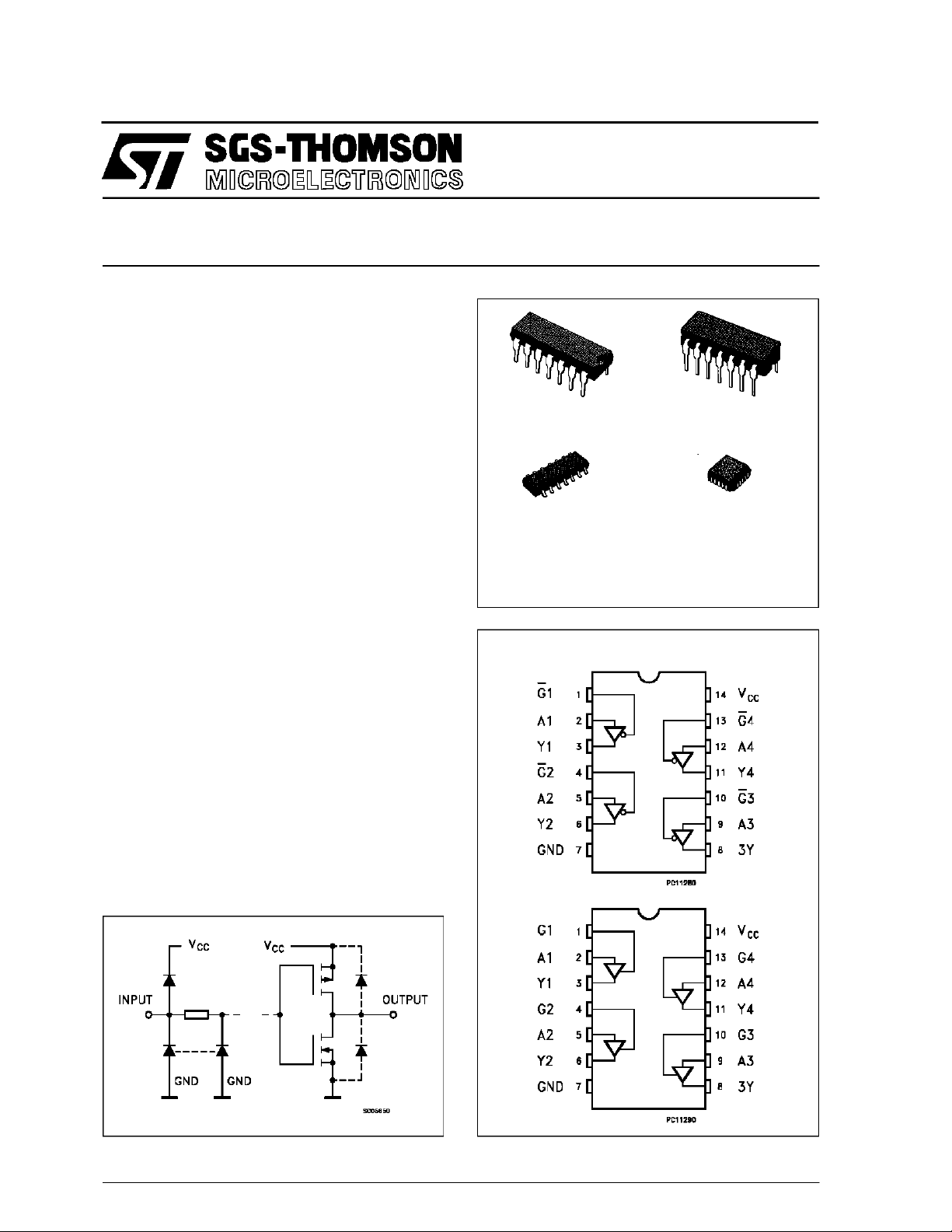
INPUT AND OUTPUT EQUIVALENT CIRCUIT
PIN CONNECTIONS(top view)
HC125
HC126
September 1993
NC =
No Internal
Connection
1/11
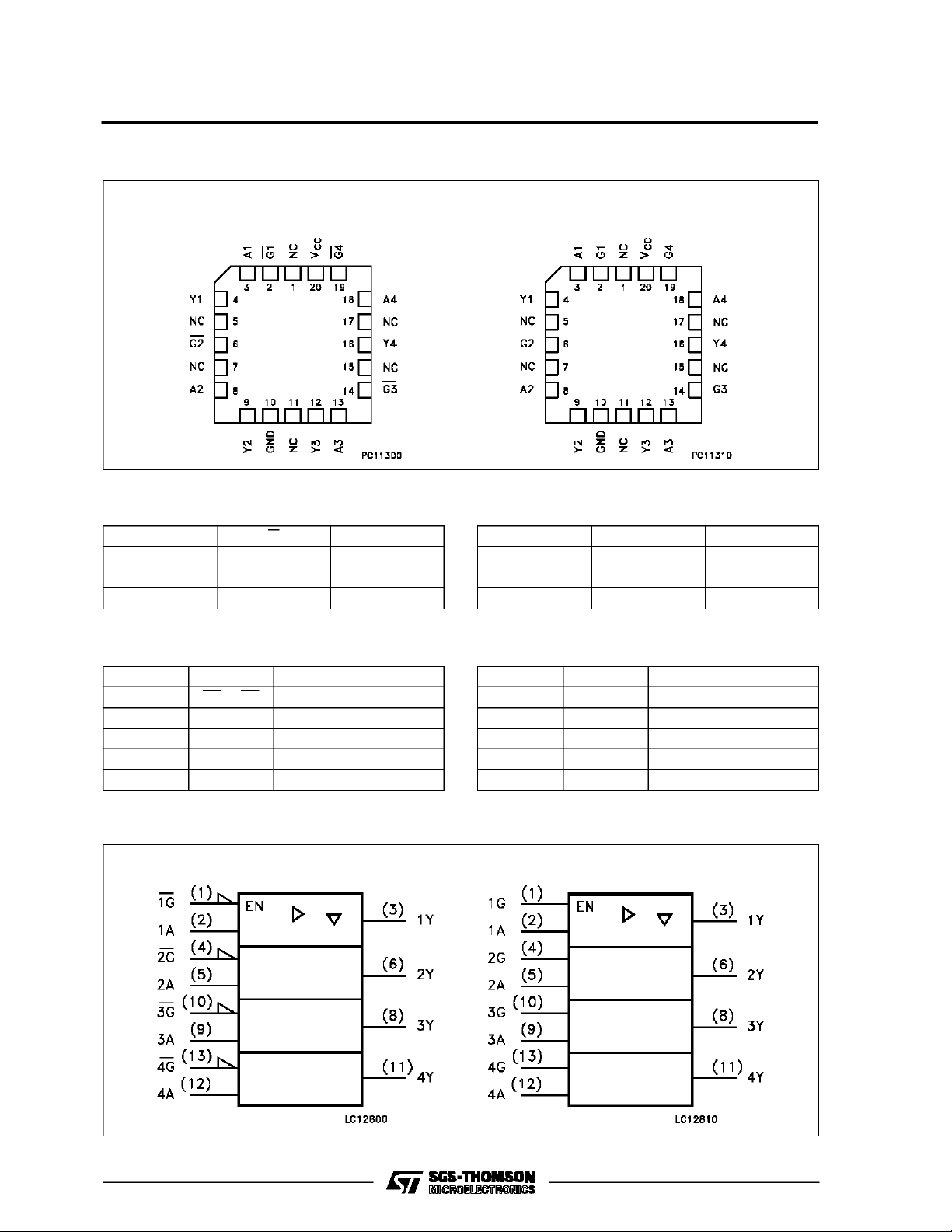
M54/M74HC125/126
CHIP CARRIER
HC125 HC126
TRUTH TABLE (HC125)
AGY
XHZ
LLL
HLH
PIN DESCRIPTION (HC125)
PIN No SYMBOL NAME AND FUNCTION
1, 4, 10, 13 G1 to G4 OutputEnable Input
2, 5, 9, 12 A1 to A4 Data Inputs
3, 6, 8, 11 Y1 to Y4 Data Outputs
7 GND Ground (0V)
14 V
CC
Positive Supply Voltage
IEC LOGIC SYMBOLS
HC125 HC126
TRUTH TABLE (HC126)
AGY
XLZ
LHL
HHH
PIN DESCRIPTIO N (HC1 26)
PIN No SYMBOL NAME AND FUNCTION
1, 4, 10, 13 G1 to G4 Output Enable Input
2, 5, 9, 12 A1 to A4 Data Inputs
3, 6, 8, 11 Y1 to Y4 Data Outputs
7 GND Ground (0V)
14 V
CC
Positive Supply Voltage
2/11
CIR CUI T DI A GR AM
HC125 HC126
ABSOLU TE M AXIMU M R AT INGS
M54/M74HC125/126
Symbol Parameter Value Unit
V
CC
V
V
O
I
IK
I
OK
I
O
I
or I
CC
P
D
T
stg
T
L
AbsoluteMaximumRatingsarethose values beyond whichdamage tothedevicemayoccur.Functional operationunder theseconditionisnotimplied.
(*)500 mW:≅ 65oC derateto 300 mW by 10mW/oC: 65oCto85oC
Supply Voltage -0.5 to +7 V
DC Input Voltage -0.5 to VCC+ 0.5 V
I
DC Output Voltage -0.5 to VCC+ 0.5 V
DC Input Diode Current ± 20 mA
DC Output Diode Current ± 20 mA
DC Output Source Sink Current Per Output Pin ± 35 mA
DC VCCor Ground Current ± 70 mA
GND
Power Dissipation 500 (*) mW
Storage Temperature -65 to +150
Lead Temperature (10 sec) 300
o
C
o
C
RECO MM ENDED OPERAT I N G CO NDI TIONS
Symbol Parameter Value Unit
V
V
T
t
V
r,tf
Supply Voltage 2 to 6 V
CC
Input Voltage 0 to V
I
Output Voltage 0 to V
O
Operating Temperature: M54HC Series
op
M74HC Series
CC
CC
-55 to +125
-40 to +85
Input Rise and Fall Time VCC= 2 V 0 to 1000 ns
V
= 4.5 V 0 to 500
CC
V
= 6 V 0 to 400
CC
V
V
o
C
o
C
3/11
M54/M74HC125/126
DC SPECIFICATIONS
Symbol Parameter
V
V
V
V
I
I
High Level Input
IH
Voltage
Low Level Input
IL
Voltage
High Level
OH
Output Voltage
Low Level Output
OL
Voltage
I
Input Leakage
I
Current
3 State Output
OZ
Off-state Current
Quiescent Supply
CC
Current
Test Conditions Value
V
(V)
CC
=25oC
A
54HC and 74HC
Min. Typ. Max. Min. Max. Min. Max.
-40 to 85oC
74HC
-55 to 125oC
54HC
Unit
T
2.0 1.5 1.5 1.5
4.5 3.15 3.15 3.15
6.0 4.2 4.2 4.2
2.0 0.5 0.5 0.5
4.5 1.35 1.35 1.35
6.0 1.8 1.8 1.8
2.0
4.5 4.4 4.5 4.4 4.4
6.0 5.9 6.0 5.9 5.9
4.5 I
6.0 I
2.0
4.5 0.0 0.1 0.1 0.1
6.0 0.0 0.1 0.1 0.1
4.5 I
6.0 I
6.0
6.0
=
V
I
IO=-20 µA
V
IH
or
V
IL
=-6.0 mA 4.18 4.31 4.13 4.10
O
=-7.8 mA 5.68 5.8 5.63 5.60
O
V
=
I
IO=20µA
V
IH
or
V
IL
= 6.0 mA 0.17 0.26 0.33 0.40
O
= 7.8 mA 0.18 0.26 0.33 0.40
O
VI=VCCor GND ±0.1 ±1 ±1 µA
V
I=VIH
or V
VO=VCCor GND
1.9 2.0 1.9 1.9
0.0 0.1 0.1 0.1
IL
±0.5 ±5 ±10 µA
6.0 VI=VCCor GND 4 40 80 µA
V
V
V
V
4/11

M54/M74HC125/126
AC ELECTRICAL CHARACTERISTICS (Inp ut tr=tf=6ns)
Test Conditions Value
T
=25oC
Symbol Parameter
t
t
TLH
THL
Output Transition
Time
V
C
CC
(V)
L
(pF)
2.0
50
4.5 6121518
A
54HC and 74HC
Min. Typ. Max. Min. Max. Min. Max.
20 60 75 90
6.0 5101315
t
PLH
t
PHL
Propagation
Delay Time
2.0
50
4.5 9151922
36 75 95 110
6.0 8131619
2.0
150
4.5 13 21 26 32
52 105 130 160
6.0 11 18 22 27
t
t
PZL
PZH
3 State Output
Enable Time
2.0
50 RL=1KΩ
4.5 9151922
36 75 95 110
6.0 8131619
2.0
150 R
4.5 13 21 26 32
=1KΩ
L
52 105 130 160
6.0 11 18 22 27
t
t
PLZ
PHZ
3 State Output
Disable Time
2.0
50 R
4.5 12 16 20 24
=1KΩ
L
48 80 100 120
6.0 10 14 17 20
C
C
PD
Input Capacitance 5 10 10 10 pF
IN
(*) Power Dissipation
35
Capacitance
(*) CPDisdefined as the valueof the IC’s internal equivalent capacitance which is calculated fromthe operating current consumption withoutload.
(Referto Test Circuit). Average operting currentcan be obtained bythe followingequation. ICC(opr) = CPD•VCC•fIN+I
-40 to 85oC
74HC
-55 to 125oC
54HC
CC
Unit
ns
ns
ns
ns
ns
ns
pF
SWITCHING CHARACTERISTICS TEST WAVEFORM
HC125
A
Y
HC126
A
Y
G
Y
G
Y
5/11

M54/M74HC125/126
TEST CIRCUIT ICC(Opr.)
HC125
THE OTHER INPUTS ARE CONNECTED TO V
HC126
THE OTHER INPUTS ARE CONNECTED TO V
LINEOR GND LINE
CC
LINEOR GND LINE
CC
6/11

Plastic DIP14 MECHANICAL DATA
M54/M74HC125/126
DIM.
MIN. TYP. MAX. MIN. TYP. MAX.
a1 0.51 0.020
B 1.39 1.65 0.055 0.065
b 0.5 0.020
b1 0.25 0.010
D 20 0.787
E 8.5 0.335
e 2.54 0.100
e3 15.24 0.600
F 7.1 0.280
I 5.1 0.201
L 3.3 0.130
Z 1.27 2.54 0.050 0.100
mm inch
P001A
7/11

M54/M74HC125/126
Ceramic DIP14/1 MECHANICAL DATA
DIM.
MIN. TYP. MAX. MIN. TYP. MAX.
A 20 0.787
B 7.0 0.276
D 3.3 0.130
E 0.38 0.015
e3 15.24 0.600
F 2.29 2.79 0.090 0.110
G 0.4 0.55 0.016 0.022
H 1.17 1.52 0.046 0.060
L 0.22 0.31 0.009 0.012
M 1.52 2.54 0.060 0.100
N 10.3 0.406
P 7.8 8.05 0.307 0.317
Q 5.08 0.200
mm inch
8/11
P053C

SO14 MECHANICAL DATA
M54/M74HC125/126
DIM.
MIN. TYP. MAX. MIN. TYP. MAX.
A 1.75 0.068
a1 0.1 0.2 0.003 0.007
a2 1.65 0.064
b 0.35 0.46 0.013 0.018
b1 0.19 0.25 0.007 0.010
C 0.5 0.019
c1 45° (typ.)
D 8.55 8.75 0.336 0.344
E 5.8 6.2 0.228 0.244
e 1.27 0.050
e3 7.62 0.300
F 3.8 4.0 0.149 0.157
G 4.6 5.3 0.181 0.208
L 0.5 1.27 0.019 0.050
M 0.68 0.026
S8°(max.)
mm inch
P013G
9/11

M54/M74HC125/126
PLCC20 MECHANICAL DATA
DIM.
MIN. TYP. MAX. MIN. TYP. MAX.
A 9.78 10.03 0.385 0.395
B 8.89 9.04 0.350 0.356
D 4.2 4.57 0.165 0.180
d1 2.54 0.100
d2 0.56 0.022
E 7.37 8.38 0.290 0.330
e 1.27 0.050
e3 5.08 0.200
F 0.38 0.015
G 0.101 0.004
M 1.27 0.050
M1 1.14 0.045
mm inch
10/11
P027A

M54/M74HC125/126
Information furnished is believed to be accurate and reliable.However, SGS-THOMSON Microelectronics assumes no responsability for the
consequences of use of such information nor for any infringement of patents or other rights of third parties which may results from its use. No
license is granted byimplication or otherwise under any patent or patentrights of SGS-THOMSON Microelectronics. Specificationsmentioned
in this publication are subject to change without notice. This publication supersedes and replaces all information previously supplied.
SGS-THOMSON Microelectronicsproducts are not authorized foruse ascritical componentsin life support devices orsystems without express
written approval of SGS-THOMSON Microelectonics.
1994 SGS-THOMSON Microelectronics - All Rights Reserved
Australia - Brazil - France - Germany - Hong Kong - Italy - Japan - Korea - Malaysia - Malta - Morocco - The Netherlands -
Singapore -Spain - Sweden - Switzerland - Taiwan - Thailand - United Kingdom - U.S.A
SGS-THOMSON Microelectronics GROUP OF COMPANIES
11/11
 Loading...