

M74HC03
QUAD 2-INPUT OPEN DRAIN NAND GATE
■ HIGH SPEED:
t
= 8ns (TYP.) at VCC = 6V
PD
■ LOW POWER DISSIPATION:
I
= 1µA(MAX.) at TA=25°C
CC
■ HIGH NOISE IMMUNITY:
V
= V
NIH
■ BALANCED PROPAGATION DELAYS:
t
≅ t
PLH
■ WIDE OPERATING VOLTAGE RANGE:
V
(OPR) = 2V to 6V
CC
■ PIN AND FUNCTION COMPATIBLE WITH
= 28 % VCC (MIN.)
NIL
PHL
74 SERIES 03
DESCRIPTION
The M74HC03 is an high speed CMOS QUAD
2-INPUT OPEN DRAIN NAND GATE fabricated
with silicon gate C
2
MOS technology.
The internal circuit is composed of 3 stages
including buffer output , which enables high noise
immunity and stable output. This device can, with
an external pull-up resistor, be used in wired AND
configuration. This device can be al so used as a
TSSOPDIP SOP
ORDER CODES
PACKAGE TUBE T & R
DIP M74HC03B1R
SOP M74HC03M1R M74HC03RM13TR
TSSOP M74HC03TTR
led driver and in any other application requ iring a
current sink.
All inputs are equipped with protection circuits
against static discharge and transient excess
voltage.
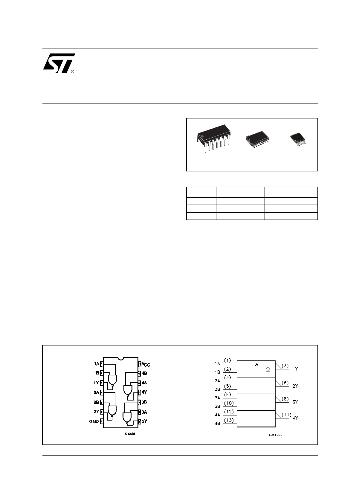
PIN CONNECTION AND IEC LOGIC SYMBOLS
1/8July 2001
M74HC03
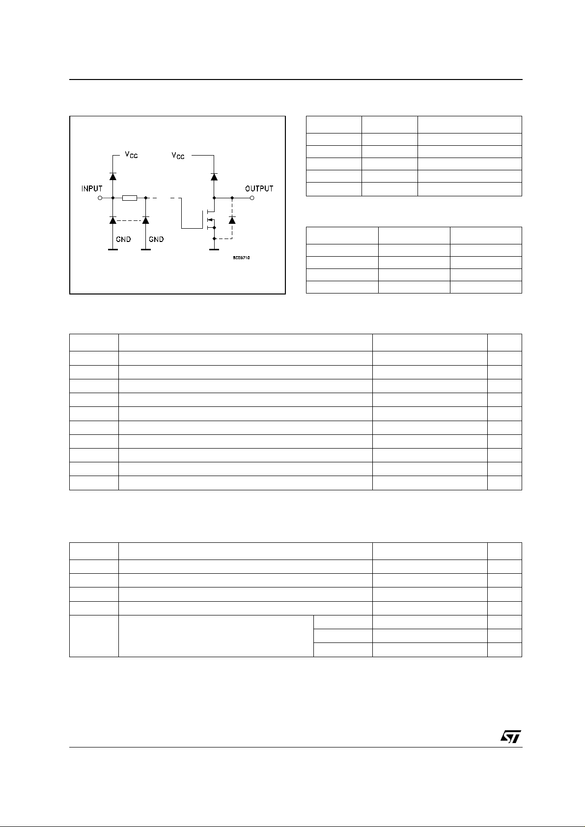
INPUT AND OUTPUT EQUIVALENT CIRCUIT PIN DESCRIPTION
PIN No SYMBOL NAME AND FUNCTION
1, 4, 9, 12 1A to 4A Data Inputs
2, 5, 10, 13 1B to 4B Data Inputs
3, 6, 8, 11 1Y to 4Y Data Outputs
7 GND Ground (0V)
14
V
CC
TRUTH TABLE
ABY
LLZ
LHZ
HLZ
HHL
Z : High Impedance
ABSOLUTE MAXIMUM RATINGS
Symbol Parameter Value Unit
V
V
V
I
I
OK
I
I
or I
CC
P
T
T
Absolute Maximum Ratings are those values beyond which damage to the device may occur. Functional operation under these conditions is
not implied
(*) 500mW at 65
Supply Voltage
CC
DC Input Voltage -0.5 to VCC + 0.5
I
DC Output Voltage -0.5 to VCC + 0.5
O
DC Input Diode Current
IK
DC Output Diode Current
DC Output Current
O
DC VCC or Ground Current
GND
Power Dissipation
D
Storage Temperature
stg
Lead Temperature (10 sec)
L
°C; derate to 300mW by 10mW/°C from 65°C to 85°C
Positive Supply Voltage
-0.5 to +7 V
V
V
± 20 mA
± 20 mA
+ 25 mA
± 50 mA
500(*) mW
-65 to +150 °C
300 °C
RECOMMENDED OPERATING CONDITIONS
Symbol Parameter Value Unit
2/8
V
V
V
T
t
r
Supply Voltage
CC
Input Voltage 0 to V
I
Output Voltage 0 to V
O
Operating Temperature
op
Input Rise and Fall Time VCC = 2.0V
, t
f
V
V
CC
CC
= 4.5V
= 6.0V
2 to 6 V
CC
CC
-55 to 125 °C
0 to 1000 ns
0 to 500 ns
0 to 400 ns
V
V
DC SPECIFICATIONS
Symbol Parameter
V
V
V
I
I
High Level Input
IH
Voltage
Low Level Input
IL
Voltage
Low Level Output
OL
Voltage
I
Input Leakage
I
Current
Output Leakage
OZ
Current
Quiescent Supply
CC
Current
M74HC03
Test Condition Value
T
= 25°C
V
CC
(V)
A
Min. Typ. Max. Min. Max. Min. Max.
2.0 1.5 1.5 1.5
6.0 4.2 4.2 4.2
2.0 0.5 0.5 0.5
6.0 1.8 1.8 1.8
2.0
4.5
6.0
4.5
6.0
6.0
6.0
6.0
IO=20 µA
I
=20 µA
O
I
=20 µA
O
I
=4.0 mA
O
I
=5.2 mA
O
= VCC or GND
V
I
VI = VIH or V
IL
VO = VCC or GND
= VCC or GND
V
I
0.0 0.1 0.1 0.1
0.0 0.1 0.1 0.1
0.0 0.1 0.1 0.1
0.17 0.26 0.33 0.40
0.18 0.26 0.33 0.40
-40 to 85°C -55 to 125°C
± 0.1 ± 1 ± 1 µA
±0.5 ± 5 ± 10 µA
11020µA
Unit
V4.5 3.15 3.15 3.15
V4.5 1.35 1.35 1.35
V
AC ELECTRICAL CHARACTERISTICS (C
Test Condition Value
Symbol Parameter
V
CC
(V)
t
Output Transition
THL
Time
2.0 30 75 95 110
6.0 7131619
t
Propagation Delay
PLZ
Time
2.0
R
= 1 KΩ
L
6.0 8101315
t
Propagation Delay
PZL
Time
2.0
R
= 1 KΩ
L
6.0 6101315
CAPACITIVE CHARACTERISTICS
Test Condition Value
Symbol Parameter
C
C
Input Capacitance
IN
Power Dissipation
PD
Capacitance (note 1)5.0 7 pF
V
CC
(V)
5.0 5101010pF
= 50 pF, Input tr = tf = 6ns)
L
= 25°C
T
A
Min. Typ. Max. Min. Max. Min. Max.
16 60 75 90
23 60 75 90
= 25°C
T
A
Min. Typ. Max. Min. Max. Min. Max.
-40 to 85°C -55 to 125°C
-40 to 85°C -55 to 125°C
Unit
ns4.5 8151922
ns4.5 9121518
ns4.5 7121518
Unit
1) CPD is defined as the value of the IC’s internal equivalent capacitance which is calculated from the operating current consumption without
load. (Refer to Test Circuit). Average operating current can be obtained by the following equation. I
= CPD x VCC x fIN + ICC/4 (per gate)
CC(opr)
3/8
 Loading...