

QUAD 2-INPUT OPEN DRAIN NAND GATE
.HIGH SPEED
tPZ= 5 ns (TYP.) AT VCC=5V
.LOWPOWER DISSIPATION
ICC=1µA(MAX.) AT TA=25°C
.HIGH NOISE IMMUNITY
V
NIH=VNIL
=28%VCC(MIN.)
.OUTPUT DRIVE CAPABILITY
10 LSTTLLOADS
.BALANCEDPROPAGATION DELAYS
t
PLH=tPHL
.WIDE OPERATING VOLTAGE RANGE
VCC(OPR)= 2 V TO 6 V
.PIN AND FUNCTION COMPATIBLE WITH
54/74LS03
M54HC03
M74HC03
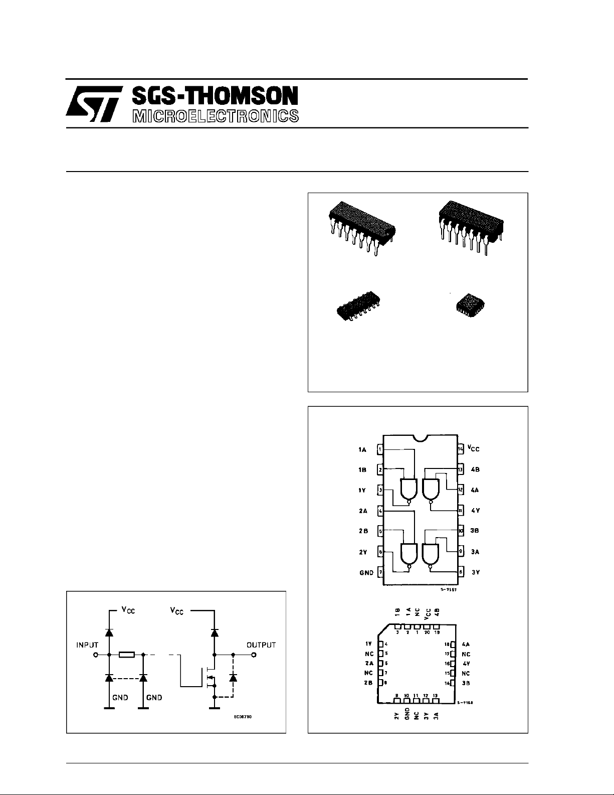
B1R
(PlasticPackage)
M1R
(MicroPackage)
ORDER CODES :
M54HC 03F1R M74H C03M1R
M74HC 03B1R M74HC0 3C1R
(CeramicPackage)
(Chip Carrier)
F1R
C1R
DESCRIPTION
The M54/74HC03 is a high speedCMOS QUAD2INPUTOPENDRAINNANDGATEfabricated insilicon gate C2MOS technology.
It has the same high speed performance of LSTTL
combined withtrue CMOSlow power consumption.
The internal circuitis composedof 3 stages including buffer output, which gives high noise immunity
and stableoutput. This device can, with an external
pull-up resistor,beusedinwiredANDconfiguration.
This device can be also used as a led driver and in
any other application requiring acurrentsink. All inputs are equipped with protection circuits against
staticdischarge and transient excessvoltage.
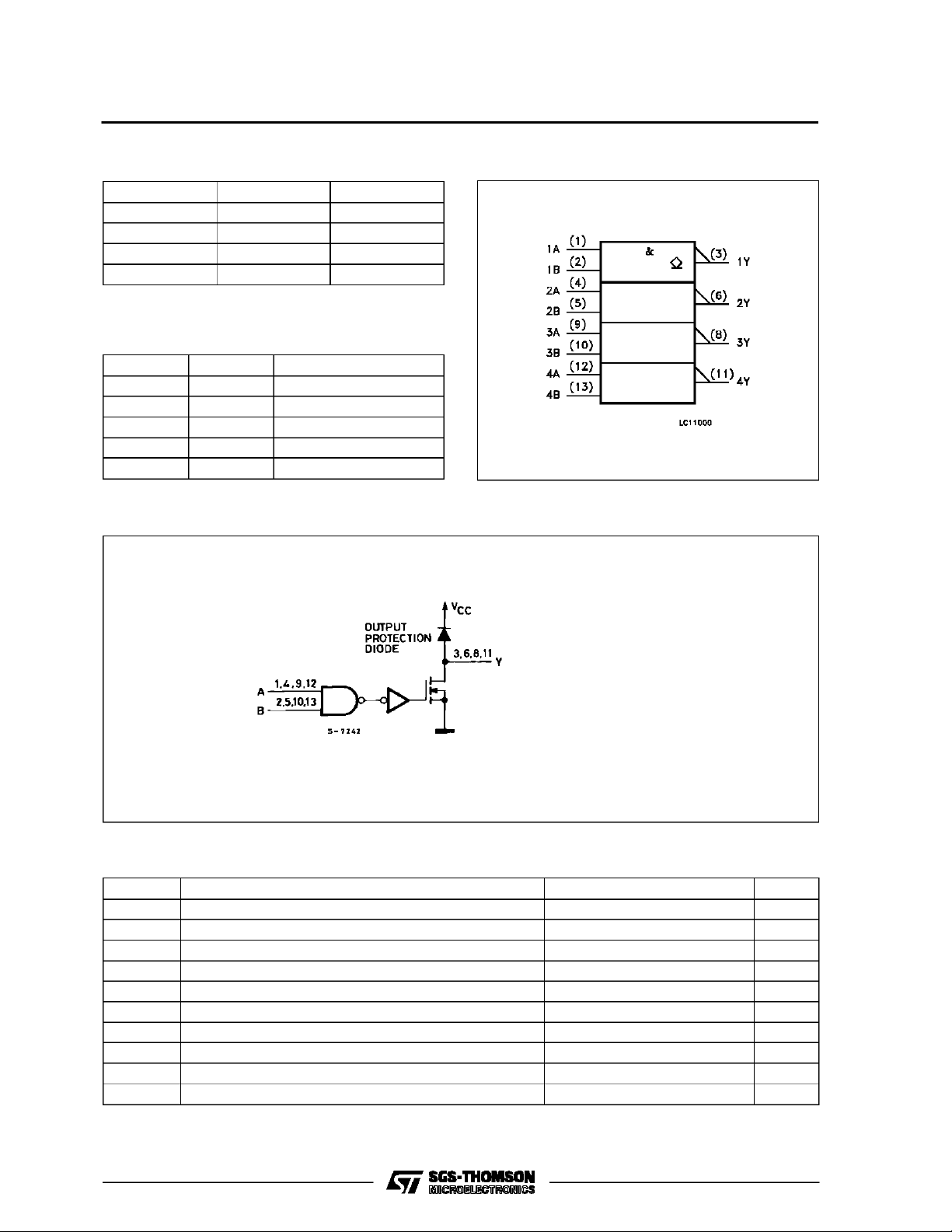
INPUT AND OUTPUT EQUIVALENT CIRCUIT
PIN CONNECTIONS(top view)
January 1993
NC =
No Internal
Connection
1/9
M54/M74HC03
TRUTH TABLE
ABY
LLZ
LHZ
HLZ
HHL
Z =HIGHIMPEDANCE
PIN DESCRIPTION
PIN No SYMBOL NAME AND FUNCTION
1, 4, 9, 12 1A to 4A Data Inputs
2, 5, 10, 13 1B to 4B Data Inputs
3, 6, 8, 11 1Y to 4Y Data Outputs
7 GND Ground (0V)
14 V
CC
Positive Supply Voltage
CIR CUI T DIA GR AM
IEC LOGIC SYMBOL
VCC= Pin14
GND = Pin 7
open–drain outputs
ABSOLU TE MAXIMU M RAT INGS
Symbol Parameter Value Unit
V
CC
V
V
O
I
IK
I
OK
I
O
I
or I
CC
P
D
T
stg
T
L
AbsoluteMaximumRatingsarethosevaluesbeyondwhichdamage tothedevicemayoccur. Functionaloperationunder theseconditionisnotimplied.
(*)500 mW: ≅ 65oC derateto300 mWby 10mW/oC: 65oCto85oC
Supply Voltage -0.5 to +7 V
DC Input Voltage -0.5 to VCC+ 0.5 V
I
DC Output Voltage -0.5 to VCC+ 0.5 V
DC Input Diode Current ± 20 mA
DC Output Diode Current ± 20 mA
DC Output Sink Current Per Output Pin + 25 mA
DC VCCor Ground Current ± 50 mA
GND
Power Dissipation 500 (*) mW
Storage Temperature -65 to +150
Lead Temperature (10 sec) 300
o
C
o
C
2/9
M54/M74HC03
RECO MM ENDED OPERATI N G C ONDI TIONS
Symbol Parameter Value Unit
V
V
V
T
t
r,tf
DC SPECIF ICATIO NS
Symbol Parameter
V
IH
V
V
OL
I
I
OZ
I
CC
Supply Voltage 2 to 6 V
CC
Input Voltage 0 to V
I
Output Voltage 0 to V
O
Operating Temperature: M54HC Series
op
M74HC Series
CC
CC
-55 to +125
-40 to +85
Input Rise and Fall Time VCC= 2 V 0 to 1000 ns
V
= 4.5 V 0 to 500
CC
V
= 6 V 0 to 400
CC
Test Conditions Value
V
(V)
CC
=25oC
T
A
54HC and 74HC
-40 to 85oC
74HC
-55 to 125oC
Min. Typ. Max. Min. Max. Min. Max.
High Level Input
Voltage
2.0 1.5 1.5 1.5
4.5 3.15 3.15 3.15
6.0 4.2 4.2 4.2
Low Level Input
IL
Voltage
2.0 0.5 0.5 0.5
4.5 1.35 1.35 1.35
6.0 1.8 1.8 1.8
Low Level Output
Voltage
Input Leakage
I
Current
Output Leakage
Current
Quiescent Supply
2.0
V
=
I
4.5 0.0 0.1 0.1 0.1
6.0 0.0 0.1 0.1 0.1
4.5 I
6.0 I
6.0
6.0
IO=20µA
V
IH
or
V
IL
= 4.0 mA 0.17 0.26 0.33 0.40
O
= 5.2 mA 0.18 0.26 0.33 0.40
O
VI=VCCor GND ±0.1 ±1 ±1 µA
VI=VIHor V
IL
VO=VCCor GND
0.0 0.1 0.1 0.1
±0.5 ±5 ±10 µA
6.0 VI=VCCor GND 1 10 20 µA
Current
54HC
V
V
o
C
o
C
Unit
V
V
V
3/9

M54/M74HC03
AC ELECTRICAL CHARACTERISTICS (CL=50pF,Inputtr=tf=6ns)
Test Conditions Value
T
=25oC
Symbol Parameter
t
t
TLH
THL
Output Transition
Time
V
CC
(V)
2.0 30 75 95 110
4.5 8151922
A
54HC and 74HC
Min. Typ. Max. Min. Max. Min. Max.
6.0 7131619
t
PLZ
Propagation
Delay Time
2.0
RL = 1 KΩ
4.5 9121518
16 60 75 90
6.0 8101315
t
PZL
Propagation
Delay Time
2.0
RL=1KΩ
4.5 7121518
23 60 75 90
6.0 6101315
C
C
PD
Input Capacitance 5 10 10 10 pF
IN
(*) Power Dissipation
7
Capacitance
(*) CPDisdefined as the valueof the IC’s internal equivalent capacitance which is calculatedfromthe operatingcurrent consumption without load.
(Referto Test Circuit).Average operting current can be obtained bythefollowingequation. ICC(opr) = CPD•VCC•fIN+ICC/4(per Gate)
-40 to 85oC
74HC
-55 to 125oC
54HC
Unit
ns
ns
ns
pF
TYPICAL APPLICATIONS
WiredAND LEDDriver with Blanking
W = Y1 Y2 ...Yn = A1B1 A2B2...AnBn= A1B1 + A2B2+...+ AnBn
ID=10:20mA
V
−
V
−
V
CC
R
=
D
(*)260Ω with ID=10mA
D
I
D
DS
=
5 − 2 − 0.4
−3
20 × 10
= 130 Ω (*)
Typicalvalues
VCC=5V
VD=2V
VDS=0.4V
RD= 120 ÷ 270Ω
4/9

Plastic DIP14 MECHANICAL DATA
M54/M74HC03
DIM.
MIN. TYP. MAX. MIN. TYP. MAX.
a1 0.51 0.020
B 1.39 1.65 0.055 0.065
b 0.5 0.020
b1 0.25 0.010
D 20 0.787
E 8.5 0.335
e 2.54 0.100
e3 15.24 0.600
F 7.1 0.280
I 5.1 0.201
L 3.3 0.130
Z 1.27 2.54 0.050 0.100
mm inch
P001A
5/9

M54/M74HC03
Ceramic DIP14/1 MECHANICAL DATA
DIM.
MIN. TYP. MAX. MIN. TYP. MAX.
A 20 0.787
B 7.0 0.276
D 3.3 0.130
E 0.38 0.015
e3 15.24 0.600
F 2.29 2.79 0.090 0.110
G 0.4 0.55 0.016 0.022
H 1.17 1.52 0.046 0.060
L 0.22 0.31 0.009 0.012
M 1.52 2.54 0.060 0.100
N 10.3 0.406
P 7.8 8.05 0.307 0.317
Q 5.08 0.200
mm inch
6/9
P053C

SO14 MECHANICAL DATA
M54/M74HC03
DIM.
MIN. TYP. MAX. MIN. TYP. MAX.
A 1.75 0.068
a1 0.1 0.2 0.003 0.007
a2 1.65 0.064
b 0.35 0.46 0.013 0.018
b1 0.19 0.25 0.007 0.010
C 0.5 0.019
c1 45° (typ.)
D 8.55 8.75 0.336 0.344
E 5.8 6.2 0.228 0.244
e 1.27 0.050
e3 7.62 0.300
F 3.8 4.0 0.149 0.157
G 4.6 5.3 0.181 0.208
L 0.5 1.27 0.019 0.050
M 0.68 0.026
S8°(max.)
mm inch
P013G
7/9

M54/M74HC03
PLCC20 MECHANICAL DATA
DIM.
MIN. TYP. MAX. MIN. TYP. MAX.
A 9.78 10.03 0.385 0.395
B 8.89 9.04 0.350 0.356
D 4.2 4.57 0.165 0.180
d1 2.54 0.100
d2 0.56 0.022
E 7.37 8.38 0.290 0.330
e 1.27 0.050
e3 5.08 0.200
F 0.38 0.015
G 0.101 0.004
M 1.27 0.050
M1 1.14 0.045
mm inch
8/9
P027A

M54/M74HC03
Information furnished is believed to be accurate and reliable. However, SGS-THOMSON Microelectronics assumes no responsability for the
consequences of use of such information nor for any infringement of patents or other rights of third parties which may results from its use. No
license is granted byimplication or otherwise under any patent or patentrights of SGS-THOMSON Microelectronics. Specificationsmentioned
in this publication are subject to change without notice. This publication supersedes and replaces all information previously supplied.
SGS-THOMSON Microelectronicsproducts are not authorized foruse ascritical componentsin life support devices or systems without express
written approval of SGS-THOMSON Microelectonics.
1994 SGS-THOMSON Microelectronics - All Rights Reserved
Australia - Brazil - France - Germany - Hong Kong - Italy - Japan - Korea - Malaysia - Malta - Morocco - The Netherlands -
Singapore -Spain - Sweden- Switzerland -Taiwan - Thailand - United Kingdom - U.S.A
SGS-THOMSON Microelectronics GROUP OF COMPANIES
9/9
 Loading...