

1/150
PRELIMINARY DATA
December 2001
This is preliminary information on a new product now in development or undergoing evaluation. Details are subject to change without notice.
M7020R
32K x 68-bit Entry NETWORK SEARCH ENGINE
FEATURES SUMMARY
■ 32K DATA ENTRIES IN 68-BIT MODE
■ TABLE MAY BE PARTITIONED INTO UP TO
FOUR (4) QUADRANTS
(Data entry width in each oc tant is conf igurab le
as 34, 68, 136, or 272 bits.)
■ UP TO 83 MILLION SUSTAINED SEARCHES
PER SECOND IN 68-BIT and 136-BIT
CONFIGURATIONS
■ UP TO 41.5 MILLION SEARCHES PER
SECOND IN 34-BIT and 272-BIT
CONFIGURATIONS
■ SEARCHES ANY SUB-FIELD IN A SINGLE
CYCLE
■ OFFERS BIT-BY-BIT and GLOBAL MASKING
■ SYNCHRONOUS, PIPELINED OPERATION
■ UP TO 31 SEARCH ENGINES CASCADABLE
WITHOUT PERFORMANCE DEGRADATION
■ WHEN CASCADED, THE DATABASE
ENTRIES CAN SCALE FROM 248K TO 1984K
DEPENDING ON THE WIDTH OF THE ENTRY
■ GLUELESS INTERFACE TO INDUSTRY-
STANDARD SRAMS
■ SIMPLE HARDWARE INSTRUCTION
INTERFACE
■ IEEE 1149.1 TEST ACCESS PORT
■ OPER A T I NG SUPPLY VOLTAGES INCLUD E:
V
DD
(Operating Supply Voltage) = 1.8V
V
DDQ
(Operating Supply Voltage for I/O) = 2.5
or 3.3V
■ 272 PBGA, 27mm x 27mm
Figure 1. 272-ball PBGA Package
272-ball PBGA
27mm x 27mm

M7020R
2/150
TABLE OF CONTENTS
DESCRIPTION . . . . . . . . . . . . . . . . . . . . . . . . . . . . . . . . . . . . . . . . . . . . . . . . . . . . . . . . . . . . . . . . . . . . 8
Overview . . . . . . . . . . . . . . . . . . . . . . . . . . . . . . . . . . . . . . . . . . . . . . . . . . . . . . . . . . . . . . . . . . . . . . 8
Performance . . . . . . . . . . . . . . . . . . . . . . . . . . . . . . . . . . . . . . . . . . . . . . . . . . . . . . . . . . . . . . . . . . . 8
Applications. . . . . . . . . . . . . . . . . . . . . . . . . . . . . . . . . . . . . . . . . . . . . . . . . . . . . . . . . . . . . . . . . . . . 8
Product Range (Table 1.) . . . . . . . . . . . . . . . . . . . . . . . . . . . . . . . . . . . . . . . . . . . . . . . . . . . . . . . . . 8
Switch/Router Implementation Using the M7020R (Figure 2.) . . . . . . . . . . . . . . . . . . . . . . . . . . . . . 8
Signal Names (Table 2.) . . . . . . . . . . . . . . . . . . . . . . . . . . . . . . . . . . . . . . . . . . . . . . . . . . . . . . . . . . 9
Connections (Figure 3.). . . . . . . . . . . . . . . . . . . . . . . . . . . . . . . . . . . . . . . . . . . . . . . . . . . . . . . . . . 1 0
M7020R Block Diagram (Figure 4.). . . . . . . . . . . . . . . . . . . . . . . . . . . . . . . . . . . . . . . . . . . . . . . . .11
MAXIMUM RATING. . . . . . . . . . . . . . . . . . . . . . . . . . . . . . . . . . . . . . . . . . . . . . . . . . . . . . . . . . . . . . . . 12
Absolute Maximum Ratings (Table 3.) . . . . . . . . . . . . . . . . . . . . . . . . . . . . . . . . . . . . . . . . . . . . . . 12
DC AND AC PARAMETERS. . . . . . . . . . . . . . . . . . . . . . . . . . . . . . . . . . . . . . . . . . . . . . . . . . . . . . . . . 13
DC and AC Measurement Conditions (Table 4.). . . . . . . . . . . . . . . . . . . . . . . . . . . . . . . . . . . . . . . 13
M7020R 2.5, or 3.3V AC Testing Load (Figure 5.) . . . . . . . . . . . . . . . . . . . . . . . . . . . . . . . . . . . . . 14
M7020R 2.5, or 3.3V Input Waveform (Figure 6.) . . . . . . . . . . . . . . . . . . . . . . . . . . . . . . . . . . . . . . 14
M7020R 2.5, or 3.3V I/O Output Load Equivalent (Figure 7.) . . . . . . . . . . . . . . . . . . . . . . . . . . . . . 14
Capacitance (Table 5.) . . . . . . . . . . . . . . . . . . . . . . . . . . . . . . . . . . . . . . . . . . . . . . . . . . . . . . . . . . 15
DC Characteristics (Table 6.) . . . . . . . . . . . . . . . . . . . . . . . . . . . . . . . . . . . . . . . . . . . . . . . . . . . . . 1 5
AC Timing Waveforms with CLK2X (Figure 8.). . . . . . . . . . . . . . . . . . . . . . . . . . . . . . . . . . . . . . . . 16
AC Timing Parameters with CLK2X (Table 7.) . . . . . . . . . . . . . . . . . . . . . . . . . . . . . . . . . . . . . . . .17
OPERATION . . . . . . . . . . . . . . . . . . . . . . . . . . . . . . . . . . . . . . . . . . . . . . . . . . . . . . . . . . . . . . . . . . . . . 18
CMD Bus and DQ Bus. . . . . . . . . . . . . . . . . . . . . . . . . . . . . . . . . . . . . . . . . . . . . . . . . . . . . . . . . . . 18
Database Entry (Data Array and Mask Array). . . . . . . . . . . . . . . . . . . . . . . . . . . . . . . . . . . . . . . . . 18
Arbitration Logic . . . . . . . . . . . . . . . . . . . . . . . . . . . . . . . . . . . . . . . . . . . . . . . . . . . . . . . . . . . . . . . . 18
Pipeline and SRAM Control . . . . . . . . . . . . . . . . . . . . . . . . . . . . . . . . . . . . . . . . . . . . . . . . . . . . . . . 18
Full Logic. . . . . . . . . . . . . . . . . . . . . . . . . . . . . . . . . . . . . . . . . . . . . . . . . . . . . . . . . . . . . . . . . . . . . 18
CONNECTION DESCRIPTIONS. . . . . . . . . . . . . . . . . . . . . . . . . . . . . . . . . . . . . . . . . . . . . . . . . . . . . . 19
Clocks and Reset . . . . . . . . . . . . . . . . . . . . . . . . . . . . . . . . . . . . . . . . . . . . . . . . . . . . . . . . . . . . . . 19
CMD and DQ Bus . . . . . . . . . . . . . . . . . . . . . . . . . . . . . . . . . . . . . . . . . . . . . . . . . . . . . . . . . . . . . . 19
SRAM Interface. . . . . . . . . . . . . . . . . . . . . . . . . . . . . . . . . . . . . . . . . . . . . . . . . . . . . . . . . . . . . . . . 19
Cascade Interface . . . . . . . . . . . . . . . . . . . . . . . . . . . . . . . . . . . . . . . . . . . . . . . . . . . . . . . . . . . . . . 19
Device Identification . . . . . . . . . . . . . . . . . . . . . . . . . . . . . . . . . . . . . . . . . . . . . . . . . . . . . . . . . . . . 20
Supplies. . . . . . . . . . . . . . . . . . . . . . . . . . . . . . . . . . . . . . . . . . . . . . . . . . . . . . . . . . . . . . . . . . . . . . 20
Test Access Port . . . . . . . . . . . . . . . . . . . . . . . . . . . . . . . . . . . . . . . . . . . . . . . . . . . . . . . . . . . . . . . 20
CLOCKS . . . . . . . . . . . . . . . . . . . . . . . . . . . . . . . . . . . . . . . . . . . . . . . . . . . . . . . . . . . . . . . . . . . . . . . . 20
Clocks (CLK2X and PHS_L) (Figure 9.) . . . . . . . . . . . . . . . . . . . . . . . . . . . . . . . . . . . . . . . . . . . . . 20

3/150
M7020R
REGISTERS . . . . . . . . . . . . . . . . . . . . . . . . . . . . . . . . . . . . . . . . . . . . . . . . . . . . . . . . . . . . . . . . . . . . . 2 1
Register Overview (Table 8.). . . . . . . . . . . . . . . . . . . . . . . . . . . . . . . . . . . . . . . . . . . . . . . . . . . . . . 21
Comparand Registers . . . . . . . . . . . . . . . . . . . . . . . . . . . . . . . . . . . . . . . . . . . . . . . . . . . . . . . . . . . 22
Mask Registers . . . . . . . . . . . . . . . . . . . . . . . . . . . . . . . . . . . . . . . . . . . . . . . . . . . . . . . . . . . . . . . . 22
Comparand Register Selection During SEA RCH and LEARN Instructions (Figure 10.). . . . . . . . . 22
Addressing the Global Masks Register Array (Figure 11.) . . . . . . . . . . . . . . . . . . . . . . . . . . . . . . . 22
SEARCH-Successful Registers (SSR[0:7]). . . . . . . . . . . . . . . . . . . . . . . . . . . . . . . . . . . . . . . . . . . 23
SEARCH-Successful Register (SSR) Description (Table 9.). . . . . . . . . . . . . . . . . . . . . . . . . . . . . . 23
The Command Register . . . . . . . . . . . . . . . . . . . . . . . . . . . . . . . . . . . . . . . . . . . . . . . . . . . . . . . . . 2 4
Command Register Field Descriptions (Table 10.) . . . . . . . . . . . . . . . . . . . . . . . . . . . . . . . . . . . . . 24
The Information Register. . . . . . . . . . . . . . . . . . . . . . . . . . . . . . . . . . . . . . . . . . . . . . . . . . . . . . . . . 25
Information Register Field Descriptions (Table 11.) . . . . . . . . . . . . . . . . . . . . . . . . . . . . . . . . . . . . 25
The Read Burst Address Register (RBURREG) . . . . . . . . . . . . . . . . . . . . . . . . . . . . . . . . . . . . . . . 26
The Write Burst Address Register (WBURREG). . . . . . . . . . . . . . . . . . . . . . . . . . . . . . . . . . . . . . . 26
The NFA Register . . . . . . . . . . . . . . . . . . . . . . . . . . . . . . . . . . . . . . . . . . . . . . . . . . . . . . . . . . . . . . 26
Read Burst Register Description (Table 12.). . . . . . . . . . . . . . . . . . . . . . . . . . . . . . . . . . . . . . . . . . 26
Write Burst Register Description (Table 13.). . . . . . . . . . . . . . . . . . . . . . . . . . . . . . . . . . . . . . . . . . 26
NFA Register (Table 14.). . . . . . . . . . . . . . . . . . . . . . . . . . . . . . . . . . . . . . . . . . . . . . . . . . . . . . . . . 26
SEARCH ENGINE ARCHITECTURE . . . . . . . . . . . . . . . . . . . . . . . . . . . . . . . . . . . . . . . . . . . . . . . . . . 27
Data and Mask Addressing . . . . . . . . . . . . . . . . . . . . . . . . . . . . . . . . . . . . . . . . . . . . . . . . . . . . . . . 2 7
M7020R Database Width Configuration (Figure 12.) . . . . . . . . . . . . . . . . . . . . . . . . . . . . . . . . . . .27
Bit Position Match (Table 15.) . . . . . . . . . . . . . . . . . . . . . . . . . . . . . . . . . . . . . . . . . . . . . . . . . . . . . 28
Multi-width Configuration Example (Figure 13.) . . . . . . . . . . . . . . . . . . . . . . . . . . . . . . . . . . . . . . .28
M7020R Data and Mask Array Addressing (Figure 14.) . . . . . . . . . . . . . . . . . . . . . . . . . . . . . . . . . 28
COMMAND CODES AND PARAMETERS. . . . . . . . . . . . . . . . . . . . . . . . . . . . . . . . . . . . . . . . . . . . . . 29
Command Codes. . . . . . . . . . . . . . . . . . . . . . . . . . . . . . . . . . . . . . . . . . . . . . . . . . . . . . . . . . . . . . . 29
Commands and Command Pa rameters . . . . . . . . . . . . . . . . . . . . . . . . . . . . . . . . . . . . . . . . . . . . . 29
Command Codes (Table 16.) . . . . . . . . . . . . . . . . . . . . . . . . . . . . . . . . . . . . . . . . . . . . . . . . . . . . . 29
Command Parameters (Table 17.) . . . . . . . . . . . . . . . . . . . . . . . . . . . . . . . . . . . . . . . . . . . . . . . . .29
READ COMMAND. . . . . . . . . . . . . . . . . . . . . . . . . . . . . . . . . . . . . . . . . . . . . . . . . . . . . . . . . . . . . . . . . 30
Single Location READ Cycle Timing (Figure 15.) . . . . . . . . . . . . . . . . . . . . . . . . . . . . . . . . . . . . . . 31
Burst READ of the Data and Mask Arrays (BLEN = 4) (Figure 16.) . . . . . . . . . . . . . . . . . . . . . . . . 31
READ Command Parameters (Table 18.). . . . . . . . . . . . . . . . . . . . . . . . . . . . . . . . . . . . . . . . . . . .32
Data and Mask Array, SRAM Read Address Format (Table 19.) . . . . . . . . . . . . . . . . . . . . . . . . . . 32
READ Address Format for Internal Registers (Table 20.). . . . . . . . . . . . . . . . . . . . . . . . . . . . . . . . 33
READ Address Format for Data and Mask Arrays (Table 21.) . . . . . . . . . . . . . . . . . . . . . . . . . . . . 33
WRITE COMMAND. . . . . . . . . . . . . . . . . . . . . . . . . . . . . . . . . . . . . . . . . . . . . . . . . . . . . . . . . . . . . . . . 33
Single Location WRITE Cycle Timing (Figure 17.) . . . . . . . . . . . . . . . . . . . . . . . . . . . . . . . . . . . . . 34
Burst WRITE of the Data and Mask Arrays (BLEN = 4) (Figure 18.). . . . . . . . . . . . . . . . . . . . . . . . 35
(Single) WRITE Address Format for Data and Mask Arrays or SRAM (Table 22.) . . . . . . . . . . . . . 35
WRITE Address Format for Internal Registers (Table 23.) . . . . . . . . . . . . . . . . . . . . . . . . . . . . . . . 36
WRITE Address Format for Data and Mask Array (Burst Write) (Table 24.). . . . . . . . . . . . . . . . . . 36

M7020R
4/150
SEARCH COMMAND . . . . . . . . . . . . . . . . . . . . . . . . . . . . . . . . . . . . . . . . . . . . . . . . . . . . . . . . . . . . . . 36
68-bit Configuration with Single Device . . . . . . . . . . . . . . . . . . . . . . . . . . . . . . . . . . . . . . . . . . . 36
Hardware Diagram for a Table with One Device (Figure 19.). . . . . . . . . . . . . . . . . . . . . . . . . . . . . 37
Timing Diagram for a 68-bit Configuration SEARCH for One Device (Figure 20.) . . . . . . . . . . . . . 38
x68 Table with One Device (Figure 21.) . . . . . . . . . . . . . . . . . . . . . . . . . . . . . . . . . . . . . . . . . . . . .39
Latency of SEARCH from Instruction to SRAM Access Cycle, 68-bit, 1 Device (Table 25.). . . . . . 39
Shift of SSF and SSV from SADR (Table 26.). . . . . . . . . . . . . . . . . . . . . . . . . . . . . . . . . . . . . . . . . 39
68-bit SEARCH on Tables Configured as x68 Using up to Eight M7020R Devices . . . . . . . . . 40
Hit/Miss Assumption (Table 27.) . . . . . . . . . . . . . . . . . . . . . . . . . . . . . . . . . . . . . . . . . . . . . . . . . . . 4 1
Hardware Diagram for a Table with Eight Devices (Figure 22.) . . . . . . . . . . . . . . . . . . . . . . . . . . . 41
x68 Table with Eight Devices (Figure 23.). . . . . . . . . . . . . . . . . . . . . . . . . . . . . . . . . . . . . . . . . . . .42
Timing Diagrams for x68 Using up to Eight M7020R Devices. . . . . . . . . . . . . . . . . . . . . . . . . . . . . 43
68-bit SEARCH For Device 0 (Figure 24.) . . . . . . . . . . . . . . . . . . . . . . . . . . . . . . . . . . . . . . . . 43
68-bit SEARCH For Device 1 (Figure 25.) . . . . . . . . . . . . . . . . . . . . . . . . . . . . . . . . . . . . . . . . 44
68-bit SEARCH For Device 7 (Last Device) (Figure 26.) . . . . . . . . . . . . . . . . . . . . . . . . . . . . . 45
Latency of SEARCH from Instruction to SRAM Access Cycle, 68-bit, Up to 8 Devices (Table 28.) 46
Shift of SSF and SSV from SADR (Table 29.). . . . . . . . . . . . . . . . . . . . . . . . . . . . . . . . . . . . . . . . . 46
68-bit SEARCH on Tables Configured as x68 Using Up To 31 M7020R Devices. . . . . . . . . . . 46
Hit/Miss Assumption (Table 30.) . . . . . . . . . . . . . . . . . . . . . . . . . . . . . . . . . . . . . . . . . . . . . . . . . . . 4 7
Hardware Diagram for a Table with 31 Devices (Figure 27.) . . . . . . . . . . . . . . . . . . . . . . . . . . . . . 48
Hardware Diagram for a Block of Up To Eight Devices (Figure 28.). . . . . . . . . . . . . . . . . . . . . . . . 49
x68 Table with 31 Devices (Figure 29.). . . . . . . . . . . . . . . . . . . . . . . . . . . . . . . . . . . . . . . . . . . . . .50
Timing Diagrams for x68 Using Up To 31 M7020R Devices. . . . . . . . . . . . . . . . . . . . . . . . . . . . . .51
Each Device in Block Number 0 (Miss on Each Device) (Figure 30.). . . . . . . . . . . . . . . . . . . . 51
Each Device Above the Winning Device in Block Number 1 (Figure 31.). . . . . . . . . . . . . . . . .52
Globally Winning Device in Block Number 1 (Figure 32.) . . . . . . . . . . . . . . . . . . . . . . . . . . . . . 53
Devices Below the Winning Device in Block Number 1 (Figure 33.). . . . . . . . . . . . . . . . . . . . . 54
Devices Above the Winning Device in Block Number 2 (Figure 34.) . . . . . . . . . . . . . . . . . . . . 55
Globally Winning Device in Block Number 2 (Figure 35.) . . . . . . . . . . . . . . . . . . . . . . . . . . . . . 56
Devices Below the Winning Device in Block Number 2 (Figure 36.). . . . . . . . . . . . . . . . . . . . . 57
Devices Above the Winning Device in Block Number 3 (Figure 37.) . . . . . . . . . . . . . . . . . . . . 58
Globally Winning Device in Block Number 3 (Figure 38.) . . . . . . . . . . . . . . . . . . . . . . . . . . . . . 59
Devices Below the Winning Device in Block Number 3 (not Device 30 - Last Device). . . . . . . 60
Device 6 in Block Number 3 (Device 30 in Depth-Cascaded Table) (Figure 40.). . . . . . . . . . . 61
Latency of SEARCH from Instruction to SRAM Access Cycle, 68-bit, Up to 31 Devices . . . . . . . . 62
Shift of SSF and SSV from SADR (Table 32.). . . . . . . . . . . . . . . . . . . . . . . . . . . . . . . . . . . . . . . . . 62
136-bit Configuration with Single Device . . . . . . . . . . . . . . . . . . . . . . . . . . . . . . . . . . . . . . . . . . 62
Hardware Diagram for a Table with 1 Device (Figure 41.) . . . . . . . . . . . . . . . . . . . . . . . . . . . . . . . 63
Timing Diagram for a 136-bit SEARCH for One Device (Figure 42.). . . . . . . . . . . . . . . . . . . . . . . . 64
x136 Table with One Device (Figure 43.) . . . . . . . . . . . . . . . . . . . . . . . . . . . . . . . . . . . . . . . . . . . . 65
Latency of SEARCH from Instruction to SRAM Access Cycle, 136-bit, 1 Device (Table 33.). . . . . 65
Shift of SSF and SSV from SADR (Table 34.). . . . . . . . . . . . . . . . . . . . . . . . . . . . . . . . . . . . . . . . . 65

5/150
M7020R
136-bit Search on Tables Configured as x136 Using Up to Eight M7020R Devices . . . . . . . . 66
Hit/Miss Assumption (Table 35.) . . . . . . . . . . . . . . . . . . . . . . . . . . . . . . . . . . . . . . . . . . . . . . . . . . . 6 7
Hardware Diagram for a Table with Eight Devices (Figure 44.) . . . . . . . . . . . . . . . . . . . . . . . . . . . 67
x136 Table with Eight Devices (Figure 45.). . . . . . . . . . . . . . . . . . . . . . . . . . . . . . . . . . . . . . . . . . . 68
Timing Diagrams for x136 Using Up to Eight M7020R Devices . . . . . . . . . . . . . . . . . . . . . . . . . . . 69
136-bit SEARCH for Device Number 0 (Figure 46.) . . . . . . . . . . . . . . . . . . . . . . . . . . . . . . . . . 69
136-bit SEARCH for Device Number 1 (Figure 47.) . . . . . . . . . . . . . . . . . . . . . . . . . . . . . . . . . 70
136-bit SEARCH for Device Number 7 (Last Device) (Figure 48.) . . . . . . . . . . . . . . . . . . . . . . 71
Latency of SEARCH from Instruction to SRAM Access Cycle, 136-bit, Up to 8 Devices . . . . . . . . 72
Shift of SSF and SSV from SADR (Table 37.). . . . . . . . . . . . . . . . . . . . . . . . . . . . . . . . . . . . . . . . . 72
136-bit Search on Tables Configured as x136 Using Up to 31 M7020R Devices. . . . . . . . . . . 72
Hit/Miss Assumption (Table 38.) . . . . . . . . . . . . . . . . . . . . . . . . . . . . . . . . . . . . . . . . . . . . . . . . . . . 7 3
Hardware Diagram for a Table with 31 Devices (Figure 49.) . . . . . . . . . . . . . . . . . . . . . . . . . . . . . 74
Har d w a re Dia g r a m for a Bl ock of Up to Eight Dev ices (Fig u r e 5 0 .) . . . . . . . . . . . . . . . . . . . . . . . . 75
x136 Table with 31 Devices (Figure 51.). . . . . . . . . . . . . . . . . . . . . . . . . . . . . . . . . . . . . . . . . . . . .76
Timing Diagrams for x136 Using Up to 31 M7020R Devices . . . . . . . . . . . . . . . . . . . . . . . . . . . . . 77
Each Device in Block Number 0 (Miss on Each Device) (Figure 52.). . . . . . . . . . . . . . . . . . . . 77
Each Device Above the Winning Device in Block Number 1 (Figure 53.). . . . . . . . . . . . . . . . .78
Globally Winning Device in Block Number 1 (Figure 54.) . . . . . . . . . . . . . . . . . . . . . . . . . . . . . 79
Devices Below the Winning Device in Block Number 1 (Figure 55.). . . . . . . . . . . . . . . . . . . . . 80
Devices Above the Winning Device in Block Number 2 (Figure 56.) . . . . . . . . . . . . . . . . . . . . 81
Globally Winning Device in Block Number 2 (Figure 57.) . . . . . . . . . . . . . . . . . . . . . . . . . . . . . 82
Devices Below the Winning Device in Block Number 2 (Figure 58.). . . . . . . . . . . . . . . . . . . . . 83
Devices Above the Winning Device in Block Number 3 (Figure 59.) . . . . . . . . . . . . . . . . . . . . 84
Globally Winning Device in Block Number 3 (Figure 60.) . . . . . . . . . . . . . . . . . . . . . . . . . . . . . 85
Devices Below the Winning Device in Block Number 3 (not Device 30 - Last Device). . . . . . . 86
Device 6 in Block Number 3 (Device 30 in Depth-Cascaded Table) (Figure 62.). . . . . . . . . . . 87
Latency of SEARCH from Instruction to SRAM Access Cycle, 136-bit, Up to 31 Devices . . . . . . . 88
Shift of SSF and SSV from SADR (Table 40.). . . . . . . . . . . . . . . . . . . . . . . . . . . . . . . . . . . . . . . . . 88
272-bit SEARCH on Tables Configured as x272 Using a Single M7020R Device . . . . . . . . . . 88
Hardware Diagram for a Table with One Device (Figure 63.). . . . . . . . . . . . . . . . . . . . . . . . . . . . . 89
Timing Diagram for a 272-bit SEARCH for One Device (Figure 64.). . . . . . . . . . . . . . . . . . . . . . . . 90
x272 Table with One Device (Figure 65.) . . . . . . . . . . . . . . . . . . . . . . . . . . . . . . . . . . . . . . . . . . . . 91
Latency of SEARCH from Cycles C and D to SRAM Access Cycle, 272-bit, 1 Device. . . . . . . . . . 91
Shift of SSF and SSV from SADR (Table 42.). . . . . . . . . . . . . . . . . . . . . . . . . . . . . . . . . . . . . . . . . 91
272-bit SEARCH on Tables x272-configured Using Up to Eight M7020R Devices . . . . . . . . . 92
Hit/Miss Assumption (Table 43.) . . . . . . . . . . . . . . . . . . . . . . . . . . . . . . . . . . . . . . . . . . . . . . . . . . . 9 3
Hardware Diagram for a Table with Eight Devices (Figure 66.) . . . . . . . . . . . . . . . . . . . . . . . . . . . 94
x272 Table with Eight Devices (Figure 67.). . . . . . . . . . . . . . . . . . . . . . . . . . . . . . . . . . . . . . . . . . . 95
Timing Diagrams for x272-configured Using Up to Eight M7020R Devices . . . . . . . . . . . . . . . . . . 96
272-bit SEARCH for Device Number 0 (Figure 68.) . . . . . . . . . . . . . . . . . . . . . . . . . . . . . . . . . 96
272-bit SEARCH for Device Number 1 (Figure 69.) . . . . . . . . . . . . . . . . . . . . . . . . . . . . . . . . . 97
272-bit SEARCH for Device Number 7 (Last Device) (Figure 70.) . . . . . . . . . . . . . . . . . . . . . . 98
Latency of SEARCH from Cycles C and D to SRAM Access Cycle, 272-bit, Up to 8 Devices . . . .99
Shift of SSF and SSV from SADR (Table 45.). . . . . . . . . . . . . . . . . . . . . . . . . . . . . . . . . . . . . . . . . 99

M7020R
6/150
272-bit Search on Tables Configured as x272 Using Up to 31 M7020R Devices. . . . . . . . . . . 99
Hit/Miss Assumption (Table 46.) . . . . . . . . . . . . . . . . . . . . . . . . . . . . . . . . . . . . . . . . . . . . . . . . . . 101
Hardware Diagram for a Table with 31 Devices (Figure 71.) . . . . . . . . . . . . . . . . . . . . . . . . . . . .101
Hardware Diagram for a Block of Up to Eight Devices (Figure 72.) . . . . . . . . . . . . . . . . . . . . . . . 102
x272 Table with 31 Devices (Figure 73.). . . . . . . . . . . . . . . . . . . . . . . . . . . . . . . . . . . . . . . . . . . .103
Timing Diagrams for x272 Using Up to 31 M7020R Devices . . . . . . . . . . . . . . . . . . . . . . . . . . . . 104
Each Device in Block Number 0 (Miss on Each Device) (Figure 74.). . . . . . . . . . . . . . . . . . . 104
Each Device Above the Winning Device in Block Number 1 (Figure 75.). . . . . . . . . . . . . . . .105
Globally Winning Device in Block Number 1 (Figure 76.) . . . . . . . . . . . . . . . . . . . . . . . . . . . . 106
Devices Below the Winning Device in Block Number 1 (Figure 77.). . . . . . . . . . . . . . . . . . . . 107
Devices Above the Winning Device in Block Number 2 (Figure 78.) . . . . . . . . . . . . . . . . . . . 108
Globally Winning Device in Block Number 2 (Figure 79.) . . . . . . . . . . . . . . . . . . . . . . . . . . . . 109
Devices Below the Winning Device in Block Number 2 (Figure 80.). . . . . . . . . . . . . . . . . . . . 110
Devices Above the Winning Device in Block Number 3 (Figure 81.) . . . . . . . . . . . . . . . . . . . 111
Globally Winning Device in Block Number 3 (Figure 82.) . . . . . . . . . . . . . . . . . . . . . . . . . . . . 112
Devices Below the Winning Device in Block Number 3 (not Device 30 - Last Device). . . . . . 113
Last Device in Block Number 3 (Device 30 in the Table) (Figure 84.) . . . . . . . . . . . . . . . . . . 114
Latency of SEARCH from Cycles C and D to SRAM Access Cycle, 272-bit, Up to 31 Devices . . 115
Shift of SSF and SSV from SADR (Table 48.). . . . . . . . . . . . . . . . . . . . . . . . . . . . . . . . . . . . . . . . 115
MIXED SEARCHES. . . . . . . . . . . . . . . . . . . . . . . . . . . . . . . . . . . . . . . . . . . . . . . . . . . . . . . . . . . . . . . 115
Tables Configured with Different Widths Using an M7020R . . . . . . . . . . . . . . . . . . . . . . . . . . . . .115
Timing Diagram for Mixed SEARCH for One Device (Figure 85.). . . . . . . . . . . . . . . . . . . . . . . . .116
Multi-Width Configurations Example (Figure 86.) . . . . . . . . . . . . . . . . . . . . . . . . . . . . . . . . . . . . . 117
LRAM AND LDEV DESCRIPTION . . . . . . . . . . . . . . . . . . . . . . . . . . . . . . . . . . . . . . . . . . . . . . . . . . .117
LEARN COMMAND . . . . . . . . . . . . . . . . . . . . . . . . . . . . . . . . . . . . . . . . . . . . . . . . . . . . . . . . . . . . . . 118
Timing Diagram of LEARN: TLSZ = 00 (Figure 87.) . . . . . . . . . . . . . . . . . . . . . . . . . . . . . . . . . . .119
Timing Diagram of LEARN: TLSZ = 01 (Except on the Last Device) (Figure 88.). . . . . . . . . . . . . 120
Timing Diagram of LEARN on Device 7: TLSZ = 01 (Figure 89.) . . . . . . . . . . . . . . . . . . . . . . . . .121
Latency of SRAM WRITE Cycle from Second Cycle of LEARN Instruction (Table 49.) . . . . . . . . 121
DEPTH-CASCADING . . . . . . . . . . . . . . . . . . . . . . . . . . . . . . . . . . . . . . . . . . . . . . . . . . . . . . . . . . . . . 122
Depth-Cascading Up to Eight Devices (One Block) . . . . . . . . . . . . . . . . . . . . . . . . . . . . . . . . . . . 122
Depth-Cascading Up to 31 Devices (4 Blocks) . . . . . . . . . . . . . . . . . . . . . . . . . . . . . . . . . . . . . . . 122
Depth-Cascading to Generate a “FULL” Signal. . . . . . . . . . . . . . . . . . . . . . . . . . . . . . . . . . . . . . . 122
Depth-Cascading to Form a Single Block (Figure 90.) . . . . . . . . . . . . . . . . . . . . . . . . . . . . . . . . . 123
Depth-Cascading Four Blocks (Figure 91.). . . . . . . . . . . . . . . . . . . . . . . . . . . . . . . . . . . . . . . . . . 124
“FULL” Generation in a Cascaded Table (Figure 92.). . . . . . . . . . . . . . . . . . . . . . . . . . . . . . . . . . 125
SRAM ADDRESSING . . . . . . . . . . . . . . . . . . . . . . . . . . . . . . . . . . . . . . . . . . . . . . . . . . . . . . . . . . . . . 126
SRAM PIO Access . . . . . . . . . . . . . . . . . . . . . . . . . . . . . . . . . . . . . . . . . . . . . . . . . . . . . . . . . . . . 126

7/150
M7020R
SRAM READ with a Table of One Device . . . . . . . . . . . . . . . . . . . . . . . . . . . . . . . . . . . . . . . . .126
Generating an SRAM Bus Address (Table 50.). . . . . . . . . . . . . . . . . . . . . . . . . . . . . . . . . . . . . . . 127
SRAM READ Access for One Device (Figure 93.) . . . . . . . . . . . . . . . . . . . . . . . . . . . . . . . . . . . . 127
SRAM READ with a Table of Up to Eight Devices . . . . . . . . . . . . . . . . . . . . . . . . . . . . . . . . . . 128
Table with Eight Devices (Figure 94.) . . . . . . . . . . . . . . . . . . . . . . . . . . . . . . . . . . . . . . . . . . . . . . 129
SRAM READ Through Device 0 in a Block of Eight Devices (Figure 95.). . . . . . . . . . . . . . . . . . . 130
SRAM READ Timing for Device 7 in a Block of Eight Devices (Figure 96.) . . . . . . . . . . . . . . . . . 131
SRAM READ with a Table of Up to 31 Devices. . . . . . . . . . . . . . . . . . . . . . . . . . . . . . . . . . . . .132
Table of 31 Devices Made of Four Blocks (Figure 97.). . . . . . . . . . . . . . . . . . . . . . . . . . . . . . . . . 133
SRAM READ Through Device 0 in a Bank of 31 Devices (Device 0 Timing) (Figure 98.) . . . . . . 134
SRAM READ Through Device 0 in a Bank of 31 Devices (Device 30 Timing) (Figure 99.) . . . . . 135
SRAM WRITE with a Table of One Device. . . . . . . . . . . . . . . . . . . . . . . . . . . . . . . . . . . . . . . . . 136
SRAM WRITE Access for One Device (Figure 100.) . . . . . . . . . . . . . . . . . . . . . . . . . . . . . . . . . .137
SRAM WRITE with a Table of Up to Eight Devices. . . . . . . . . . . . . . . . . . . . . . . . . . . . . . . . . . 138
Table with Eight Devices (Figure 101.) . . . . . . . . . . . . . . . . . . . . . . . . . . . . . . . . . . . . . . . . . . . . .139
SRAM WRITE Through Device 0 in a Block of Eight Devices (Figure 102.). . . . . . . . . . . . . . . . . 140
SRAM WRITE Timing for Device 7 in a Block of Eight Devices (Figure 103.). . . . . . . . . . . . . . . . 141
SRAM WRITE with Table(s) of Up to 31 Devices . . . . . . . . . . . . . . . . . . . . . . . . . . . . . . . . . . .142
Table of 31 Devices (Four Blocks) (Figure 104.). . . . . . . . . . . . . . . . . . . . . . . . . . . . . . . . . . . . . .143
SRAM WRITE Through Device 0 in a Bank of 31 Devices (Device 0 Timing) (Figure 105.). . . . . 144
SRAM WRITE Through Device 0 in a Bank of 31 Devices (Device 30 Timing) (Figure 106.). . . . 145
JTAG (1149.1) TESTING . . . . . . . . . . . . . . . . . . . . . . . . . . . . . . . . . . . . . . . . . . . . . . . . . . . . . . . . . . 146
Supported Operations (Table 51.). . . . . . . . . . . . . . . . . . . . . . . . . . . . . . . . . . . . . . . . . . . . . . . . . 146
TAP Device ID Register (Table 52.) . . . . . . . . . . . . . . . . . . . . . . . . . . . . . . . . . . . . . . . . . . . . . . .146
PART NUMBERING . . . . . . . . . . . . . . . . . . . . . . . . . . . . . . . . . . . . . . . . . . . . . . . . . . . . . . . . . . . . . . 147
PACKAGE MECHANICAL INFORMATION . . . . . . . . . . . . . . . . . . . . . . . . . . . . . . . . . . . . . . . . . . . . 148
REVISION HISTORY. . . . . . . . . . . . . . . . . . . . . . . . . . . . . . . . . . . . . . . . . . . . . . . . . . . . . . . . . . . . . .149
M7020R
8/150
DESCRIPTION
Overview
ST Microelectronics, Inc.’s M7020R Search Engine incorporates patent-pending Associative Processing Technology™ (APT) and is designed to
be a high-performance, pipelined, synchronous,
32K-entry network database search engine. The
M7020R database entry size can be 68 bits, 136
bits, or 272 bits. In the 68-bit entry mode, the size
of the database is 32K entries. In the 136-bit
mode, the size of the database is 16K entries, and
in the 272-bit mode, the size of the database is 8K
entries. The M7020R is configurable to support
multiple databases with different entry sizes. The
34-bit entry table can be impleme nted using the
Global Mask Registers (GMRs) building-database
size of 64K entries with a single device.
Performance
The Search Engine can sustain 83 million transactions per second when the database is programmed or configured as 68 or 136 bits. When
the database is programmed to have an entry size
of 34 or 272 bits, the Search Engine will perform at
41.5 million transactions per second. STM’s
M7020R can be used to accelerate network protocols such as Longest-prefix Match (CIDR), ARP,
MPLS, and other Layer 2, 3, and 4 protocols.
Applications
This high-speed, high-capacity Search Engine can
be deployed in a variety of networking and communications applications. The performance and
features of the M7020R make it attractive in applications such as Enterprise LAN switches and routers and broadband switching and/or routing
equipment supporting multiple data rates at OC –
48 and beyond. The Search Engine is designed to
be scalable in order to support network database
sizes to 1984K entries specifically for environments that require large network policy databases.
Figure 4, page 11 shows the block diagram for the
M7020R device.
Tabl e 1. Product Rang e
Figure 2. Switch/Router Implemen tation Using the M7020R
Part Number
Operating
Supply Voltage
Operating I/O
V oltage
Speed Temperature Range
M7020R-083ZA1 1.8V 2.5 or 3.3V 83MHz Commercial
M7020R-066ZA1 1.8V 2.5 or 3.3V 66MHz Commercial
M7020R-050ZA1 1.8V 2.5 or 3.3V 50MHz Commercial
Program
Memory
Switch
Fabric
Switch
Processor
Network Line Interfaces
System Bus
Host
ASIC
SRAM
Bank
Search
Engine
AI04272
9/150
M7020R
Table 2. Signal Names
Note: 1. Signal types are: I = Input only; I/O = Input or Output; O = Output; and T = Tristate
2. “CLK” is an internal clock signal. Any reference to “ CLK Cycles” m eans one cycl e of CLK.
3. ACK and EOT Signal s require a weak, external pull-down resistor of 47 KΩ or 100 KΩ.
Symbol
Type
(1)
Description
Clocks and Reset
CLK2X I Master Clock
PHS_L I Phase
TEST I Test Input
RST_L I Re set
Command and DQ Bus
CMD[8:0] I Command Bus
CMDV I Command Valid
DQ[67:0] I/O Address/Data Bus
ACK
(4)
T READ Acknowledge
EOT
(4)
T End of Transfer
SSF T SEARCH Successful Flag
SSV T
SEARCH Successful Flag
Valid
SRAM Interface
SADR[21:0] T SRAM Address
CE_L T SRAM Chip Enable
WE_L T SRAM Write Enable
OE_L T SRAM Output Enable
ALE_L T Address Latch Enable
Cascade Interface
LHI[6:0] I Local Hit In
LHO[1:0] O Local Hit Out
BHI[2:0] I Block Hit In
BHO[2:0] O Block Hit Out
FULI[6:0] I Full In
FULO[1:0] O Full Out
FULL O Full Flag
Device Identification
ID[4:0] I Device Identification
Supplies
V
DD
n/a Chip Core Supply (1.8V)
V
DDQ
n/a
Chip I/O Supply (2.5 or
3.3V)
Test Access Port
TDI I
Test Access Port’s Test
Data In
TCK I
Test Access Port’s Test
Clock
TDO T
Test Access Port’s Test
Data Out
TMS I
Test Access Port’s Test
Mode Select
TRST_L I Test Access Port’s Reset
M7020R
10/150
Figure 3. Connections
SADR
8
SADR
13
SADR
11
SADR
14
SADR
17
SADR
20
SADR
10
SADR
19
SADR
18
SADR
21
SADR
15
SADR
5
SADR
6
SADR
7
SADR
9
SADR
12
SADR
16
SADR2SADR
1
SADR
3
SADR
0
SADR
4
GND
GND
GNDGNDGND
GND
GND
GNDGND
GND
GND
GNDGND
GNDGNDGND
NC
NC
NC
NC
NC
NC
NC
NC
NC
NC
NC
NC
NC
NC
FULL
EOTNC
NC
NC
NC
ACK
NC
NC
NC
NC
NC
NC
NC
NC
NC NC
NC
NC
NC NC
NC
NC
NC
NC
NC
NC
NC
LHI6
LHI5
LHI4
LHI1
LHO0
LHO1
BHI0BHO0
BHO1
BHO2
FULI0
FULI3
FULO0
FULO1 FULI2
FULI1FULI4FULI5
FULI6
BHI2
BHI1
LHI0
LHI2
LHI3
NC
NC
NC
NC
NC
NCNC
NC
NC
V
DDQ
V
DDQ
V
DDQ
V
DDQ
V
DDQ
V
DDQ
V
DDQ
V
DDQ
V
DDQ
V
DDQ
V
DDQ
V
DDQ
V
DDQ
V
DDQ
V
DDQ
V
DDQ
V
DDQ
V
DDQ
V
DDQ
V
DDQ
V
DDQ
V
DDQ
V
DDQ
V
DDQ
V
DDQ
V
DDQ
V
DDQ
V
DDQ
V
DD
V
DD
V
DD
V
DD
V
DD
V
DD
V
DD
V
DD
V
DD
V
DD
V
DD
V
DD
V
DD
V
DD
V
DD
V
DD
V
DD
V
DD
V
DD
V
DD
V
DD
CMD8
CMD7
CMD5
CMD4
CMD3
CMD1
CMD6
CMD2
CMD0
CMDV
DQ17
DQ15
DQ13DQ11
DQ9
DQ1
DQ5
DQ7
DQ21
DQ27
DQ31
DQ33
DQ29
DQ25
DQ23
DQ19
DQ35
DQ37
DQ43
DQ53
DQ57DQ61
DQ63
DQ67
DQ59
DQ55
DQ49
DQ64
DQ62
DQ60
DQ66
DQ58
DQ56
DQ50
DQ48
DQ46
DQ44
DQ42
DQ38
DQ30
DQ36
DQ32DQ34
DQ28
DQ20
DQ24
DQ22
DQ16
DQ18
DQ8 DQ0
DQ2 DQ4
DQ12
DQ10
DQ14
DQ6
DQ26
DQ40
DQ52
DQ54
DQ51
DQ45
DQ41
DQ39
DQ47
DQ65
DQ3
TDO
TMS
TCK
TDI
ID0
ID2
ID3
ID1
ID4
GND
GND
GND
GNDGND
GND
GND
GND
GND
GND GND
GNDCLK2X
WE_L
OE_L
AE_L
CE_L
PHS_L
SSF
SSV
RSTL
GND
T
RST_L
RIGHT
BOTTOM
LEFT
TOP
AI04270
11/150
M7020R
Figure 4. M7020R Block Diagram
AI04271
Comparand Registers[15:0]
Global Mask Registers [7:0]
Information and Command Register
Burst Read Register
Burst Write Register
Next Free Address Register
Search Successful Index Registers [7:0]
(All registers are 68-bit-wide)
TAP
Controller
Pipeline
and
SRAM
Control
Arbitration
Logic
Command
Decode
and PIO Access
Compare/PIO Data
PHS_L
CLK2X
RST_L
DQ [67:0]
CMD [8:0]
CMDV
ACK
EOT
Cmd
Compare/PIO Data
Address Decode
Priority Encode
Match Logic
Configurable as
64K x 34
32K x 68
16K x 136
8K x 272
Data Array
Configurable as
64K x 34
32K x 68
16K x 136
8K x 272
Mask Array
Full LogicFULL [6:0]
FULL
FULO [1:0]
ID [4:0]
LHI [6:0]
BHI [2:0]
SSF
SSV
LHO [1:0]
BHO [2:0]
TAP
SADR [21:0]
OE_L
WE_L
CE_L
ALE_L
M7020R
12/150
MAXIMUM RATIN G
Stressing the device ab ove the rating listed in t he
“Absolute Maximum Ratings” table may cause
permanent damage to the device. These are
stress ratings only and operation of the dev ice at
these or any other conditions above those indicated in the Operating sections of this specification is
not implied. Exposure to Absol ute Maxim um Ra ting conditions for extended periods may affect device reliability. Refer also to the
STMicroelectronics SURE Program and other relevant quality documents.
Table 3. Absolute Maximum Ratings
Note: 1. Soldering temperature not to exceed 260°C for 10 seconds (total thermal budget not to exceed 150°C for longer than 30 seconds).
Symbol Parameter Value Unit
T
STG
Storage Temperature (VDD Off)
–0 to 70 °C
T
SLD
(1)
Lead Solder Temperature for 10 seconds 235 °C
V
DD
VDD Operating Supply Voltage
1.9 V
V
DDQ
V
DDQ
Voltage for I/O (3.3V)
3.465 V
V
DDQ
V
DDQ
Voltage for I/O (2.5V)
2.6 V
I
O
Output Current 200 mA
P
D
Power Dissipation < 5 W
13/150
M7020R
DC AND AC PARAMETERS
This section summarizes the operat ing and measurement conditions, as well as the DC and AC
characteristics of the device. The parameters in
the following DC and AC Characteristic tables are
derived from tests performed under the M easure-
ment Conditions listed in the rel evant tables. Designers should check that the operating conditions
in their projects match the measurement conditions when using the quoted parameters.
Table 4. DC and AC Measurement Conditions
Note: 1. Maximum al l owable applies to overshoot only (V
DDQ
is 3.3V supply).
2. Minimum allowable applies to undershoo t only.
Sym Parameter Min Max Units
V
DDVDD
Operating Supply Voltage
1.7 1.9 V
V
DDQVDDQ
Voltage for I/O (3.3V)
3.135 3.465 V
V
DDQVDDQ
Voltage for I/O (2.5V)
2.4 2.6 V
t
A
Ambient Operating Temperature 0 70 °C
Supply Voltage Tolerance –5 +5 %
Input Pulse Levels (V
DDQ
= 3.3V)
GND to 3.0 V
Input Pulse Levels (V
DDQ
= 2.5V)
GND to 2.5 V
Input Rise and Fall Times at 0.3V and 2.7V (V
DDQ
= 3.3V)
≤
2ns (see Figure 6, page 14) ns
Input Rise and Fall Times at 0.25V and 2.25V (V
DDQ
= 2.5V)
≤
2ns (see Figure 6, page 14) ns
Input Timing Reference Levels (V
DDQ
= 3.3V)
1.5 V
Input Timing Reference Levels (V
DDQ
= 2.5V)
1.25 V
Output Timing Reference Levels (V
DDQ
= 3.3V)
1.5 V
Output Timing Reference Levels (V
DDQ
= 2.5V)
1.25 V
Output Load (see Figure 5 and Figure 7, page 14) V
M7020R
14/150
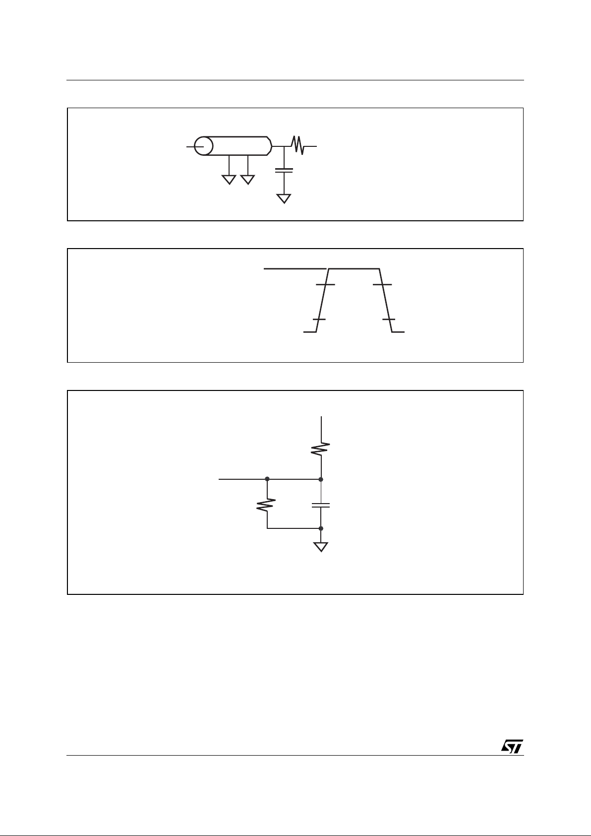
Figure 5. M7020R 2.5, or 3.3V AC Testing Load
Figure 6. M7020R 2.5, or 3.3V Input Waveform
Figure 7. M7020R 2.5, or 3.3V I/O Output Load Equivalent
Note: 1. Output loading is specified with CL = 5pF as in Fig ure 7. Transit i on i s measured at ± 200 mV from s teady-stat e voltage.
2. The load used for V
OH
, VOL testing is shown in Figur e 7.
C
L
VL = 1.25V for V
DDQ
= 2.5V
VL = 1.50V for V
DDQ
= 3.3V
50ΩZ0 = 50Ω
D
OUT
AC Load
AI05653
+2.5V V
DDQ
= 2.5V /
+3.0V V
DDQ
= 3.3V
90%
10%
90%
10%
GND
AI04299
208Ω for V
DDQ
= 2.5V
158Ω for V
DDQ
= 3.3V
192Ω for V
DDQ
= 2.5V
175Ω for V
DDQ
= 3.3V
AI04266
5pF
Q
V
DDQ
For Hi-Z and VOL/V
OH
(1, 2)
15/150
M7020R
Table 5. Capacitance
Note: 1. Effective capacitance measured with power suppl y. Sampled only, not 100% tested.
2. At 25°C, f = 1MHz.
3. Outputs deselect ed.
Table 6. DC Characteristics
Note: 1. Valid for A m bi ent Operat in g T emperat ure: TA = 0 to 70°C; VDD = 1.5V.
Symbol Parameter
Test Condition
(1,2)
Min Max Unit
C
IN
Input Capacitance
V
IN
= 0V
6pF
C
IO
(3)
Output Capacitance
V
OUT
= 0V
6pF
Sym Parameter
Test Condition
(1)
Min Max Unit
I
LI
Input Leakage Current
V
DDQ
= V
DDQ
(max), VIN = 0 to V
DDQ
(max)
±10 µA
I
LO
Output Leakage Current
V
DDQ
= V
DDQ
(max), VIN = 0 to V
DDQ
(max)
±10 µA
V
IL
Input Low Voltage (V
DDQ
= 3.3V)
–0.3 0.8 V
V
IH
Input High Voltage (V
DDQ
= 3.3V)
2.0
V
DDQ
+ 0.3
V
V
IL
Input Low Voltage (V
DDQ
= 2.5V)
–0.3 0.7 V
V
IH
Input High Voltage (V
DDQ
= 2.5V)
1.7
V
DDQ
+ 0.3
V
V
OL
Output Low Voltage (V
DDQ
= 3.3V) V
DDQ
= V
DDQ
(min), IOL = 8mA
0.4 V
V
OH
Output High Voltage (V
DDQ
= 3.3V) V
DDQ
= V
DDQ
(min), IOH = 8mA
2.4 V
V
OL
Output Low Voltage (V
DDQ
= 2.5V) V
DDQ
= V
DDQ
(min), IOL = 8mA
0.4 V
V
OH
Output High Voltage (V
DDQ
= 2.5V) V
DDQ
= V
DDQ
(min), IOH = 8mA
2.0 V
I
DD1
1.8V Supply Current at VDD(max)
66MHz Search Rate 2300 mA
50MHz Search Rate 1800 mA
I
DD2
3.3V Supply Current at VDD(max)
66MHz Search Rate, I
OUT
= 0mA
200 mA
50MHz Search Rate, I
OUT
= 0mA
150 mA
I
DD2
2.5V Supply Current at VDD(max)
66MHz Search Rate, I
OUT
= 0mA
160 mA
50MHz Search Rate, I
OUT
= 0mA
120 mA
M7020R
16/150
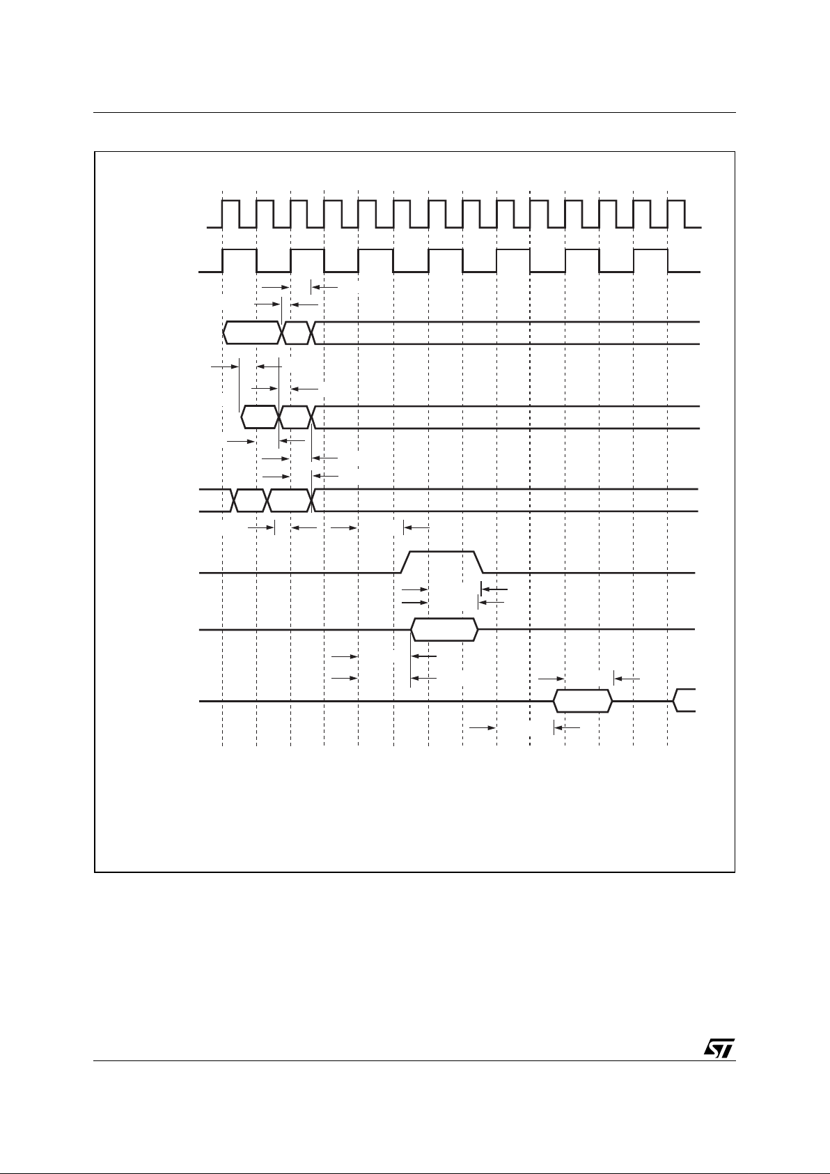
Figure 8. AC Timing Waveforms with CLK2X
Cycle
1
Cycle
0
Cycle
2
Cycle
3
Cycle
4
Cycle
5
Cycle
7
Cycle
6
Cycle
8
Cycle
10
Cycle
12
Cycle
9
Cycle
11
CLK2X
Signal
Group 0
Signal
Group 2
Signal
Group 3
Signal
Group 4
Signal
Group 5
CLK
AI04265
Signal Group 0: PHS_L, RST_L
Signal Group 1: DQ, CMD, CMDV
Signal Group 2: LHI, BHI, FULI
Signal Group 3: LHO, BHO, FULO, FULL
Signal Group 4: SADR, CE_L, OE_L, WE_L, ALE_L, SSF, SSV
Signal Group 5: DQ, ACK, EOT
tICSCH
tCKHOV
tCKHSV
tCKHSHZ
tCKHSLZ
tCKHOV
tIHCH
tISCH
tCKHDZ
tCKHDV
Signal
Group 1
tICHCH
tIHCH
tISCH
tISCH
tIHCH
tIHCH
17/150
M7020R
Table 7. AC Timing Parameters with CLK2X
Note: 1. Valid for A m bi ent Operat in g T emperat ure: TA = 0 to 70°C; VDD = 1.8V.
2. Values are based on 50% signal lev el s.
3. Base d on an AC load of C L = 30pF (see Figure 5, Figure 6, and Figur e 7, page 14).
4. These parameters are sampl ed and not 100% tested, and are based on an AC lo ad of 5pF.
Row Symbol
M7020R-050 M7020R-066 M7020R-083
Unit
Description
(1)
Min Max Min Max Min Max
1
f
CLOCK
100 133 166 MHz CLK2X frequency
2
t
CLK
10 7.5 ns CLK2X period
3
t
CKHI
4.0 3.0 ns
CLK2X high pulse
(2)
4
t
CKLO
4.0 3.0 ns
CLK2X low pulse
(2
5
t
ISCH
2.5 2.5 2.5 ns
Input Setup Time to CLK2X rising edge.
(2)
6
t
IHCH
0.6 0.6 0.6 ns
Input Hold Time to CLK2X rising edge.
(2)
7
t
ICSCH
4.2 4.2 4.2 ns
Cascaded Input Setup Time to CLK2X rising
edge.
(2)
8
t
ICHCH
0.6 0.6 0.6 ns
Cascaded Input Hold Time to CLK2X rising
edge.
(2)
9
t
CKHOV
9.5 8.5 ns
Rising edge of CLK2X to LHO, FULO, BHO,
FULL valid.
(3)
10
t
CKHDV
10.0 9.0 ns
Rising edge of CLK2X to DQ valid.
(2)
11
t
CKHDZ
1.2 9.5 1.2 9.5 1.2 9.5 ns
Rising edge of CLK2X to DQ high-Z.
(4)
12
t
CKHSV
10.0 9.0 ns
Rising edge of CLK2X to SRAM Bus valid.
(2)
13
t
CKHSHZ
7.0 6.5 ns
Rising edge of CLK2X to SRAM Bus highZ.
(2,4)
14
t
CKHSLZ
7.5 7.0 ns
Rising edge of CLK2X to SRAM Bus lowZ.
(2,4)

M7020R
18/150
OPERATION
The following subsections contain command
(CMD and DQ Bus (command and databus), database entry, arbitration logic, pipeline, and SRAM
control, and full logic descriptions.
CMD Bus and DQ Bus
CMD[8:0] carries the CMD and its associated parameter. DQ[67:0] is used for data t ransfer to and
from the database en tries, wh ich com prise a dat a
and a mask fiel d that are organized a s data and
mask arrays. The DQ Bus carries the SEARCH
data (of the data and mask arrays and internal registers) during the SEARCH command as well as
the address and data during READ and/or WRITE
operations. The DQ Bus can also carry the address information for the flow-through accesses to
the external SRAMs and/or SSRAMs.
Database Entry (Data Array and Mask Array)
Each database ent ry comprises a data and a mask
field. The resultant value of the entry is ’1,' ’0,’ or
’X (don’t care),’ depending on the value in the data
and mask bits. The on-chip priority encoder selects the first matching entry in the da tabase that
is nearest to location '0.'
Arbitrati on L ogi c
When multiple Search Engines are cascaded to
create large databases, the data being searched is
presented to all search engines simultaneously in
the cascaded system. If multiple matches occur
within the cascaded devices, arbitration log ic on
the search engin es w ill e nable the winning devic e
(with a matching entry that is closest to address “0”
of the cascaded database) to drive the SRAM bus.
Pipeline an d SR AM Control
Pipeline latency is added to give enough time to a
cascaded system’s arbitration logic to determ ine
the device that will drive the index of the matching
entry on the SRAM bus. Pipeline logic adds latency to both the SRAM access c ycles and the SSF
and SSV signals to align them to the host ASIC receiving the associated data.
Full Logic
Bit[0] in each of the 68-bit entries has a special
purpose for the LEARN command (0 = empty, 1 =
full). When all the data ent ries have bit[0] = 1, t he
database asserts the FULL Flag, indicating all the
search engines in the depth-cascade d array are
full.

19/150
M7020R
CONNECTION DESCRIPTIONS
Clocks and Reset
Master Clock (CLK2X). M7020R samples all the
data and control pins on the positive edge of
CLK2X. All signals are driven out of the device on
the rising edge of CLK2X (when PHS_L is low).
Phase (PHS_L). This signal runs at half the frequency of CLK2X and generates an internal CLK
from CLK2X see Figure 9, page 20.
Test Input (TEST - for Cypress Semiconductor
Use Only). This signal should be connected to
ground.
Reset (RST_L). Driving RS T_L low initial ize s the
device to a known state.
CMD and DQ Bus
CMD Bus (CMD[8:0]. [1:0] specifies the com-
mand; [8:2] contains the CMD parameters. The
descriptions of individual comm ands explains the
details of the parameters. The enc oding of commands based on the [1:0] field are:
– 00: PIO READ
– 01: PIO WRITE
– 10: SEARCH
–11: LEARN
CMD Valid (
CMDV). Qualifies the CMD bus:
– 0: No Command
– 1: Command
Address/Data Bus (
DQ[67:0]). This signal carries
the READ and WRITE address and data during
register, data, and mask array o perations. It carries the compare data during SEARCH operations. It also carries the SRAM address during
SRAM PIO accesses.
READ Acknowledge (ACK). This signal indicates that valid data is available on the DQ Bus
during register, data, and mask array READ operations, or the data is available on the SR AM data
bus during SRAM READ operations.
Note: ACK Signals require a weak external pulldown resistor such as 47 or 100 KΩ.
End of Transfe r (E OT) . This signal indicates the
end of burst transfer to the data or mask array during READ or WRITE burst operations.
Note: EOT Signals require a weak external pulldown resistor such as 47 KΩ or 100 KΩ.
SEARCH Successful Flag (SSF). When asserted, this signal indicates that the device is the global winner in a SEARCH operation.
SEARCH Successful Flag Valid (SSV). When
asserted, this signal qualifies the SSF signal.
SRAM Interface
SRAM Address (SADR[21:0]). This bus con-
tains address lines to access off-chip SRAMs that
contain associative data. See Tab le 50, page 127
for the details of the generated SRAM address. In
a database of multiple M7020Rs, each corresponding bit of SADR from all cascaded devices
must be connected.
SRAM Chip Enable (CE_L). This is chip ena ble
control for external SRAMs. In a database o f multiple M7020Rs, CE_L of all cascaded devices
must be connected. This signal is then driven by
only one of the devices.
SRAM Write Enable (WE_L). This is write enable control for external SRA M s. In a database of
multiple M7020Rs, WE_L of all cascaded devices
must be connected together. This signal is then
driven by only one of the devices.
SRAM Output Enable (OE_L). This is output enable control for external SRAMs. Only the last device drives this signal (with the LRAM bit set).
Address Latch Enable (ALE_L). When this signal is low, the addresses are valid on the SR AM
Address Bus. In a database of multiple M7020Rs,
the ALE_L of all cascaded devices mu st be connected. This signal is then driven by only one of
the devices.
Cascade Interface
Local Hit In (LHI[6:0]). These pins depth-cas-
cade the device to form a larger table siz e. One
signal of this bus is c onnected to the LHO[1] or
LHO[0] of each of the upstream devices in a block.
All unused LHI pins are conn ected to a logic '0.'
(For more information, see DEPTH-CASCADING,
page 122.)
Local Hit Out (LHO[1:0]). LHO[1] and LHO[0]
are the same logical signal. LHO[1] or LHO[0] is
connected to one input of the LHI bus of up to four
downstream devices in a bl ock of up to ei ght devices. (For more information, see DEPTH-CASCADING, page 122.)
Block Hit In (BHI[2:0]). Inputs from t he previous
BHO[2:0] are tied to the BHI[2:0] of the current device. In a four-block system, the last block can
contain only seven devices bec ause the ID code
11111 is used for broadcast access.
Block Hit Out (BHO[2:0]). These outputs from
the last device in a block are connected to the
BHI[2:0] inputs of the devices in the downstream
blocks.
Full In (FULI[6:0]). Each signal in this bus is connected to FULO[0] or FULO[1] of an upstream device to generate the FULL signal for the depthcascaded block.
M7020R
20/150
Full Out (FULO[1:0]). FULO[1] and FULO[0] are
the same logical signal. One of these two signals
must be connected to the FULI of up to four downstream devices in a depth-casc aded table. Bit [0]
in the data array indicates if the entry is full (1) or
empty (0).This signal is asserted if all of the bits in
the data array are ’1s.’ Refer to Depth-Cascading
to Generate a “FULL” Signal, page 122.
Full Flag (FULL). When asserted, t his signal in-
dicates that the table consisting of many depthcascaded devices is full .
Device Identification
Device Identification (ID[4:0]). The binary-en-
coded device ID for a depth-cascaded system
starts at 00000 and goes up to 11110. 11111 is reserved for a special broadcast address that selects all cascaded search engines in the system.
On a broadcast READ-only, the device with the
LDEV bit set to '1' responds.
Supplies
Chip Core Supply (V
DD
). This is equal to 1.8V.
Chip I/O Supply (V
DDQ
). This is equal to either
2.5 or 3.3V.
Test Access Port
Test Data In (TDI). This is the Test Access Port’s
Test Data In.
Test Clock (TCK). This is the Test Access Port’s
Test Clock.
Test Data Out (TDO). This is the Test Access
Port’s Test Data Out.
Test Mode Select (TMS). This is the Test Ac-
cess Port’ s T e st Mod e Select.
Test Reset (TRST_L). This is the Test Access
Port’s Test Reset.
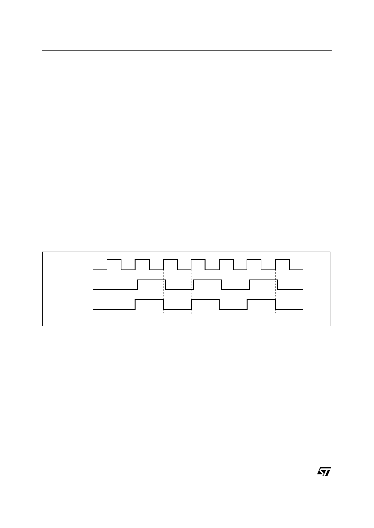
CLOCKS
The M7020R receives the CLK2X and PHS_L signals. It uses the PHS_L signal to divide CLK2X
and generate an internal clock (CLK), as shown in
Figure 9. The M7020R uses CLK2X and CLK for
internal operations.
Figure 9. Clocks (CLK2X and PHS_L)
Note: Any refe rence to “CLK Cycles” means 1 cycle of the signal, “CLK.”
1. “CLK” is an internal signal.
CLK2X
PHS_L
CLK
(1)
AI04750
21/150
M7020R
REGISTERS
All registers in the M 7020R are 6 8 bits wide. T he
M7020R contains 8 pairs of comparand storage
registers, 16 pairs of global mask registers
(GMRs), eight search successful index registers
and one each of CM D, information, burst READ,
burst WRITE, and next-free address registers. Table 8 provides an overview of all the M7020R registers. The registers are ordered in ascending
address order. Each register group is then described in the following subsections.
Table 8. Register Overview
Address Abbreviation Type Name
0–31 C OMP0–31 R
16 Comparand Registers. Stores comparands from the DQ Bus for
learning later.
32–47 MASKS RW 8 Global Mask Registers Array.
48–55 SSR0–7 R 8 SEARCH Successful Index Registers.
56 COMMAND RW Command Register.
57 INFO R Information Register.
58 RBURREG RW Burst Read Register.
59 WBURREG RW Burst Write Register.
60 NFA R Next Free Address Register.
61–63 – – Reserved
M7020R
22/150
Comparand Registers
The device contains 3 2 68-bit comparand registers (16 pairs) dynamically selected in every
SEARCH operation to store the comparand presented on the DQ Bus. The LEARN command will
later use these registers when executed. The
M7020R stores the SEARCH command’s Cycle A
comparand in the even-numbered register and the
Cycle B comparand in the odd-numbered register,
as shown in Figure 10.
Mask Registers
The device contains 16 68-bit global mask registers (8 pairs) dynamically selected in every
SEARCH operation to select the search subfield.
The addressing of these registers is explained in
Figure 11. The three-bit GMR Index supplied on
the CMD bus can apply 8 pairs of global masks
during the SEARCH and WRITE operations, as
shown in Figure 11.
Note: In 68-bit SEA RCH and WRITE opera tions,
the host ASIC must p rogram both the even and
odd mask registers with the same values.
Each mask bit in the GMRs is used during
SEARCH and WRITE operations. In SEARCH operations, setting the mask bit to '1' enables compares; setting the mask bit to '0' disables
compares (forced match) at the corresponding bit
position. In WRITE operations to the data or mask
array, setting the mask b it to '1' en ables WRITEs;
setting the mask bit to '0' disables W RITEs at the
corresponding bit position.
Figure 10. Comparand Register Selection
During SEARCH and LEARN
Instructions
Figure 11. Addressing the Global Masks
Register Array
135 0
6868
1
0
32
54
7
6
30 31
0
15
1
Address
Index
AI04275
135 0
6868
1
0
32
54
7
6
9
8
11
10
13
12
15
14
0
1
6
7
2
5
4
3
Address
Index
AI04276
SEARCH and WRITE Command
Global Mask Selection
23/150
M7020R
SEARCH-Successful Registers (SSR[0:7])
The device contains eight sea rch successful registers (SSRs) to hold the index of the location
where a successful search occurred. The format of
each register is described in Table 9. The
SEARCH command specifies which SSR stores
the index of a specific SE ARCH comma nd in Cycle B of the SEARCH Instruction. Subsequently,
the host ASIC can u se this register to acc ess that
data array, mask array, or external SRAM using
the index as part of the indirect access address
(see Table 19, page 32 and Table 22, page 35)
.
The device with a valid bit set performs a READ or
WRITE operation. All other devices suppress the
operation.
Table 9. SEARCH-Successful Register (SSR) Description
Field Range Initial Value Description
INDEX [14:0] X
Index. This is the address of the 68-bit entry where a successful
search occurs. The device updates this field only when a search is
successful. If a hit occurs in a 136-bit entry-size quadrant, the LSB is
’0.’ If a hit occurs in a 272-bit entry size quadrant, the two LSBs are
’00.’ This index updates if the device is either a local or global winner
in a SEARCH operation.
– [30:15] 0 Reserved.
VALID [31] 0
Valid. During SEARCH operation in a depth-cascaded configuration,
the device that is a global winner in a match sets this bit to '1.' This bit
updates only when the device is a global winner in a SEARCH
operation.
– [67:32] 0 Reserved.
M7020R
24/150
The Command Register
Table 10. Command Register Field Descriptions
Field Range Initial Value Description
SRST [0] 0
Software Reset. If ’1,’ this bit resets the device, with the same effect
as the hardware reset. Internally, it generates a reset pulse lasting for
eight CLK cycles. This bit automatically resets to a ’0’ the reset cycle
has completed.
DEVE [1] 0
Device Enable. If ’0,’ it keeps the SRAM Bus (SADR, WE_L, CE_L,
OE_L, and ALE_L), SSF, and SSV signals in 3-state condition and
forces the cascade interface output signals LHO[1:0] and BHO[2:0] to
’0.’ It also keeps the DQ Bus in input mode. The purpose of this bit is
to make sure that there are no bus contentions when the devices
power up in the system.
TLSZ [3:2] 01
Table Size. The host ASIC must program this field to configure the
chips into a table of a certain size. This field affects the pipeline
latency of the SEARCH and LEARN operations as well as the READ
and WRITE accesses to the SRAM (SADR[21:0], CE_L, OE_L,
WE_L, ALE_L, SSV, SSF, and ACK). Once programmed, the search
latency stays constant.
TLSZ [3:2] 01
Latency in #
of CLK Cycles
00: 1 device 4
01: 2-8 devices 5
10: 9-31 devices 6
11: Reserved
HLAT [6:4] 000
Latency of Hit Signals. This field adds latency to the SSF and SSV
signals during SEARCH, and ACK signal during SRAM READ access
by the following number of CLK cycles.
000: 0 100: 4
001: 1 101: 5
010: 2 110: 6
011: 3 111: 7
LDEV [7] 0
Last Device in the Cascade. When set, this device is the last device
on the SRAM bus in the depth-cascaded table and is the default driver
for the SSF and SSV signals.
In the event of a SEARCH failure, the device with this bit set drives the
hit signals as follows:
SSF = 0, SSV = 1
During non-SEARCH cycles, the device with this bit set drives the
signals as follows:
SSF = 0, SSV = 0
LRAM [8] 0
Last device on this SRAM Bus. When set, this device is the last
device on this SRAM bus in the depth-cascaded table and is the
default driver for the SADR, CE_L, WE_L, and ALE_L signals. In
cycles where no M7020R device in a depth-cascaded table drives
these signals, this device drives the signals as follows:
SADR = 3FFFFF,
CE_L = 1
WE_L = 1
ALE_L = 1
OE_L is always driven by the device for which this bit is set.
25/150
M7020R
The Information Register
Table 11. Information Register Field Descriptions
Note: 1. This field may change in future ve rsions.
CFG [16 :9]
0000
0000
Database Configuration. The device is internally divided into four
quadrants of 8K x 68, each of which can be configured as 8K x 68, 4K
x 136, or 2K x 272 as follows:
00: 8K x 68
01: 4K x 136
10: 2K x 272
11: Reserved
Bits [10:9] apply to configuring the 1st quadrant in the address space.
Bits [12:11] apply to configuring the 2nd quadrant in the address
space.
Bits [14:13] apply to configuring the 3rd quadrant in the address
space.
Bits [16:15] apply to configuring the 4th quadrant in the address
space.
[67:17] 0 Reserved.
Field Range Initial Value Description
Field Range Initial Value Description
Revision [3:0]
0001
(1)
Revision Number. This is the current device revision
number. Numbers start from one and increment by one
for each revision of the device.
Implementation [6:4] 001 This is the M7020R implementation number.
Reserved [7] 0 Reserved.
Device ID [11:8] 0001 or 0010 This is the Device Identification Number.
Device ID [12] Reserved
Device ID [15:13] 00000100 This is the Device Identification Number.
MFID [31:16] 1101_1100_0111_1111
Manufacturer ID. This field is the same as the
manufacturer ID and continuation bits in the TAP
controller.
[67:32] Reserved.
M7020R
26/150
The Read Burst Address Register (RBURREG)
These READ burst address register fields must be
programmed before burst READ (see Table 12).
The Write Burst Address Register (WBURREG)
These WRITE burst a ddress register fields must
be programmed before burst W RITE (see Table
13).
The NFA Register
Bit [0] of each 68-bit data entry is a special bit designated for use in the operation of the LEARN
command. In 68-bit quadrant s, the bi t[0] indi cates
whether a location is full (bit set to ’1’ ) or empty (bit
set to ’0’). Every WRITE/LEARN command loads
the address of first 68-bit location that cont ains a
'0' in the entry’s bit[0]. This i s stored in the NFA
register (see Table 14). If all the bits in a device are
set to '1,' the M7020R asserts FULO[1:0] to '1.'
In 136-bit-configured quadrants, the LSB of this
register is always set to '0.' The host ASIC must
set bit '0' and Bit 68in a 136-bit word to either '0' or
'1' to indicate full/empty status.
Note: Both bits (0 and 68) must be set to '0' or '1'
(e.g., '10' or '01' settings are invalid).
Table 12. Read Burst Register Description
Table 13. Write Burst Register Description
Table 14. NFA Register
Field Range Initial Value Description
ADR [14:0] 0
Address. This is the starting address of the data array or mask array
during a burst READ operation. It automatically increments by 1 for
each successive read of the data array or mask array. Once the
operation is complete, the contents of this field must be reinitialized for
the next operation.
[18:15] Reserved.
BLEN [27:19] 0
Length of Burst Access. The device is capable of writing from 4 up
to 511 locations in a single burst. The BLEN decrements
automatically. Once the operation is complete, the contents of this
field must be reinitialized for the next operation.
[67:28] Reserved.
Field Range Initial Value Description
ADR [14:0] 0
Address. This is the starting address of the data array or mask array
during a burst WRITE operation. It automatically increments by 1 for
each successive write of the data array or mask array. Once the
operation is complete, the contents of this field must be reinitialized for
the next operation.
[18:15] Reserved.
BLEN [27:19] 0
Length of Burst Access. The device is capable of writing from 4 up
to 511 locations in a single burst. The BLEN decrements
automatically. Once the operation is complete, the contents of this field
must be reinitialized for the next operation.
[67:28] Reserved.
Address 67 - 15 14 - 0
60 Reserved Index
27/150
M7020R
SEARCH ENGINE ARCHITECTURE
The M7020R consists of 32K x 68-bit storage cells
referred to as data bi t s. T here i s a mask cell corresponding to each data cell. Figure 12 shows the
three organizations of the device based on the value of the CFG bits in the command register.
During a SEARCH operation, the search data bit
(S), data array bit (D), mask array bit (M) and the
global mask bit (G) are used in the following manner to generate a mat ch at that bit position (see
Table 15, page 28).
The entry with all matched bit positions results in a
successful search during a SEARCH operation.
In order for a successful search within a device to
make the device the local winner in the SEARCH
operation, all 68-bit positions must generate a
match for a 68-bit entry in 68-bit-configured quadrants, or all 136-bit positions must generate a
match for two consecutive even and odd 68-bit entries in quadrants configured as 136 bits, or all
272-bit positions must generate a match for 4 consecutive entries aligned to 4 entry-page boundaries of 68-bit entries in quadrants configured as
272 bits.
An arbitration mechanism using a cascade bus determines the global winning device among the local winning devices in a SEARCH cycle. The
global winning device drives the SRAM Bus, SSV,
and the SSF signals. In case of a SEARCH failure,
the devices with the LDEV and LRAM bits set
drive(s) the SRAM Bus, SSF, and SSV signals.
The M7020R device can be configured to contain
tables of different widths, even within the same
chip. Figure 13, page 28 shows a sample configuration of different widths.
Data and Mask Addressing
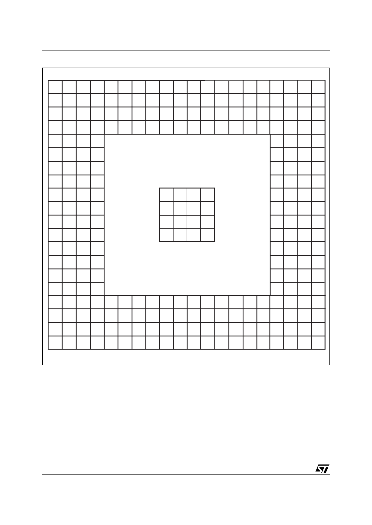
Figure 14, page 28 shows the M7020R data array
and mask array addressing procedure.
Figure 12. M7020R Database Width Configuration
Data
Data
Data
Masks
Masks
Masks
32 K
CFG = 00000000
CFG = 01010101
CFG = 10101010
68
136
272
16 K
8 K
AI04279
M7020R
28/150
Table 15. Bit Position Match Figure 13. Multi-width Configuration Example
Figure 14. M7020R Data and Mask Array Addressing
G M D S Match
0XXX1
10XX1
11001
11100
11010
11111
8 K
8 K
4 K
2 K
68
68
136
272
CFG = 10010000
AI04280
CFG = 00000000
CF G = 1010 1010
67 0
0
1
2
3
32767
271 0
3210
7654
32764 32765 32766 32767
68
CFG = 010 1010 1
135 0
10
32
54
76
32766 32767
(68-bit Configuration)
( 27 2- bi t c onf ig ur atio n)
(136-bit Configuration)
32 K
8K
16K
68 6868 68 6868
AI04281
29/150
M7020R
COMMAND CODES AND PARAMETERS
A master device, such as an ASIC controller, issues commands t o the M7020R using the Command Valid CMDV signal and the CMD Bus. The
following subsections describe the functions of the
commands.
Command Codes
The M7020R implements four basic commands
shown in Table 16. The Command Code must be
presented to CMD[1:0] while keeping the command valid (CMDV) signal high for two CLK2X cy-
cles. These two CLK2X cycles are designated as
“Cycle A” and “Cycle B.” The controller ASIC must
align the instructions wi th the PHS_L signal. The
CMD[8:2] field passes the parameters of the command in Cycles A and B.
Commands and Command Parameters
Table 17, page 29 li sts the CMD bus fields that
contain the M7020R command parameters as well
as their respective cycles.
Table 16. Command Codes
Table 17. Command Parame ters
Note: 1. The 272-bit -configured devices or 272-bit-configured quadrants within devices do not support the LEAR N Instruction.
CMD Code Command Description
00 READ
Reads one of the following: data array, mask array, device registers, or external
SRAM.
01 WRITE
Writes one of the following: data array, mask array, device registers, or external
SRAM.
10 SEARCH
Searches the data array for a desired pattern using the specified register from the
global mask register array and local mask associated with each data cell.
11 LEARN
The device has internal storage for up to 16 comparands that it can learn. The
device controller can insert these entries at the next free address (as specified by
the NFA register) using the LEARN Instruction.
Cmd Cyc 8 7 6 5 4 3 2 1 0
READ
A SADR[21] SADR[20] X 0 0 0
0 = Single
1 = Burst
00
B0 0 0 000
0 = Single
1 = Burst
00
WRITE
A SADR[21] SADR[20] X
Global Mask
Register Index [2:0]
0 = Single
1 = Burst
01
B0 0 0
Global Mask
Register Index [2:0]
0 = Single
1 = Burst
01
SEARCH
A SADR[21] SADR[20] SADR[19]
Global Mask
Register Index [2:0]
68-bit or 136-bit: 0
272-bit:
1 in 1st Cycle
0 in 2nd Cycle
10
B Successful Search Register Index[2:0] Comparand Register Index 1 0
LEARN
(1)
A SADR[21] SADR[20] X Comparand Register Index 1 1
B0 0
Mode
0: 68-bit
1: 136-bit
Comparand Register Index 1 1

M7020R
30/150
READ COMMAND
The READ can be a single read of a data arra y, a
mask array, an SRAM, or a register location
(CMD[2] = 0). It can be a burst READ (CMD[2] = 1)
or mask array locations using an internal auto-incrementing address register (RBURADR). Table
18, page 32 describes each t ype of READ command.
A single-location READ operation lasts six cycles,
as shown in Figure 15, page 31. T he bu rst RE A D
adds two cycles for each successive READ. The
SADR[21:20] bits supplied in the READ Instruction
Cycle A drive SADR[21:20] signals during the
READ of an SRAM location.
The single READ operation takes six CLK cycles,
in the following sequence:
– Cycle 1: The ho st ASIC applies the READ In-
struction on the CMD[1:0] (CMD[2] = 0), using
CMDV = 1, and the DQ Bus supplies the address, as shown in Table 19, page 32 and Table
20, page 33. The host ASIC selects the M7020R
for which ID[4:0] matches the DQ[25:21] lines. If
the DQ[25:21] = 1 1111, the host ASIC selects
the M7020R with the LDEV Bit set. The host
ASIC also supplies SADR[21:20] on CMD[ 8:7]
in Cycle A of the RE A D I nstruction if t he REA D
is directed to the external SRAM.
– Cycle 2: The ho st ASIC floats DQ[67:0] to 3-
state condition.
– Cycle 3: The host ASIC keeps DQ[67:0] in 3-
state condition.
– Cycle 4: The selected device starts to driv e the
DQ[67:0] Bus and drives the ACK signal from Z
to low.
– Cycle 5: The selected d evice drives the read
data from the addressed location on the
DQ[67:0] Bus and drives the ACK signal high.
– Cycle 6: The selected device floats DQ[67:0] to
3-state condition and drives the ACK signal low.
At the termination of Cycle 6, the selected dev ice
releases the ACK line to 3-state condition. The
READ Instruction is complete, and a new operation can begin.
Note: The laten cy of the SR AM RE AD will be d ifferent than the one described ab ove (see SRAM
PIO Access, page 126). Table 19, page 32 lists
and describes the format of the READ address for
a data array, mask array, or SRAM.
In a burst READ operation, the READ lasts 4 + 2n
CLK-cycles (where “n” stands for the number of
accesses in the burst specified by the BLEN field
of the RBURREG). Table 20, page 33 describes
the READ address format for the internal registers.
Figure 16, page 31 illustrates the timing diagram
for the burst READ of the data or mask array. This
operation assumes that the host ASIC has programmed the RBURREG with the starting address
(ADR) and the length of transfer (BLEN) before initiating the burst READ command.
– Cycle 1: The ho st ASIC applies the READ In-
struction on the CMD[1:0] (CMD[2] = 1), using
CMDV=1 and the address supplied on the DQ
Bus, as shown in Ta ble 21, page 33. The h ost
ASIC selects the M7020R for which ID[4:0]
matches the DQ[25:21] lines. If the DQ[25:21] =
11111, the host ASIC selects the M70 20R with
the LDEV Bit set.
– Cycle 2: The host ASIC floats DQ[67:0] to the 3-
state condition.
– Cycle 3: The host ASIC keeps DQ[67:0] in t he
3-state condition.
– Cycle 4: The selected device starts to driv e the
DQ[67:0] Bus and drives ACK and E OT from Z
to low.
– Cycle 5: The selected dev ice drives the REA D
data from the addressed location on the
DQ[67:0] Bus and drives the ACK signal high.
Note: Cycles four and five repeat for each additional access until all the accesses specified in
the burst length (BLEN) field of RBURREG are
complete. On the last transfer, the M7020R
drives the EOT signal high.
– Cycle (4 + 2n): The selected device drives t he
DQ[67:0] to 3-state condition and drives the
ACK and the EOT signals low.
At the termination of Cycle 4 + 2n, the selected device floats the ACK line to 3 -state condition. The
burst READ Instruction is complete, and a new operation can begin (see Table 21, page 33 for burst
READ address formats).

31/150
M7020R
Figure 15. Single Location READ Cycle Timing
Figure 16. Burst READ of the Data and Mask Arrays (BLEN = 4)
Cycle 1 Cycle 2 Cycle 3 Cycle 4 Cycle 5 Cycle 6
CLK2X
CMDV
CMD[1:0]
ACK
DQ
PHS_L
AI04672
Read
CMD[8:2]
BA
Address
FF
Data
Cycle 1
Cycle 2
Cycle 3
Cycle 4
Cycle 5 Cycle 7
Cycle 6 Cycle 8 Cycle 10
Cycle 11
Cycle 12
Cycle 9
CLK2X
CMDV
CMD[1:0]
CMD[8:2]
ACK
EOT
DQ
PHS_L
AI04283
Read
BA
Address
FF
Data0
FF
Data1
FF
Data2
FF
Data3

M7020R
32/150
Table 18. READ Command Parameters
Table 19. Data and Mask Array, SRAM Read Address Forma t
Note: 1. “|” stands for Logic al OR operation. “{ }” stands for concatenation operator.
CMD Parameter
CMD[2]
Read Command Description
0 Single Read
Reads a single location of the data array, mask array, external SRAM,
or device registers. All access information is applied on the DQ Bus.
1 Burst Read
Reads a block of locations from the data array or mask array as a
burst.
The internal register (RBURADR) specifies the starting address and
the length of the data transfer from the data array or mask array , and it
auto-increments the address for each access.
All other access information is applied on the DQ Bus.
Note: The device registers and external SRAM can only be read in
single-read mode.
DQ
[67:30]
DQ
[29]
DQ
[28:26]
DQ
[25:21]DQ[20:19]DQ[18:15]
DQ
[14:0]
Reserved
0: Direct
1: Indirect
Successful SEARCH
Register Index
(Applicable if DQ[29]
is indirect)
ID
00: Data
Array
Reserved
If DQ[29] is ’0,’ this field carries
address of data array location.
If DQ[29] is ’1,’ the successful
search register ID (SSRI)
specified on DQ[28:26] supplies
the address of the data array
location:
{SSR[14:2], SSR[1] | DQ[1],
SSR[0] | DQ[0]}
(1)
Reserved
0: Direct
1: Indirect
Successful SEARCH
Register Index
(Applicable if DQ[29]
is indirect)
ID
01: Mask
Array
Reserved
If DQ[29] is ’0,’ this field carries
address of mask array location.
If DQ[29] is ’1,’ the successful
search register ID (SSRI)
specified on DQ[28:26] supplies
the address of the mask array
location:
{SSR[14:2], SSR[1] | DQ[1],
SSR[0] | DQ[0]}
(1)
Reserved
0: Direct
1: Indirect
Successful SEARCH
Register Index
(Applicable if DQ[29]
is indirect)
ID
10:
External
SRAM
Reserved
If DQ[29] is ’0,’ this field carries
address of SRAM location.
If DQ[29] is ’1,’ the successful
search register ID (SSRI)
specified on DQ[28:26] supplies
the address of the SRAM
location:
{SSR[14:2], SSR[1] | DQ[1],
SSR[0] | DQ[0]}
(1)

33/150
M7020R
Table 20. READ Address Format for Internal Registers
Table 21. READ Address Format for Data and Mask Arrays
WRITE COMMAND
The WRITE can be a single write of a d ata array,
mask array, register, or external SRAM location
(CMD[2] = 0). It can be a burst WRITE
(CMD[2] = 1) using an internal auto-incrementing
address register (WBURADR) of the data array or
mask array locations. A single-location WRITE is a
three-cycle operation, shown in Figure 17, page
34. The burst WRITE adds one extra cycle for
each successive WRITE.
The WRITE operation sequence is as follows:
– Cycle 1A: The host ASIC applies the WRITE In-
struction on the CMD[1:0] (CMD[2] = 0), using
CMDV=1 and the address supplied on the DQ
Bus, as shown in Ta ble 22, page 35. The ho st
ASIC also supplies the index to the global mask
register to mask the write to the data array or
mask array location in CMD[5:3]. For SRAM
WRITEs, the host ASIC must supply the
SADR[21:20] on CMD[8:6]. The host ASIC sets
CMD[9] to '0' for the normal WRITE.
– Cycle 1B: The host ASIC continues to apply the
WRITE Instruction to the CMD[1:0]
(CMD[2] = 0), using CMDV = 1 and the address
supplied on the DQ Bus. The host ASIC continues to supply the global m ask register i ndex to
mask the WRITE to the data or mask arr ay locations in CMD[5:3]. The host ASIC selects the
device where ID[4:0] matches the DQ[25:21]
lines, or it selects all the devices when
DQ[25:21] = 11111.
– Cycle 2: The host ASIC drives the DQ[67:0]
with the data to be written to the data array,
mask array, external SRAM, or register location
of the selected device.
– Cycle 3: Idle cycle. At the termination of this cy-
cle, another operation can begin.
Note: The latency of the SRAM WRITE will be
different than the one described above (see
SRAM PIO Access, page 126).
The burst WRITE operation lasts for n + 2 CLK cycles (where n signifies the number of accesses in
the burst as specified in the BLEN field of the
WBURREG register, please see Figure 18, page
35).
This operation assumes that the host ASIC has
programmed the WBURREG with the starting address (ADR) and the length of transfer (BLEN) before initiating the burst write command (see Ta ble
24, page 36 for format). The sequence is as follows:
– Cycle 1A: The host ASIC applies the WRITE In-
struction on the CMD[1:0] (CMD[2] = 1), using
CMDV = 1 and the address supplied on the DQ
Bus, as shown in Ta ble 24, page 36. The h ost
ASIC also supplies the index to the global mask
register to mask the write to the data or mask array locations in CMD[5:3].
– Cycle 1B: The host ASIC continues to apply the
WRITE Instruction on the CMD[1:0]
(CMD[2] = 0), using CMDV = 1 and the address
supplied on the DQ Bus. The host ASIC continues to supply the global m ask register i ndex to
mask the WRITE to the data or mask arr ay locations in CMD[5:3]. The host ASIC selects the
device where ID[4:0] matches the DQ[25:21]
lines, or it selects all the devices when
DQ[25:21] = 11111.
DQ[67:26] DQ[25:21] DQ[20:19] DQ[18:6] DQ[5:0]
Reserved ID 11: Register Reserved Register Address
DQ[67:26] DQ[25:21] DQ[20:19] DQ[18:15] DQ[14:0]
Reserved ID 00: Data Array Reserved
Do not care. These 15 bits come from the internal
register (RBURADR) which increments for each
access.
Reserved ID
01: Mask
Array
Reserved
Do not care. These 16 bits come from the internal
register (RBURADR) which increments for each
access.

M7020R
34/150
– Cycle 2: The host ASIC drives the DQ[67:0]
with the data to be written to the data array or
mask array location of the selected device. The
M7020R writes the data f rom the DQ[67:0] Bus
only to the subfield that has the corresponding
mask bit set to '1' in the global mask register
specified by the index CMD[5:3] and supplied in
Cycle 1.
– Cycles 3 to n + 1: The host ASIC drives the
DQ[67:0] with the data to be written to the next
data array or mask array location (addressed by
the auto-increment ADR field of the WBURREG
register) of the selected device.
The M7020R wri tes the data on the DQ[67:0]
Bus only to the subfield that has the corresponding mask bit set to '1' in the global mask register
specified by the index CMD[5:3] and supplied in
Cycle 1. The M7020R drives the EOT signal low
from Cycle 3 to Cycle n; the M7020R drives the
EOT signal high in Cycle n + 1 (n is specified in
the BLEN field of the WBURREG).
– Cycle n + 2: The M7020R drives the EOT signal
low. At the termination of the Cycle n + 2, the
M7020R floats the EOT sign al to a 3-state, and
a new instruction can begin.
Figure 17. Sin gl e Location WRI TE Cy c le Timing
Cycle 1 Cycle 2 Cycle 3 Cycle 4Cycle 0
CLK2X
CMDV
CMD[1:0]
DQ
PHS_L
AI04284
Write
CMD[8:2]
BA
Address
Data
X

35/150
M7020R
Figure 18. Burst WRITE of the Data and Mask Arrays (BLEN = 4)
Table 22. (Single) WRITE Address Format for Data and Mask Arrays or SRAM
Note: 1. “|” stands for Logic al OR operation. “{ }” stands for concatenation operator.
DQ
[67:30]
DQ
[29]
DQ
[28:26]
DQ
[25:21]
DQ
[20:19]
DQ
[18:15]
DQ
[14:0]
Reserved
0: Direct
1: Indirect
Successful
SEARCH
Register
Index
(Applicable
if DQ[29] is
indirect)
ID
00: Data
Array
Reserved
If DQ[29] is ’0,’ this field carries the
address of the data array location.
If DQ[29] is ’1,’ the successful
search register specified by
DQ[28:26] supplies the address of
the data array location:
{SSR[14:2], SSR[1] | DQ[1], SSR[0]
| DQ[0]}
(1)
Reserved
0: Direct
1: Indirect
Successful
SEARCH
Register
Index
(Applicable
if DQ[29] is
indirect)
ID
01: Mask
Array
Reserved
If DQ[29] is ’0,’ this field carries
address of the mask array location.
If DQ[29] is ’1,’ the successful
search register specified by
DQ[28:26] supplies the address of
the mask array location:
{SSR[14:2], SSR[1] | DQ[1], SSR[0]
| DQ[0]}
(1)
Reserved
0: Direct
1: Indirect
Successful
SEARCH
Register
Index
(Applicable
if DQ[29] is
indirect)
ID
10:
External
SRAM
Reserved
If DQ[29] is ’0,’ this field carries
address of the data SRAM location.
If DQ[29] is ’1,’ the successful
search register specified by
DQ[28:26] supplies the address of
the SRAM location:
{SSR[14:2], SSR[1] | DQ[1], SSR[0]
| DQ[0]}
(1)
Cycle 1 Cycle 2 Cycle 3 Cycle 4 Cycle 5 Cycle 6
CLK2X
CMDV
CMD[1:0]
EOT
DQ
PHS_L
AI04285
Write
CMD[8:2]
BA
Address
Data0
Data1
Data2
Data3
X

M7020R
36/150
Table 23. WRITE Address Format for Internal Registers
Table 24. WRITE Address Format for Data and Mask Array (Burst Write)
SEARCH COMMAND
The M7020R (Silicon) Search Engine can be configured in ten ways:
– 68-bit SEARCH on tables configured as x68
using one device
– 68-bit SEARCH on tables configured as x68
using up to 8 devices
– 68-bit SEARCH on tables configured as x68
using up to 31 devices
– 136-bit SEARCH on tables configured as
x136 using one device
– 136-bit SEARCH on tables configured as
x136 using up to 8 devices
– 136-bit SEARCH on tables configured as
x136 using up to 31 devices
– 272-bit SEARCH on tables configured as
x272 using one devices
– 272-bit SEARCH on tables configured as
x272 using up to 8 devices
– 272-bit SEARCH on tables configured as
x272 using up to 31 devices
– Mixed-sizes on tables configured with differ-
ent widths using an M7020R
68-bit Configuration with Single Device
The hardware diagram of the search subsystem of
a single device is shown in Figure 19. Fi gure 20,
page 38 shows the timing diagram for a SEARCH
operation in the 68-bit configuration (CFG =
00000000) for one set of parameters. This illustra-
tion assumes that the host ASIC has programmed
TLSZ to '00,' HLAT to '000,' LRAM to '1,' and LDEV
to '1' in the command register.
The following is the sequence of operat ions for a
single 68-bit SEARCH command.
– Cycle A: The host ASIC drives CMDV high and
applies the SEARCH comm and code ('10') on
CMD[1:0] signals. CMD[5:3] must be driven with
the index to the global mask register pair for use
in the SEARCH operation. CMD[8:7] signals
must be driven with the same bits that will be
driven on SADR[21:20] by this device if it has a
hit. DQ[67:0] must be driven with t he 68-bi t data
to be compared. The CMD[2] signal must be
driven to Logic '0.'
– Cycle B: The host ASIC continues to drive
CMDV high and applies the SEARCH command
('10') on CMD[1:0]. CMD[5:2] must be driven by
the index of the comparand register pair for storing the 136-bit word presented on the DQ Bus
during Cycles A and B. CMD[8:6] signals must
be driven with the index of the SSR that will be
used for storing the address of the matching entry and the Hit Flag (see SEARCH-Successful
Registers (SSR[0:7]), page 23). The DQ [67:0]
continues to carry the 68-bit data to be compared.
Note: In the 68-bit configuration, the host A SIC
must supply the same da ta on DQ[67:0] du ring
both Cycles A and B. The even and odd pair of
GMRs selected for the comparison must be programmed with the same value.
DQ[67:26] D Q[25:21] DQ[20:19] DQ[18:6] DQ[5:0]
Reserved ID 11: Register Reserved Register address
DQ
[67:26]
DQ
[25:21]
DQ
[20:19]
DQ
[18:15]
DQ
[14:0]
Reserved ID 00: Data array Reserved
Don’t care. These 15 bits come from the internal
register (WBURADR), which increments with each
access.
Reserved ID
01: Mask
array
Reserved
Don’t care. These 15 bits come from the internal
register (WBURADR), which increments with each
access.

37/150
M7020R
The logical 68-bit SEARCH operation is shown in
Figure 21, page 39. The entire table consisting of
68-bit entries is compared to a 68-bit word K (presented on the DQ Bus in both Cycle s A and B of
the command) using the GMR and the local mask
bits. The effective GMR is the 68-b it word specified by the identical value in both even and odd
GMR pairs selected by the GMR Index in the com-
mand’s Cycle A. The 68 -bit word K (presen ted on
the DQ Bus in both Cycles A and B of the command) is also stored in both even and odd comparand register pairs selected by the Comparand
Register Index in the command’s Cycle B. In a x68
configuration, only the even comparand register
can be subsequently used by the LEARN command. The word K (presented on the DQ Bus in
both Cycles A and B of the command) is compared
with each entry in the table starting at location “0.”
The first matching entry’s location address, “L,” is
the winning address that is driven as part of the
SRAM address on the SADR[21:0] lines (see
SRAM ADDRESSING, page 126).
The SEARCH com mand is a pipelined o peration
and executes a SEARCH at half the rate of the frequency of CLK2X for 68-bit searches in x68-configured tables. The latency of SADR, CE_L,
ALE_L, WE_L, SSV, and SSF from the 68-bit
SEARCH command cycle (two CLK2X cycles) is
shown in Table 25, page 39.
The latency of a SEARCH from command to
SRAM access cycle is 4 for a single device in the
table and TLSZ = 00 . In addition, SSV and SSF
shift further to the right for different values of
HLAT, as specified in Table 26, page 39.
Figure 19. Hardware Diagram for a Table with One Device
DQ[67:0]
CMDV, CMD[8:0]
SSF, SSV
SRAM
BHI[2:0]
BHI[2:0]
LHO[1]
LHI
3210
M7020R
LHO[0]
654
AI05664

M7020R
38/150
Figure 20. Timing Diagram for a 68-bit Configuration SEARCH for One Device
Cycle 1
Cycle 2
Cycle 3
Cycle 4
Cycle 5 Cycle 7
Cycle 6 Cycle 8 Cycle 10
Cycle 9
CLK2X
CMDV
CMD[1:0]
CE_L
WE_L
OE_L
SADR[23:0]
SSV
SSF
CMD[8:2]
PHS_L
ALE_L
AI04286
A
B
A
B
A
B
A
B
DQ
D1 D2
D3
A1
A3
D4
Search3
Hit
Search4
Miss
Search1
Hit
Search2
Miss
CFG = 00000000, HLAT = 000, TLSZ = 00, LRAM = 1, LDEV = 1
Search1
Search2
Search3
Search4
01
01
01
01
1
1
1
1
1
0
0
0
1
1
1
0
0
0
0
0
1
1
0
0
0
0
1
1
1
1
0
0

39/150
M7020R
Figure 21. x68 Table with One Device
Table 25. Latency of SEARCH from Instruction to SRAM Access Cycle, 68-bit, 1 Device
Table 26. Shift of SSF and SSV from SADR
# of devices Max Table Size Latency in CLK Cycles
1 (TLSZ = 00) 32K x 68-bit 4
2–8 (TLSZ = 01) 256K x 68-bit 5
9–31 (TLSZ = 10) 992K x 68-bit 6
HLAT Number of CLK Cycles
000 0
001 1
010 2
011 3
100 4
101 5
110 6
111 7
Comparand Register (even)
Comparand Register (odd)
67
0
K
CFG = 00000000
0
1
2
3
32767
(68- bi t Configuration)
Location
address
L
K
Comparand Register (even)
67
0
K
GMR
67
0
AI05665
(First matching entry)

M7020R
40/150
68-bit SEARCH on Tables Configured as x68 Using up to Eight M7020R Devices
The hardware diagram of the search subsystem of
eight devices is shown in Figure 22, page 41. The
following are the parameters programmed into the
eight devices:
– First seven devices (device 0–6):
CFG = 00000000, TLSZ = 01, HLAT = 010,
LRAM = 0, and LDEV = 0.
– Eighth device (device 7):
CFG = 00000000, TLSZ = 01, HLAT = 010,
LRAM = 1, and LDEV = 1.
Note: All eight devices m ust b e program m ed with
the same values for TLSZ and HLAT. Only the last
device in the table (Device 7 in this case) must be
programmed with LRAM = 1 and LDEV = 1. All
other upstream devices (Devices 0 through 6 in
this case) must be programmed with LRAM = 0
and LDEV = 0.
Figure 24, page 43 shows the timing diagram for a
SEARCH command in the 68-bi t-configured table
of eight devices for Device 0. Figure 25, page 44
shows the timing diagram for a SEARCH command in the 68-bit-configured table of eight devices for Device 1. Figure 26, page 45 shows the
timing diagram for a SEARCH command in the
68-bit-configured table of eight devices for Device
7 (the last device in this specific tabl e). For these
timing diagrams four 68-bit searches are performed sequentially. HIT/MISS assumptions were
made as shown below in Table 27.
The sequence of operation for a 68 -bit SEARCH
command is as follows:]
– Cycle A: The host ASIC drives CMDV high and
applies the SEARCH comm and code ('10') on
CMD[1:0] signals. CMD[5:3] must be driven with
the index to the global mask register pair for use
in the SEARCH operation. CMD[8:7] signals
must be driven with the same bits that will be
driven on SADR[23:21] by this device if it has a
hit. DQ[67:0] must be driven with t he 68-bi t data
to be compared. The CMD[2] signal must be
driven to Logic '0.'
– Cycle B: The host ASIC continues to drive
CMDV high and applies the SEARCH command
('10') on CMD[1:0]. CMD[5:2] must be driven by
the index of the comparand register pair for storing the 136-bit wo rd presented on the DQ Bus
during Cycles A and B. CMD[8:6] signals must
be driven with the index of the SSR that will be
used for storing the address of the matching entry and the Hit Flag (see SEARCH-Successful
Registers (SSR[0:7]), page 23). The DQ [67:0]
continues to carry the 68-bit data to be compared.
Note: For 68-bit searches, the hos t ASIC must
supply the same dat a on DQ[67:0] durin g both
Cycles A and B. The even and odd pair of
GMRs selected for the comparison must be programmed with the same value.
The logical 68-bit SEARCH operation is shown in
Figure 23, page 42. The entire table with eight devices of 68-bit entries is compared to a 68-bit word
K (presented on the DQ Bus in both Cycles A and
B of the command) using the GMR and the local
mask bits. The effective GMR is the 68-bit word
specified by the ident ical value in both even and
odd GMR pairs in each of the eight devices and
selected by the GMR Index in the command’s Cycle A. The 68-bit word K (presented on the DQ Bus
in both Cycles A and B of the command) is also
stored in both even and odd comparand register
pairs (selected by the Comparand Register Index
in command Cycle B) in each of the eight devices.
In the x68 configuration, only the even comparand
register can subsequently be used by the LE A RN
command in one of the devices (only the first nonfull device). The word K (presented on the DQ Bus
in both Cycles A and B of the comm and) is compared with each entry in the table s tarting at location “0.” The first matching entry’s location
address, “L,” is the winning address that is driven
as part of the SRAM address on the SA DR[21:0]
lines (see SRAM ADDRESSING, page 126). The
global winning device will drive the bus in a specific cycle. On a global miss cycle the device with
LRAM = 1 (default driving device for the SRAM
Bus) and LDEV = 1 (default driving device for SSF
and SSV signals) will be the default driver for such
missed cycles.
The SEARCH com mand is a pipelined o peration
and executes a search at half the rate of the frequency of CLK2X for 72-bit searches in x68-configured tables. The latency of SADR, CE_L,
ALE_L, WE_L, SSV, and SSF from the 68-bit
SEARCH command cycle (two CLK2X cycles) is
shown in Table 28, page 46
The latency of the search from command to SRAM
access cycle is 5 for up to eight devices in the table
(TLSZ = 01). SSV and SSF also shift further to the
right for different values of HLAT, as spec ified in
Table 29, page 46.

41/150
M7020R
Table 27. Hit/Miss Assumption
Figure 22. Hardware Diagram for a Table with Eight Devices
Search Number1234
Device 0 Hit Miss Hit Miss
Device 1 Miss Hit Hit Miss
Device 2-6 Miss Miss Miss Miss
Device 7 Miss Miss Hit Hit
SRAM
BHI[2:0]
BHI[2:0]
BHI[2:0]
BHI[2:0]
BHI[2:0]
BHI[2:0]
BHI[2:0]
BHI[2:0]
BHO[2]
BHO[1]
BHO[0]
BHO[2]
BHO[1]
BHO[0]
LHO[1]
LHO[0]
LHO[0]LHO[1]
LHO[0]
LHO[0]
LHO[0]
LHO[0]
LHO[0]LHO[1]
LHO[1]
LHO[1]
LHI
LHI
LHI
LHI
LHI
LHI
LHI
LHILHI
LHI
LHI
3210
3210
3210
3210
3210
3210
3210
3210
M7020R #0
M7020R #1
M7020R #2
M7020R #3
M7020R #4
M7020R #5
M7020R #6
M7020R #7
LHO[0]
654
654
654
654
654
654
654
654
AI05666
SSF, SSV
DQ[67:0]
CMDV
CMD[8:0]

M7020R
42/150
Figure 23. x68 Table with Eight Devices
Comparand Register (even)
Comparand Register (odd)
67
0
K
CFG = 00000000
0
1
2
3
262148
(68- bi t Configuration)
Location
address
L
K
Must be the same in each
of the eight devices
Will be the same in each
of the eight devices
67
0
K
GMR
67
0
AI05667
(First matching entry)

43/150
M7020R
Timing Diagrams for x68 Using up to Eight M7020R Devices
Figure 24. 68-bit SEARCH For Device 0
Note: 1. (LHI[6:0]) stands for the boolean ’OR’ of the entire bus LHI[6:0].
2. Each bi t in LHO[1:0] is t he same logical signal.
Cycle 1
Cycle 2
Cycle 3
Cycle 4
Cycle 5 Cycle 7
Cycle 6 Cycle 8 Cycle 10
Cycle 9
CLK2X
CMDV
CMD[1:0]
CE_L
WE_L
OE_L
SADR[21:0]
SSV
SSF
CMD[8:2]
PHS_L
LHO[1:0]
(2)
ALE_L
AI05668
A
B
A
B
A
B
A
B
DQ
D1 D2
D3
A1
A3
D4
(LHI[6:0])
(1)
Search3
(This device
is the global
winner.)
Search4
(Miss on this
device.)
Search1
(This device
is the global
winner.)
Search2
(Miss on this
device.)
CFG = 00000000,
HLAT = 010, TLSZ = 01,
LRAM = 0, LDEV = 0
Search1
Search2
Search3
Search4
01
01
01
01
z
z
0
z
z
z
z
z
0
0
z
z
1
1
z
z
0
0
z
z
1
1
1
z
1
z
z
z
zz

M7020R
44/150
Figure 25. 68-bit SEARCH For Device 1
Note: 1. (LHI[6:0]) stands for the boolean ’OR’ of the entire bus LHI[6:0].
2. Each bi t in LHO[1:0] is t he same logical signal.
Cycle 1
Cycle 2
Cycle 3
Cycle 4
Cycle 5 Cycle 7
Cycle 6 Cycle 8 Cycle 10
Cycle 9
CLK2X
CMDV
CMD[1:0]
CE_L
WE_L
OE_L
SADR[21:0]
SSV
SSF
CMD[8:2]
PHS_L
LHO[1:0]
(2)
ALE_L
AI05669
A
B
A
B
A
B
A
B
DQ
D1 D2
D3
A2
D4
(LHI[6:0])
(1)
Search3
(Local winner
but not global
winner.)
Search4
(Miss on this
device.)
Search1
(Miss on
this device.)
Search2
(This device
is global
winner.)
CFG = 00000000,
HLAT = 010, TLSZ = 01,
LRAM = 0, LDEV = 0
Search1
Search2
Search3
Search4
01
01
01
01
z
z
z
z
z
z
0
z
1
z
0
z
1
1
z
z
z

45/150
M7020R
Figure 26. 68-bit SEARCH For Device 7 (Last Device)
Note: 1. (LHI[6:0]) stands for the boolean ’OR’ of the entire bus LHI[6:0].
2. Each bi t in LHO[1:0] is t he same logical signal.
Cycle 1
Cycle 2
Cycle 3
Cycle 4
Cycle 5 Cycle 7
Cycle 6 Cycle 8 Cycle 10
Cycle 9
CLK2X
CMDV
CMD[1:0]
CE_L
WE_L
OE_L
SADR[21:0]
SSV
SSF
CMD[8:2]
PHS_L
LHO[1:0]
(2)
ALE_L
AI05670
A
B
A
B
A
B
A
B
DQ
D1 D2
D3
A2
D4
(LHI[6:0])
(1)
Search3
(Local winner
but not global
winner.)
Search4
(Global
winner.)
Search1
(Miss on
this device.)
Search2
(Miss on
this device.)
CFG = 00000000,
HLAT = 010, TLSZ = 01,
LRAM = 1, LDEV = 1
Search1
Search2
Search3
Search4
01
01
01
01
0
0
z
0
1
0
z
0
0
0
z
1
z
1
z
z
1
0
0

M7020R
46/150
Table 28. Latency of SEARCH from Instruction to SRAM Access Cycle, 68-bit, Up to 8 Devices
Table 29. Shift of SSF and SSV from SADR
68-bit SEARCH on Tables Configured as x68 Using Up To 31 M7020R Devices
The hardware diagram of the search subsystem of
31 devices is shown in Figure 27, page 48. Each
of the four blocks in the diagram represents eight
M7020R devices (except the last, which has seven
devices). The diagram for a block of eight devices
is shown in Figure 2 8, page 49. The following are
the parameters programmed into the 31 devices:
– First thirty devices (devices 0–29):
CFG = 00000000, TLSZ = 10, HLAT = 001,
LRAM = 0, and LDEV = 0.
– Thirty-first device (device 30):
CFG = 00000000, TLSZ = 10, HLAT = 001,
LRAM = 1, and LDEV = 1.
Note: All 31 devices must be programmed with the
same values for TLSZ and HLAT. Only the last device in the table must be programmed with
LRAM = 1 and LDEV = 1 (Device 30 in this case).
All other upstream dev ices must be programmed
with LRAM = 0 and LDEV = 0 (Devices 0 through
29 in this cas e) .
The timing diagrams ref erred to in this pa ragraph
reference the HIT/MISS assumptions defined in
Table 30, pag e 47. F or the purpo se of illus trating
the timings, it is further assumed that there is only
one device with a matching entry in each of the
blocks. Figure 30, page 51 shows the timing diagram for a SEARCH command i n the 68-bit-configured table of 31 devices for each of the eight
devices in Block Number 0. Figure 31, page 52
shows a timing diagram for a SEARCH command
in the 68-bit-configured table of 31 devices for the
all the devices in Block Number 1 (above the winning device in that block). Figure 32, page 53
shows the timing diag ram f or the globally winning
device (defined as the final winner within its own
and all blocks) in Block Number 1. Figure 33, page
54 shows the timing diagram for all the devices below the globally winning device in Block Number 1.
Figure 34, page 55, Figure 35, page 56, and F igure 36, page 57 show t he timing diagrams of the
devices above the globally winning device, the globally winning device, and the devices below the
globally winning device, respectively, for Block
Number 2. Figure 37, page 58, Figure 38, page 59,
Figure 39, page 60, and Figure 40, pag e 61 show
the timing diagrams of the devices above glob ally
winning device, the globally winning device, and
the devices below the globally winning device except the last device (Device 3 0), respectively, for
Block Number 3.
# of devices Max Table Size Latency in CLK Cycles
1 (TLSZ = 00) 32K x 68-bit 4
2–8 (TLSZ = 01) 256K x 68-bit 5
9–31 (TLSZ = 10) 992K x 68-bit 6
HLAT Number of CLK Cycles
000 0
001 1
010 2
011 3
100 4
101 5
110 6
111 7

47/150
M7020R
The following is the sequence of operation for a
single 68-bit SEARCH command (also refer to
Command Codes, page 29).
– Cycle A: The host ASIC drives t he CMDV high
and applies SEARCH command code ('10') on
CMD[1:0] signals. CMD[5:3] signals must be
driven with the index to the GMR pair for use in
this SEARCH operation. CMD[8:7] signals must
be driven with the same bi ts that will be dr iven
on SADR[21:20] by this device if it has a hit.
DQ[67:0] must be driven with the 68-bit data to
be compared. The CMD[2] signal must be driven to a logic '0.'
– Cycle B: The host AS IC continues to drive the
CMDV high and applies SEARCH command
('10') on CMD[1:0]. CMD[5:2] must be driven by
the index of the comparand register pair for storing the 136-bit wo rd presented on the DQ Bus
during Cycles A and B. CMD[8:6] signals must
be driven with the index of the SSR that will be
used for storing the address of the matching entry and the Hit Flag (see SEARCH-Successful
Registers (SSR[0:7]), page 23). The DQ [67:0]
continues to carry the 68-bit data to be compared.
Note: For 68-bit searches, the hos t ASIC must
supply the same 68-bit data on DQ[67:0] during
both Cycles A and B. The even and odd pair of
GMRs selected for the comparison must be programmed with the same value.
The logical 68-bit SEARCH operation is shown in
Figure 29, page 50. The entire table (31 devices of
68-bit entries) is compared to a 68-bit word K (presented on the DQ Bus in both Cycle s A and B of
the command) using the GMR and the local mask
bits. The effective GMR is the 68-b it word specified by the identical value in both even and odd
GMR pairs in each of the eight devices and selected by the GMR Index in t he comm and’s Cycle A.
The 68-bit word K (presented on the DQ Bus in
both Cycles A and B of the command) is also
stored in both even and odd comparand register
pairs in each of the eight devices and s elected by
the Comparand Register Index in com m and’s Cy-
cle B. In the x68 configuration, the even comparand register can b e sub sequently u sed b y the
LEARN command only in the first non-fu ll device.
The word K (presented on the DQ Bus in both Cycles A and B of the c ommand) is compared with
each entry in the table starting at location “0.” The
first matching entry’s location address, “L,” is the
winning address that is driven as part of the SRAM
address on the SADR[21:0] lines (see S RAM AD DRESSING, page 126). The global winning device
will drive the bus in a specific cycle. On global miss
cycles the device with LRAM = 1 and LDEV = 1 will
be the default driver for such missed cycles.
The SEARCH com mand is a pipelined o peration
and executes a search at half the rate of the frequency of CLK2X for 68-bit searches in x68-configured tables. The latency of SADR, CE_L,
ALE_L, WE_L, SSV, and SSF from the 68-bit
SEARCH command cycle (two CLK2X cycles) is
shown in Table 31, page 62.
For up to 31 devices in the table (TLSZ = 10),
search latency from command to SRAM access
cycle is 6. In addition, SSV and SSF shift further to
the right for different values of HLAT, as specified
in Table 32, page 62.
The 68-bit SEARCH operation is pipelined and executes as follows:
– Four cycles from the SEARCH command, each
of the devices knows the outcome internal to it
for that operation;
– In the fifth cycle after the SEARCH command,
the devices in a block arbitrate for a winner
amongst them (a “bl ock” being defined as less
than or equal to eight devices resolving the winner within them using the LHI[6:0] and LHO[1:0]
signalling mechanism);
– In the sixth cycle after the SEARCH command,
the blocks (o f devices) re solve the winnin g block
through the BHI[2:0] and BHO[2:0] signalling
mechanism. The winning dev ice within the winning block is the global winning device for a
SEARCH operation.
Table 30. Hit/Miss Assumption
Search Number1234
Block 0 Miss Miss Miss Miss
Block 1 Miss Miss Hit Miss
Block 2 Miss Hit Hit Miss
Block 3 Hit Hit Miss Miss

M7020R
48/150
Figure 27. Hardware Diagram for a Table with 31 Devices
SRAM
BHI[2]
BHI[2] BHI[1] BHI[0]
BHO[2]
BHO[1] BHO[0]
BHI[1] BHI[0]
BHO[2]
BHO[1] BHO[0]
BHI[2] BHI[1] BHI[0]
BHO[2]
BHO[1] BHO[0]
BHI[2] BHI[1] BHI[0]
BHO[2]
BHO[1] BHO[0]
Block of 8 M7020Rs, Block 0 (Devices 0-7)
Block of 8 M7020Rs, Block 1 (Devices 8-15)
Block of 8 M7020Rs, Block 2 (Devices 16-23)
Block of 7 M7020Rs, Block 3 (Devices 24-30)
AI05671
GND
GND
GND
SSF, SSV
CMD[8:0], CMDV
DQ[67:0]

49/150
M7020R
Figure 28. Hardware Diagram for a Block of Up To Eight Devices
DQ[67:0]
SRAM
BHI[2:0]
BHI[2:0]
BHI[2:0]
BHI[2:0]
BHI[2:0]
BHI[2:0]
BHI[2:0]
BHI[2:0]
BHI[2:0]
BHO[2]
BHO[1]
BHO[0]
BHO[2]
BHO[1]
BHO[0]
LHO[1]
LHO[0]
LHO[0]LHO[1]
LHO[0]
LHO[0]
LHO[0]
LHO[0]
LHO[0]LHO[1]
LHO[1]
LHO[1]
LHI
LHI
LHI
LHI
LHI
LHI
LHI
LHILHI
LHI
LHI
3210
3210
3210
3210
3210
3210
3210
3210
M7020R #0
M7020R #1
M7020R #2
M7020R #3
M7020R #4
M7020R #5
M7020R #6
M7020R #7
LHO[0]
654
654
654
654
654
654
654
654
AI05672
CMDV
CMD[8:0]
SSV, SSF

M7020R
50/150
Figure 29. x68 Table with 31 Devices
Comparand Register (even)
Comparand Register (odd)
67
0
K
CFG = 00000000
0
1
2
3
1015807
(68- bi t Configuration)
Location
address
L
K
Must be the same for
each of the 31 devices
Will be the same in each
of the 31 devices
67
0
K
GMR
67
0
AI05673
(First matching entry)

51/150
M7020R
Timing Diagrams for x68 Using Up To 31 M7020R Devices
Figure 30. Each Device in Block Number 0 (Miss on Each Device)
Note: 1. (LHI[6:0]) stands for the boolean ’OR’ of the entire bus LHI[6:0].
2. Each bi t in LHO[1:0] is t he same logical signal.
3. (BHI [ 2:0]) stands for the bool ean ’OR’ of the entir e bus BHI[2:0] .
4. Each bit in BHO[2:0] is the same logical signal.
Cycle 1
Cycle 2
Cycle 3
Cycle 4
Cycle 5 Cycle 7
Cycle 6 Cycle 8 Cycle 10
Cycle 9
CLK2X
CMDV
CMD[1:0]
CE_L
WE_L
OE_L
SADR[21:0]
SSV
SSF
CMD[8:2]
PHS_L
LHO[1:0]
(2)
ALE_L
AI05674
A
B
A
B
A
B
A
B
DQ
D1 D2
D3
D4
(LHI[6:0])
(1)
BHO[2:0]
(4)
(BHI[2:0])
(3)
Search3
(Miss on this
device.)
Search4
(Miss on this
device.)
Search1
(Miss on this
device.)
Search2
(Miss on this
device.)
CFG = 00000000,
HLAT = 001, TLSZ = 10,
LRAM = 0, LDEV = 0
Search1
Search2
Search3
Search4
01
01
01
01
z
0
0
0
0
z
z
z
z
z
z

M7020R
52/150
Figure 31. Each Device Above the Winning Device in Block Number 1
Note: 1. (LHI[6:0]) stands for the boolean ’OR’ of the entire bus LHI[6:0].
2. Each bi t in LHO[1:0] is t he same logical signal.
3. (BHI [ 2:0]) stands for the bool ean ’OR’ of the entir e bus BHI[2:0] .
4. Each bit in BHO[2:0] is the same logical signal.
Cycle 1
Cycle 2
Cycle 3
Cycle 4
Cycle 5 Cycle 7
Cycle 6 Cycle 8 Cycle 10
Cycle 9
CLK2X
CMDV
CMD[1:0]
CE_L
WE_L
OE_L
SADR[21:0]
SSV
SSF
CMD[8:2]
PHS_L
LHO[1:0]
(2)
ALE_L
AI05674
A
B
A
B
A
B
A
B
DQ
D1 D2
D3
D4
(LHI[6:0])
(1)
BHO[2:0]
(4)
(BHI[2:0])
(3)
Search3
(Miss on this
device.)
Search4
(Miss on this
device.)
Search1
(Miss on this
device.)
Search2
(Miss on this
device.)
CFG = 00000000,
HLAT = 001, TLSZ = 10,
LRAM = 0, LDEV = 0
Search1
Search2
Search3
Search4
01
01
01
01
z
0
0
0
0
z
z
z
z
z
z

53/150
M7020R
Figure 32. Globally Winning Device in Block Number 1
Note: 1. (LHI[6:0]) stands for the boolean ’OR’ of the entire bus LHI[6:0].
2. Each bi t in LHO[1:0] is t he same logical signal.
3. (BHI [ 2:0]) stands for the bool ean ’OR’ of the entir e bus BHI[2:0] .
4. Each bit in BHO[2:0] is the same logical signal.
Cycle 1
Cycle 2
Cycle 3
Cycle 4
Cycle 5 Cycle 7
Cycle 6 Cycle 8 Cycle 10
Cycle 9
CLK2X
CMDV
CMD[1:0]
CE_L
WE_L
OE_L
SADR[21:0]
SSV
SSF
CMD[8:2]
PHS_L
LHO[1:0]
(2)
BHO[2:0]
(4)
ALE_L
AI05675
A
B
A
B
A
BAB
DQ
D1 D2
D3
A3
D4
(LHI[6:0])
(1)
(BHI[2:0])
(3)
Search3
(This device
global winner.)
Search4
(Miss on this
device.)
Search1
(Miss on
this device.)
Search2
(Miss on
this device.)
CFG = 00000000,
HLAT = 001, TLSZ = 10,
LRAM = 0, LDEV = 0
Search1
Search2
Search3
Search4
01
01
01
01
z
z
0
0
0
0
z
z
z
z
z
z
z
z
z
z
z

M7020R
54/150
Figure 33. Devices Below the Winning Device in Block Number 1
Note: 1. (LHI[6:0]) stands for the boolean ’OR’ of the entire bus LHI[6:0].
2. Each bi t in LHO[1:0] is t he same logical signal.
3. (BHI [ 2:0]) stands for the bool ean ’OR’ of the entir e bus BHI[2:0] .
4. Each bit in BHO[2:0] is the same logical signal.
Cycle 1
Cycle 2
Cycle 3
Cycle 4
Cycle 5 Cycle 7
Cycle 6 Cycle 8 Cycle 10
Cycle 9
CLK2X
CMDV
CMD[1:0]
CE_L
WE_L
OE_L
SADR[21:0]
SSV
SSF
CMD[8:2]
PHS_L
LHO[1:0]
(2)
BHO[2:0]
(4)
ALE_L
AI05676
A
B
A
B
A
BAB
DQ
D1 D2
D3
D4
(LHI[6:0])
(1)
(BHI[2:0])
(3)
Search3
(Miss on
this device.)
Search4
(Miss on this
device.)
Search1
(Miss on
this device.)
Search2
(Miss on
this device.)
CFG = 00000000,
HLAT = 001, TLSZ = 10,
LRAM = 0, LDEV = 0
Search1
Search2
Search3
Search4
01
01
01
01
z
z
0
0
0
0
z
z
z
z
z

55/150
M7020R
Figure 34. Devices Above the Winning Device in Block Number 2
Note: 1. (LHI[6:0]) stands for the boolean ’OR’ of the entire bus LHI[6:0].
2. Each bi t in LHO[1:0] is t he same logical signal.
3. (BHI [ 2:0]) stands for the bool ean ’OR’ of the entir e bus BHI[2:0] .
4. Each bit in BHO[2:0] is the same logical signal.
Cycle 1
Cycle 2
Cycle 3
Cycle 4
Cycle 5 Cycle 7
Cycle 6 Cycle 8 Cycle 10
Cycle 9
CLK2X
CMDV
CMD[1:0]
CE_L
WE_L
OE_L
SADR[21:0]
SSV
SSF
CMD[8:2]
PHS_L
LHO[1:0]
(2)
BHO[2:0]
(4)
ALE_L
AI05677
A
B
A
B
A
BAB
DQ
D1 D2
D3
D4
(LHI[6:0])
(1)
(BHI[2:0])
(3)
Search3
(Miss on
this device.)
Search4
(Miss on this
device.)
Search1
(Miss on
this device.)
Search2
(Miss on
this device.)
CFG = 00000000,
HLAT = 001, TLSZ = 10,
LRAM = 0, LDEV = 0
Search1
Search2
Search3
Search4
01
01
01
01
z
z
0
0
0
0
z
z
z
z
z

M7020R
56/150
Figure 35. Globally Winning Device in Block Number 2
Note: 1. (LHI[6:0]) stands for the boolean ’OR’ of the entire bus LHI[6:0].
2. Each bi t in LHO[1:0] is t he same logical signal.
3. (BHI [ 2:0]) stands for the bool ean ’OR’ of the entir e bus BHI[2:0] .
4. Each bit in BHO[2:0] is the same logical signal.
Cycle 1
Cycle 2
Cycle 3
Cycle 4
Cycle 5 Cycle 7
Cycle 6 Cycle 8 Cycle 10
Cycle 9
CLK2X
CMDV
CMD[1:0]
CE_L
WE_L
OE_L
SADR[21:0]
SSV
SSF
CMD[8:2]
PHS_L
LHO[1:0]
(2)
BHO[2:0]
(4)
ALE_L
AI05678
A
B
A
B
A
BAB
DQ
D1 D2
D3
A2
D4
(LHI[6:0])
(1)
(BHI[2:0])
(3)
Search3
(Hit but not
a winner.)
Search4
(Miss on this
device.)
Search1
(Miss on
this device.)
Search2
(Global
winner.)
CFG = 00000000,
HLAT = 001, TLSZ = 10,
LRAM = 0, LDEV = 0
Search1
Search2
Search3
Search4
01
01
01
01
z
z
0
0
0
1
1
1
0
0
0
z
z
z
z
z
z
z
z
z
z
z

57/150
M7020R
Figure 36. Devices Below the Winning Device in Block Number 2
Note: 1. (LHI[6:0]) stands for the boolean ’OR’ of the entire bus LHI[6:0].
2. Each bi t in LHO[1:0] is t he same logical signal.
3. (BHI [ 2:0]) stands for the bool ean ’OR’ of the entir e bus BHI[2:0] .
4. Each bit in BHO[2:0] is the same logical signal.
Cycle 1
Cycle 2
Cycle 3
Cycle 4
Cycle 5 Cycle 7
Cycle 6 Cycle 8 Cycle 10
Cycle 9
CLK2X
CMDV
CMD[1:0]
CE_L
WE_L
OE_L
SADR[21:0]
SSV
SSF
CMD[8:2]
PHS_L
LHO[1:0]
(2)
BHO[2:0]
(4)
ALE_L
AI05679
A
B
A
B
A
BAB
DQ
D1 D2
D3
D4
(LHI[6:0])
(1)
(BHI[2:0])
(3)
Search3
(Miss on
this device.)
Search4
(Miss on this
device.)
Search1
(Miss on
this device.)
Search2
(Miss on
this device.)
CFG = 00000000,
HLAT = 001, TLSZ = 10,
LRAM = 0, LDEV = 0
Search1
Search2
Search3
Search4
01
01
01
01
z
z
0
0
0
0
z
z
z
z
z

M7020R
58/150
Figure 37. Devices Above the Winning Device in Block Number 3
Note: 1. (LHI[6:0]) stands for the boolean ’OR’ of the entire bus LHI[6:0].
2. Each bi t in LHO[1:0] is t he same logical signal.
3. (BHI [ 2:0]) stands for the bool ean ’OR’ of the entir e bus BHI[2:0] .
4. Each bit in BHO[2:0] is the same logical signal.
Cycle 1
Cycle 2
Cycle 3
Cycle 4
Cycle 5 Cycle 7
Cycle 6 Cycle 8 Cycle 10
Cycle 9
CLK2X
CMDV
CMD[1:0]
CE_L
WE_L
OE_L
SADR[21:0]
SSV
SSF
CMD[8:2]
PHS_L
LHO[1:0]
(2)
BHO[2:0]
(4)
ALE_L
AI05680
A
B
A
B
A
BAB
DQ
D1 D2
D3
D4
(LHI[6:0])
(1)
(BHI[2:0])
(3)
Search3
(Miss on
this device.)
Search4
(Miss on this
device.)
Search1
(Miss on
this device.)
Search2
(Miss on
this device.)
CFG = 00000000,
HLAT = 001, TLSZ = 10,
LRAM = 0, LDEV = 0
Search1
Search2
Search3
Search4
01
01
01
01
z
z
0
0
0
0
z
z
z
z
z

59/150
M7020R
Figure 38. Globally Winning Device in Block Number 3
Note: 1. (LHI[6:0]) stands for the boolean ’OR’ of the entire bus LHI[6:0].
2. Each bi t in LHO[1:0] is t he same logical signal.
3. (BHI [ 2:0]) stands for the bool ean ’OR’ of the entir e bus BHI[2:0] .
4. Each bit in BHO[2:0] is the same logical signal.
Cycle 1
Cycle 2
Cycle 3
Cycle 4
Cycle 5 Cycle 7
Cycle 6 Cycle 8 Cycle 10
Cycle 9
CLK2X
CMDV
CMD[1:0]
CE_L
WE_L
OE_L
SADR[21:0]
SSV
SSF
CMD[8:2]
PHS_L
LHO[1:0]
(2)
BHO[2:0]
(4)
ALE_L
AI05681
A
B
A
B
A
BAB
DQ
D1 D2
D3
A1
D4
(LHI[6:0])
(1)
(BHI[2:0])
(3)
Search3
(Miss on this
device.)
Search4
(Miss on this
device.)
Search1
(Global
winner.)
Search2
(Hit but
not a global
winner.)
CFG = 00000000,
HLAT = 001, TLSZ = 10,
LRAM = 0, LDEV = 0
Search1
Search2
Search3
Search4
01
01
01
01
z
z
0
0
0
1
1
1
0
0
0
z
z
z
z
z
z
z
z
z
z
z

M7020R
60/150
Figure 39. Devices Below the Winning Device in Block Number 3 (not Device 30 - Last Device)
Note: 1. (LHI[6:0]) stands for the boolean ’OR’ of the entire bus LHI[6:0].
2. Each bi t in LHO[1:0] is t he same logical signal.
3. (BHI [ 2:0]) stands for the bool ean ’OR’ of the entir e bus BHI[2:0] .
4. Each bit in BHO[2:0] is the same logical signal.
Cycle 1
Cycle 2
Cycle 3
Cycle 4
Cycle 5 Cycle 7
Cycle 6 Cycle 8 Cycle 10
Cycle 9
CLK2X
CMDV
CMD[1:0]
CE_L
WE_L
OE_L
SADR[21:0]
SSV
SSF
CMD[8:2]
PHS_L
LHO[1:0]
(2)
BHO[2:0]
(4)
ALE_L
AI05682
A
B
A
B
A
BAB
DQ
D1 D2
D3
D4
(LHI[6:0])
(1)
(BHI[2:0])
(3)
Search3
(Miss on
this device.)
Search4
(Miss on this
device.)
Search1
(Miss on
this device.)
Search2
(Miss on
this device.)
CFG = 00000000,
HLAT = 001, TLSZ = 10,
LRAM = 0, LDEV = 0
Search1
Search2
Search3
Search4
01
01
01
01
z
z
0
0
0
0
z
z
z
z
z

61/150
M7020R
Figure 40. Device 6 in Block Number 3 (Device 30 in Depth-Cascaded Table)
Note: 1. (LHI[6:0]) stands for the boolean ’OR’ of the entire bus LHI[6:0].
2. Each bi t in LHO[1:0] is t he same logical signal.
3. (BHI [ 2:0]) stands for the bool ean ’OR’ of the entir e bus BHI[2:0] .
4. Each bit in BHO[2:0] is the same logical signal.
Cycle 1
Cycle 2
Cycle 3
Cycle 4
Cycle 5 Cycle 7
Cycle 6 Cycle 8 Cycle 10
Cycle 9
CLK2X
CMDV
CMD[1:0]
CE_L
WE_L
OE_L
SADR[21:0]
SSV
SSF
CMD[8:2]
PHS_L
LHO[1:0]
(2)
BHO[2:0]
(4)
ALE_L
AI05683
A
B
A
B
A
BAB
DQ
D1 D2
D3
D4
(LHI[6:0])
(1)
(BHI[2:0])
(3)
Search3
(Hit on
some device
above.)
Search4
(Global miss;
this device
default driver.)
Search1
(Hit on
some device
above.)
Search2
(Hit on
some device
above.)
CFG = 00000000,
HLAT = 001, TLSZ = 10,
LRAM = 1, LDEV = 1
Search1
Search2
Search3
Search4
01
01
01
01
0
0
z
z
z
z
z
0
0
0
0
z
0
1
0
0
0
1
1
0
0

M7020R
62/150
Table 31. Latency of SEARCH from Instruction to SRAM Access Cycle, 68-bit, Up to 31 Devices
Table 32. Shift of SSF and SSV from SADR
136-bit Configuration with Single Device
The hardware diagram for this search subsystem
is shown in Figure 41.
Figure 42, page 64 shows the timing diagram for a
SEARCH command in the 136-bit-configured table (CFG = 01010101) consisting of a single device for one set of parameters. This illustration
assumes that the host ASIC has programmed
TLSZ to ’00,’ HLAT to ’001,’ LRAM to ’1,’ and LDEV
to ’1.’
The following is the operation sequence for a single 136-bit SEARCH command (refer to COMMAND CODES AND PARAMETER S, page 29).
– Cycle A: The host ASIC drives t he CMDV high
and applies SEAR CH command code ('10') to
CMD[1:0] signals. CMD[5:3] signals must be
driven with the index to the GMR pair for use in
this SEARCH operation. CMD[8:7] signals must
be driven with the same bi ts that will be dr iven
on SADR[21:20] by this device if it has a hit.
DQ[67:0] must be driven with the 68-bit data
([135:68]) to be compared against all even loca-
tions. The CMD[2] signal must be driven to logic
'0.'
– Cycle B: The host AS IC continues to drive the
CMDV high and applies the command cod e of
SEARCH command ('10') on CMD[1:0].
CMD[5:2] must be driven by the index of the
comparand register pair for storing the 136-bit
word presented on the DQ Bus during Cycles A
and B. CMD[8:6] signals must be driven with the
index of the SSR that will be used for storing the
address of the matching entry and Hit Flag (see
SEARCH-Successful Registers (SSR[0:7]),
page 23). The DQ[67:0] is driven with 68-bit
data ([67:0]), compared to all odd locations.
Note: For 136-bit searches, the host ASIC must
supply two distinct 68-bit data words on
DQ[67:0] during Cycles A and B. The evennumbered GMR of the pair specified by the
GMR Index is used for masking the word in Cycle A. The odd-numbered GMR of the pair specified by the GM R Index i s used for masking the
word in Cycle B.
# of devices Max Table Size Latency in CLK Cycles
1 (TLSZ = 00) 32K x 68-bit 4
2–8 (TLSZ = 01) 256K x 68-bit 5
9–31 (TLSZ = 10) 992K x 68-bit 6
HLAT Number of CLK Cycles
000 0
001 1
010 2
011 3
100 4
101 5
110 6
111 7

63/150
M7020R
The logical 136-bit search operation is shown in
Figure 43, page 65. The entire table of 136-bit entries is compared to a 136-bit word K (presented
on the DQ Bus in Cycles A and B of the command)
using the GMR and the local mask bits. The GMR
is the 136-bit word specified by the even and odd
global mask pair selected by the GMR Index in the
command’s Cycle A. The 136-bit word K (presented on the DQ Bus in Cycles A and B of the command) is also stored in both even and odd
comparand register pairs selected by the Comparand Register Index in the command’s Cycle B.
The two comparand registers can subsequently
be used by the LEARN command with the even
comparand register stored in an even location,
and the odd comparand register stored in an adjacent odd location. The word K (presented on the
DQ Bus in Cycles A and B of the command) is
compared with each entry in the t able starting at
location “0.” The first matching entry’s location address, “L,” is the winning address that is driven as
part of the SRAM address on the SADR[21:0] lines
(see SRAM ADDRESSING, page 126).
Note: The matching address is always going to an
even address for a 136-bit SEARCH.
The SEARCH com mand is a pipelined o peration
that executes searches at h alf the rate o f the frequency of CLK2X for 136-bit searches in x136configured tables. The latency of SADR, CE_L,
ALE_L, WE_L, SSV, and SSF from the 136-bit
SEARCH command cycle (two CLK2X cycles) is
shown in Table 33, page 65.
For a single device in the table with TLSZ = 00, the
latency of the SEARCH from command to SRAM
access cycle is 4. In addition, SSV and SSF shift
further to the right for different values of HLAT, as
specified in Table 34, page 65.
Figure 41. Hardware Diagram for a Table with 1 Device
DQ[67:0]
CMDV, CMD[8:0]
SSF, SSV
SRAM
BHI[2:0]
BHO[2:0]
LHO[1]
LHI
3210
M7020R
LHO[0]
654
AI06329

M7020R
64/150
Figure 42. Timing Diagram for a 136-bit SEARCH for One Device
Cycle 1
Cycle 2
Cycle 3
Cycle 4
Cycle 5 Cycle 7
Cycle 6 Cycle 8 Cycle 10
Cycle 9
CLK2X
CMDV
CMD[1:0]
CE_L
WE_L
OE_L
SADR[21:0]
SSV
SSF
CMD[8:2]
PHS_L
ALE_L
AI06330
A
B
A
B
A
B
A
B
A
B
A
B
A
B
A
B
DQ
D1
D2
D3
A1
A3
D4
Search3
Hit
Search4
Miss
Search1
Hit
Search2
Miss
CFG = 01010101, HLAT = 001, TLSZ = 00, LRAM = 1, LDEV = 1
Search1
Search2
Search3
Search4
01
01
01
01
1
1
1
1
1
0
0
0
1
1
1
0
0
0
0
0
1
1
0
0
0
0
1
1
1
1
0
0

65/150
M7020R
Figure 43. x136 Table with One Device
Table 33. Latency of SEARCH from Instruction to SRAM Access Cycle, 136-bit, 1 Device
Table 34. Shift of SSF and SSV from SADR
# of devices Max Table Size Latency in CLK Cycles
1 (TLSZ = 00) 16K x 136-bit 4
2–8 (TLSZ = 01) 128K x 136-bit 5
9–31 (TLSZ = 10) 496K x 136-bit 6
HLAT Number of CLK Cycles
000 0
001 1
010 2
011 3
100 4
101 5
110 6
111 7
Comparand Register (even)
Comparand Register (odd)
67
0
A
CFG = 01010101
0
2
4
6
32766
(136- bi t Configuration)
Location
address
L
B
135
0
K
GMR
135
0
AI06331
(First matching entry)
Even
Odd
BA

M7020R
66/150
136-bit Search on Tables Configured as x136 Using Up to Eight M7020R Devices
The hardware diagram of the search subsystem of
eight devices is shown in Figure 44, page 67. The
following are parameters programmed into the
eight devices:
– First s even devices (devices 0–6):
CFG = 01010101, TLSZ = 01, HLAT = 010,
LRAM = 0, and LDEV = 0.
– Eighth dev ice (device 7):
CFG = 01010101, TLSZ = 01, HLAT = 010,
LRAM = 1, and LDEV = 1.
Note: All eight devices must be program m ed with
the same value of TLSZ and HLAT. Only the last
device in the table must be programmed with
LRAM = 1 and LDEV = 1 (Device 7 in this case).
All other upstream dev ices must be programmed
with LRAM = 0 and LDEV = 0 (Devices 0 through
6 in this case).
Figure 46, page 69 shows the timing diagram for a
SEARCH command in the 136-bit-configured table of eight d evices f or Dev ice 0. F igure 47, p age
70 shows the timing diagram for a SEARCH command in the 136-bit-configured table consisting of
eight devices for Device 1. Figure 48, page 71
shows the timing diagram for a SEARCH command in the 136-bit configured tabl e c onsisting of
eight devices for Device 7 (the last device in this
specific table). For these timing diagrams, four
136-bit searches are performed sequentially, and
the following HIT/MISS assumptions were made
(see Table 35)
The following is the sequence of operation for a
single 136-bit SEARCH command (see COMMAND CODES AND PARAMETER S, page 29).
– Cycle A: The host ASIC drives CMDV high and
applies SEARCH command code ('10') on
CMD[1:0] signals. CMD[5:3] signals must be
driven with the index to the GMR pair for use in
this SEARCH operation. CMD[8:7] signals must
be driven with the same bi ts that will be dr iven
by this device on SADR[21:20] if it has a hit.
DQ[67:0] must be driven with the 68-bit data
([135:68]) in order to be compared against all
even locations. The CMD[2] signal must be driven to a logic '0.'
– Cycle B: The host ASIC continues to drive
CMDV high and to apply the command code for
SEARCH command ('10') on CMD[1:0].
CMD[5:2] must be driven by the index of the
comparand register pair for storing the 136-bit
word presented on the DQ Bus during Cycles A
and B. CMD[8:6] signals must be driven with the
SSR Index that will be used for storing the
address of the matching entry and the Hit
Flag (see SEARCH-Successful Registers
(SSR[0:7]), page 23). The DQ[67:0] is driven
with 68-bit data ([67:0]) compared against all
odd locations.
The logical 136-bit search operation is shown in
Figure 45, page 68. The entire table (eight devices
of 136-bit entries) is compared to a 136-bit word K
(presented on the DQ Bus in Cycles A and B of the
command) using the GMR and local mask bits.
The GMR is the 136-bit word specified by the even
and odd global mask pair selected by the GMR Index in the command’s Cycle A.
The 136-bit word K (presented on the DQ Bus in
Cycles A and B of the com m and) is also stored in
the even and odd comparand regist ers specified
by the Comparand Register Index in the command’s Cycle B. In x136 configu rations, the even
and odd comparand registers can subsequently
be used by the LEARN command in only one of
the devices (the first non-full device). The word K
(presented on the DQ Bus in Cycles A and B of the
command) is compared t o each entry in the table
starting at location “0.” The first matching entry’s
location, “L,” is the winning address that is driven
as part of the SRAM address on the SA DR[21:0]
lines (see SRAM ADDRESSING, page 126). The
global winning device will drive the bus in a specific cycle. On global miss cycles the device with
LRAM = 1 (the default driving device for the SRAM
Bus) and LDEV = 1 (the default drivin g device for
SSF and SSV signals) will be the default driver for
such missed cycles.
Note: During 136-bit searches of 136-bit-configured tables, the search hit will always be at an
even address.
The SEARCH com mand is a pipelined o peration
and executes a search at half the rate of the frequency of CLK2X for 136-bit searches in x136configured tables. The latency of SADR, CE_L,
ALE_L, WE_L, SSV, and SSF from the 136-bit
SEARCH command cycle (two CLK2X cycles) is
shown in Table 36, page 72.
For one to eight devices in the table and
TLSZ = 01, the latency of a SEARCH from command to SRAM access cycl e is 5. In addit ion, SS V
and SSF shift further to the righ t for different values of HLAT as specified in Table 37, page 72.

67/150
M7020R
Table 35. Hit/Miss Assumption
Figure 44. Hardware Diagram for a Table with Eight Devices
Search Number1234
Device 0 Hit Miss Hit Miss
Device 1 Miss Hit Hit Miss
Device 2-6 Miss Miss Miss Miss
Device 7 Miss Miss Hit Hit
SRAM
BHI[2:0]
BHI[2:0]
BHI[2:0]
BHI[2:0]
BHI[2:0]
BHI[2:0]
BHI[2:0]
BHI[2:0]
BHO[2]
BHO[1]
BHO[0]
BHO[2]
BHO[1]
BHO[0]
LHO[1]
LHO[0]
LHO[0]LHO[1]
LHO[0]
LHO[0]
LHO[0]
LHO[0]
LHO[0]LHO[1]
LHO[1]
LHO[1]
LHI
LHI
LHI
LHI
LHI
LHI
LHI
LHILHI
LHI
LHI
3210
3210
3210
3210
3210
3210
3210
3210
M7020R #0
M7020R #1
M7020R #2
M7020R #3
M7020R #4
M7020R #5
M7020R #6
M7020R #7
LHO[0]
654
654
654
654
654
654
654
654
AI05666
SSF, SSV
DQ[67:0]
CMDV
CMD[8:0]

M7020R
68/150
Figure 45. x136 Table with Eight Devices
Comparand Register (even)
Comparand Register (odd)
67
0
A
CFG = 01010101
0
2
4
6
262142
(136- bi t Configuration)
Location
address
L
B
135
0
K
GMR
135
0
AI06332
(First matching entry)
Even
Odd
BA
Must be the same in each
of the eight devices
Will be the same in each
of the eight devices

69/150
M7020R
Timing Diagrams for x136 Using Up to Eight M7020R Devices
Figure 46. 136-bit SEARCH for Device Number 0
Note: 1. (LHI[6:0]) stands for the boolean ’OR’ of the entire bus LHI[6:0].
2. Each bi t in LHO[1:0] is t he same logical signal.
Cycle 1
Cycle 2
Cycle 3
Cycle 4
Cycle 5 Cycle 7
Cycle 6 Cycle 8 Cycle 10
Cycle 9
CLK2X
CMDV
CMD[1:0]
CE_L
WE_L
OE_L
SADR[21:0]
SSV
SSF
CMD[8:2]
PHS_L
LHO[1:0]
(2)
ALE_L
AI06333
A
B
A
B
A
B
A
B
A
B
A
B
A
B
A
B
DQ
D1 D2
D3
A1
A3
D4
(LHI[6:0])
(1)
Search3
(This device
is the global
winner.)
Search4
(Miss on this
device.)
Search1
(This device
is the global
winner.)
Search2
(Miss on this
device.)
CFG = 01010101,
HLAT = 010, TLSZ = 01,
LRAM = 0, LDEV = 0
Search1
Search2
Search3
Search4
01
01
01
01
z
z
0
z
z
z
z
z
0
0
z
z
1
1
z
z
0
0
z
z
1
1
1
z
1
z
z
z
zz

M7020R
70/150
Figure 47. 136-bit SEARCH for Device Number 1
Note: 1. (LHI[6:0]) stands for the boolean ’OR’ of the entire bus LHI[6:0].
2. Each bi t in LHO[1:0] is t he same logical signal.
Cycle 1
Cycle 2
Cycle 3
Cycle 4
Cycle 5 Cycle 7
Cycle 6 Cycle 8 Cycle 10
Cycle 9
CLK2X
CMDV
CMD[1:0]
CE_L
WE_L
OE_L
SADR[21:0]
SSV
SSF
CMD[8:2]
PHS_L
LHO[1:0]
(2)
ALE_L
AI06334
A
B
A
B
A
B
A
B
A
B
A
B
A
B
A
B
DQ
D1 D2
D3
A2
D4
(LHI[6:0])
(1)
Search3
(Local winner
but not global
winner.)
Search4
(Miss on this
device.)
Search1
(Miss on
this device.)
Search2
(This device
is global
winner.)
CFG = 01010101,
HLAT = 010, TLSZ = 01,
LRAM = 0, LDEV = 0
Search1
Search2
Search3
Search4
01
01
01
01
z
z
z
z
z
z
0
z
1
z
0
z
1
1
z
z
z

71/150
M7020R
Figure 48. 136-bit SEARCH for Device Number 7 (Last Device)
Note: 1. (LHI[6:0]) stands for the boolean ’OR’ of the entire bus LHI[6:0].
2. Each bi t in LHO[1:0] is t he same logical signal.
Cycle 1
Cycle 2
Cycle 3
Cycle 4
Cycle 5 Cycle 7
Cycle 6 Cycle 8 Cycle 10
Cycle 9
CLK2X
CMDV
CMD[1:0]
CE_L
WE_L
OE_L
SADR[21:0]
SSV
SSF
CMD[8:2]
PHS_L
LHO[1:0]
(2)
ALE_L
AI06335
A
B
A
B
A
B
A
B
A
B
A
B
A
B
A
B
DQ
D1 D2
D3A4D4
(LHI[6:0])
(1)
Search3
(Local winner
but not global
winner.)
Search4
(Global
winner.)
Search1
(Miss on
this device.)
Search2
(Miss on
this device.)
CFG = 01010101,
HLAT = 010, TLSZ = 01,
LRAM = 1, LDEV = 1
Search1
Search2
Search3
Search4
01
01
01
01
0
0
z
0
1
0
z
0
0
0
z
1
z
1
z
z
1
0
0

M7020R
72/150
Table 36. Latency of SEARCH from Instruction to SRAM Access Cycle, 136-bit, Up to 8 Devices
Table 37. Shift of SSF and SSV from SADR
136-bit Search on Tables Configured as x136 Using Up to 31 M7020R Devices
The hardware diagram of the search subsystem of
31 devices is shown in Figure 49, page 74. Each
of the four blocks in the diagram represents a
block of eight M7020R devices (except the last,
which has seven devices).The diagram for a block
of eight devices is shown in Figure 50, page 75.
Following are the parameters programmed into
the 31 devices.
First thirty devices (devices 0–29):
CFG = 01010101, TLSZ = 10, HLAT = 001,
LRAM = 0, and LDEV = 0.
Thirty-first device (device 30):
CFG = 01010101, TLSZ = 10, HLAT = 001,
LRAM = 1, and LDEV = 1.
Note: All 31 devices must be programmed with the
same value of TLSZ and HLAT. Only the last device in the table must be programmed with
LRAM = 1 and LDEV = 1 (Device 30 in this case).
All other upstream dev ices must be programmed
with LRAM = 0 and LDEV = 0 (Devices 0 through
29 in this cas e) .
The timing diagrams ref erred to in this pa ragraph
reference the HIT/MISS assumptions defined in
Table 38, pag e 73. F or the purpo se of illus trating
timings, it is further assumed that the there is only
one device with a matching entry in each of the
blocks. Figure 52, page 77 shows the timing diagram for a SEARCH command in the 136-bit-configured table (31 devices) for each of the eight
devices in Block 0. Figure 53, page 78 shows the
timing diagram for SEARCH command in the
68-bit-configured table (31 devices) for all the devices in Block 1 above the winning device in that
block. Figure 54, page 79 shows the timin g diagram for the globally winning device (the final winner within its own block and all blocks) in Block 1.
Figure 55, page 80 shows the timing diagram for
all the devices below the globally winning device in
Block 1. Figure 56, page 81, Figu re 57, page 82,
and Figure 58, page 83 respectively show the timing diagrams of the devices above globally winning device, the globally winning device and
devices below the globally winning device for
Block 2. Figure 59, page 84, Figu re 60, page 85,
Figure 61, page 86, and Figure 62, page 87 respectively show the timing diagrams of the devices
above the globally winning device, the globally
winning device, and devices below the globally
winning device except the last device (Device 30),
and the last device (Device 30) for Block 3.
# of devices Max Table Size Latency in CLK Cycles
1 (TLSZ = 00) 16K x 136-bit 4
2–8 (TLSZ = 01) 128K x 136-bit 5
9–31 (TLSZ = 10) 496K x 136-bit 6
HLAT Number of CLK Cycles
000 0
001 1
010 2
011 3
100 4
101 5
110 6
111 7

73/150
M7020R
The following is the sequence of operation for a
single 136-bit SEARCH command (see COMMAND CODES AND PARAMETER S, page 29).
– Cycle A: The host ASIC drives t he CMDV high
and applies SEARCH command code ('10') on
CMD[1:0] signals. CMD[5:3] signals must be
driven with the index to the GMR pair for use in
this SEARCH operation. CMD[8:7] signals must
be driven with the bits that will be driven on
SADR[21:20] by this device if it has a hit.
DQ[67:0] must be driven with the 68-bit data
([135:68]) in order to be compared against all
even locations. The CMD[2] signal must be driven to logic '0.'
– Cycle B: The host AS IC continues to drive the
CMDV high and to apply SEARCH command
code ('10') on CMD[1:0]. CMD[5:2] must be driven by the index of the comparand register pair
for storing the 136-bit word presented on the DQ
Bus during Cycles A and B. CMD[8:6] signals
must be driven with the index of the SSR that
will be used for storing the address of the
matching entry and the Hit Flag (see SEARCHSuccessful Registers (SSR[0:7]), page 23). The
DQ[67:0] is driven with 68-bit data ([67:0]) to be
compared against all odd locations.
The logical 136-bit SEARCH operation is as
shown in Figure 51, page 76. The entire table of 31
devices (consisting of 136-bit entries) is compared
against a 136-bit word K that is presented on the
DQ Bus in Cycles A and B of the c om m and using
the GMR and local mask bits. The GMR is the 136bit word specified by the even and odd global
mask pair selected by the GMR Index in the command’s Cycle A.
The 136-bit word K that is presented on the DQ
Bus in Cycles A and B of the command is also
stored in the even and odd com parand registers
specified by the Comparand Register In dex in the
command’s Cycle B. In x136 configurations, the
even and odd comparand registers can subsequently be used by the LEARN comm and in only
the first non-full device.
Note: The LEARN command is supported for only
one of the blocks consisting of up to eight devices
in a depth-cascaded table of more than one block.
The word K that is presented on the DQ Bus in Cycles A and B of the command is compared with
each entry in the table starting at location “0.” The
first matching entry’s location address, “L,” is the
winning address that is driven as part of the SRAM
address on the SADR[21:0] lines (see S RAM AD DRESSING, page 126). The global winning device
will drive the bus in a specific cycle. On global miss
cycles the device with LRAM = 1 (the default driving device for the SRAM bus) and LDEV = 1 (the
default driving device for SSF and SSV signals)
will be the de fault driver for s uc h mis se d c y cl e s .
Note: During 136-bit searches of 136-bit-configured tables, the search hit will always be at an
even address.
The SEARCH command is a pipelined operation.
It executes a search at half the rate of the frequency of CLK2X for 136 -bit searches in x136-configured tables. The latency of SADR, CE_L, ALE _L,
WE_L, SSV, and SSF from the 136-bit SEARCH
command cycle (two CLK2X cycles) is shown in
Table 39, page 88.
The latency of a search from command to the
SRAM access cycle is 6 for 1–31 devices in the table and where TLSZ = 10. In addition, SSV and
SSF shift further to the right for different v alues of
HLAT, as specified in Table 40, page 88.
The 136-bit SEARCH operation is pipelined and
executes as follows:
– Four cycles from the SEARCH command, each
of the devices knows the outcome internal to it
for that operation.
– In the fifth cycle after the SEARCH command,
the devices in a block (being less th an or equal
to eight devices resolving the winner within
them using the LHI[6:0] and LHO[1:0] signalling
mechanism) arbitrate for a winner amongst
them.
– In the sixth cycle after the SEARCH command,
the blocks (o f devices) re solve the winnin g block
through the BHI[2:0] and BHO[2:0] signalling
mechanism. The w inning de vice i n the winning
block is the global winning device for a
SEARCH operation.
Table 38. Hit/Miss Assumption
Search Number1234
Block 0 Miss Miss Miss Miss
Block 1 Miss Miss Hit Miss
Block 2 Miss Hit Hit Miss
Block 3 Hit Hit Miss Miss

M7020R
74/150
Figure 49. Hardware Diagram for a Table with 31 Devices
SRAM
BHI[2]
BHI[2] BHI[1] BHI[0]
BHO[2]
BHO[1] BHO[0]
BHI[1] BHI[0]
BHO[2]
BHO[1] BHO[0]
BHI[2] BHI[1] BHI[0]
BHO[2]
BHO[1] BHO[0]
BHI[2] BHI[1] BHI[0]
BHO[2]
BHO[1] BHO[0]
Block of 8 M7020Rs, Block 0 (Devices 0-7)
Block of 8 M7020Rs, Block 1 (Devices 8-15)
Block of 8 M7020Rs, Block 2 (Devices 16-23)
Block of 7 M7020Rs, Block 3 (Devices 24-30)
AI05671
GND
GND
GND
SSF, SSV
CMD[8:0], CMDV
DQ[67:0]

75/150
M7020R
Figure 50. Hardware Diagram for a Block of Up to Eight Devices
DQ[67:0]
SRAM
BHI[2:0]
BHI[2:0]
BHI[2:0]
BHI[2:0]
BHI[2:0]
BHI[2:0]
BHI[2:0]
BHI[2:0]
BHI[2:0]
BHO[2]
BHO[1]
BHO[0]
BHO[2]
BHO[1]
BHO[0]
LHO[1]
LHO[0]
LHO[0]LHO[1]
LHO[0]
LHO[0]
LHO[0]
LHO[0]
LHO[0]LHO[1]
LHO[1]
LHO[1]
LHI
LHI
LHI
LHI
LHI
LHI
LHI
LHILHI
LHI
LHI
3210
3210
3210
3210
3210
3210
3210
3210
M7020R #0
M7020R #1
M7020R #2
M7020R #3
M7020R #4
M7020R #5
M7020R #6
M7020R #7
LHO[0]
654
654
654
654
654
654
654
654
AI05672
CMDV
CMD[8:0]
SSV, SSF

M7020R
76/150
Figure 51. x136 Table with 31 Devices
Comparand Register (even)
Comparand Register (odd)
67
0
A
CFG = 01010101
0
2
4
6
1015806
(136- bi t Configuration)
Location
address
L
B
135
0
K
GMR
135
0
AI05684
(First matching entry)
Even
Odd
BA
Must be the same in each
of the 31 devices
Will be the same in each
of the 31 devices

77/150
M7020R
Timing Diagrams for x136 Using Up to 31 M7020R Devices
Figure 52. Each Device in Block Number 0 (Miss on Each Device)
Note: 1. (LHI[6:0]) stands for the boolean ’OR’ of the entire bus LHI[6:0].
2. Each bi t in LHO[1:0] is t he same logical signal.
3. (BHI [ 2:0]) stands for the bool ean ’OR’ of the entir e bus BHI[2:0] .
4. Each bit in BHO[2:0] is the same logical signal.
Cycle 1
Cycle 2
Cycle 3
Cycle 4
Cycle 5 Cycle 7
Cycle 6 Cycle 8 Cycle 10
Cycle 9
CLK2X
CMDV
CMD[1:0]
CE_L
WE_L
OE_L
SADR[21:0]
SSV
SSF
CMD[8:2]
PHS_L
LHO[1:0]
(2)
ALE_L
AI05685
A
B
A
B
A
B
A
B
A
B
A
B
A
B
A
B
DQ
D1
D2
D3 D4
(LHI[6:0])
(1)
BHO[2:0]
(4)
(BHI[2:0])
(3)
Search3
(Miss on this
device.)
Search4
(Miss on this
device.)
Search1
(Miss on this
device.)
Search2
(Miss on this
device.)
CFG = 01010101,
HLAT = 001, TLSZ = 10,
LRAM = 0, LDEV = 0
Search1
Search2
Search3
Search4
01
01
01
01
z
0
0
0
0
z
z
z
z
z
z

M7020R
78/150
Figure 53. Each Device Above the Winning Device in Block Number 1
Note: 1. (LHI[6:0]) stands for the boolean ’OR’ of the entire bus LHI[6:0].
2. Each bi t in LHO[1:0] is t he same logical signal.
3. (BHI [ 2:0]) stands for the bool ean ’OR’ of the entir e bus BHI[2:0] .
4. Each bit in BHO[2:0] is the same logical signal.
Cycle 1
Cycle 2
Cycle 3
Cycle 4
Cycle 5 Cycle 7
Cycle 6 Cycle 8 Cycle 10
Cycle 9
CLK2X
CMDV
CMD[1:0]
CE_L
WE_L
OE_L
SADR[21:0]
SSV
SSF
CMD[8:2]
PHS_L
LHO[1:0]
(2)
ALE_L
AI05685
A
B
A
B
A
B
A
B
A
B
A
B
A
B
A
B
DQ
D1
D2
D3 D4
(LHI[6:0])
(1)
BHO[2:0]
(4)
(BHI[2:0])
(3)
Search3
(Miss on this
device.)
Search4
(Miss on this
device.)
Search1
(Miss on this
device.)
Search2
(Miss on this
device.)
CFG = 01010101,
HLAT = 001, TLSZ = 10,
LRAM = 0, LDEV = 0
Search1
Search2
Search3
Search4
01
01
01
01
z
0
0
0
0
z
z
z
z
z
z

79/150
M7020R
Figure 54. Globally Winning Device in Block Number 1
Note: 1. (LHI[6:0]) stands for the boolean ’OR’ of the entire bus LHI[6:0].
2. Each bi t in LHO[1:0] is t he same logical signal.
3. (BHI [ 2:0]) stands for the bool ean ’OR’ of the entir e bus BHI[2:0] .
4. Each bit in BHO[2:0] is the same logical signal.
Cycle 1
Cycle 2
Cycle 3
Cycle 4
Cycle 5 Cycle 7
Cycle 6 Cycle 8 Cycle 10
Cycle 9
CLK2X
CMDV
CMD[1:0]
CE_L
WE_L
OE_L
SADR[21:0]
SSV
SSF
CMD[8:2]
PHS_L
LHO[1:0]
(2)
BHO[2:0]
(4)
ALE_L
AI05686
A
B
A
B
A
BAB
A
B
A
B
A
BAB
DQ
D1 D2
D3
A3
D4
(LHI[6:0])
(1)
(BHI[2:0])
(3)
Search3
(This device
global winner.)
Search4
(Miss on this
device.)
Search1
(Miss on
this device.)
Search2
(Miss on
this device.)
CFG = 01010101,
HLAT = 001, TLSZ = 10,
LRAM = 0, LDEV = 0
Search1
Search2
Search3
Search4
01
01
01
01
z
z
0
0
0
1
1
1
0
0
0
z
z
z
z
z
z
z
z
z
z
z

M7020R
80/150
Figure 55. Devices Below the Winning Device in Block Number 1
Note: 1. (LHI[6:0]) stands for the boolean ’OR’ of the entire bus LHI[6:0].
2. Each bi t in LHO[1:0] is t he same logical signal.
3. (BHI [ 2:0]) stands for the bool ean ’OR’ of the entir e bus BHI[2:0] .
4. Each bit in BHO[2:0] is the same logical signal.
Cycle 1
Cycle 2
Cycle 3
Cycle 4
Cycle 5 Cycle 7
Cycle 6 Cycle 8 Cycle 10
Cycle 9
CLK2X
CMDV
CMD[1:0]
CE_L
WE_L
OE_L
SADR[21:0]
SSV
SSF
CMD[8:2]
PHS_L
LHO[1:0]
(2)
BHO[2:0]
(4)
ALE_L
AI05687
A
B
A
B
A
BAB
A
B
A
B
A
BAB
DQ
D1 D2
D3
D4
(LHI[6:0])
(1)
(BHI[2:0])
(3)
Search3
(Miss on
this device.)
Search4
(Miss on this
device.)
Search1
(Miss on
this device.)
Search2
(Miss on
this device.)
CFG = 01010101,
HLAT = 001, TLSZ = 10,
LRAM = 0, LDEV = 0
Search1
Search2
Search3
Search4
01
01
01
01
z
z
0
0
0
0
z
z
z
z
z

81/150
M7020R
Figure 56. Devices Above the Winning Device in Block Number 2
Note: 1. (LHI[6:0]) stands for the boolean ’OR’ of the entire bus LHI[6:0].
2. Each bi t in LHO[1:0] is t he same logical signal.
3. (BHI [ 2:0]) stands for the bool ean ’OR’ of the entir e bus BHI[2:0] .
4. Each bit in BHO[2:0] is the same logical signal.
Cycle 1
Cycle 2
Cycle 3
Cycle 4
Cycle 5 Cycle 7
Cycle 6 Cycle 8 Cycle 10
Cycle 9
CLK2X
CMDV
CMD[1:0]
CE_L
WE_L
OE_L
SADR[21:0]
SSV
SSF
CMD[8:2]
PHS_L
LHO[1:0]
(2)
BHO[2:0]
(4)
ALE_L
AI05688
A
B
A
B
A
BAB
A
B
A
B
A
BAB
DQ
D1 D2
D3
D4
(LHI[6:0])
(1)
(BHI[2:0])
(3)
Search3
(Miss on
this device.)
Search4
(Miss on this
device.)
Search1
(Miss on
this device.)
Search2
(Miss on
this device.)
CFG = 01010101,
HLAT = 001, TLSZ = 10,
LRAM = 0, LDEV = 0
Search1
Search2
Search3
Search4
01
01
01
01
z
z
0
0
0
0
z
z
z
z
z

M7020R
82/150
Figure 57. Globally Winning Device in Block Number 2
Note: 1. (LHI[6:0]) stands for the boolean ’OR’ of the entire bus LHI[6:0].
2. Each bi t in LHO[1:0] is t he same logical signal.
3. (BHI [ 2:0]) stands for the bool ean ’OR’ of the entir e bus BHI[2:0] .
4. Each bit in BHO[2:0] is the same logical signal.
Cycle 1
Cycle 2
Cycle 3
Cycle 4
Cycle 5 Cycle 7
Cycle 6 Cycle 8 Cycle 10
Cycle 9
CLK2X
CMDV
CMD[1:0]
CE_L
WE_L
OE_L
SADR[21:0]
SSV
SSF
CMD[8:2]
PHS_L
LHO[1:0]
(2)
BHO[2:0]
(4)
ALE_L
AI05689
A
B
A
B
A
BAB
A
B
A
B
A
BAB
DQ
D1
D2
D3
A2
D4
(LHI[6:0])
(1)
(BHI[2:0])
(3)
Search3
(Hit but not
a winner.)
Search4
(Miss on this
device.)
Search1
(Miss on
this device.)
Search2
(Global
winner.)
CFG = 01010101,
HLAT = 001, TLSZ = 10,
LRAM = 0, LDEV = 0
Search1
Search2
Search3
Search4
01
01
01
01
z
z
0
0
0
1
1
1
0
0
0
z
z
z
z
z
z
z
z
z
z
z

83/150
M7020R
Figure 58. Devices Below the Winning Device in Block Number 2
Note: 1. (LHI[6:0]) stands for the boolean ’OR’ of the entire bus LHI[6:0].
2. Each bi t in LHO[1:0] is t he same logical signal.
3. (BHI [ 2:0]) stands for the bool ean ’OR’ of the entir e bus BHI[2:0] .
4. Each bit in BHO[2:0] is the same logical signal.
Cycle 1
Cycle 2
Cycle 3
Cycle 4
Cycle 5 Cycle 7
Cycle 6 Cycle 8 Cycle 10
Cycle 9
CLK2X
CMDV
CMD[1:0]
CE_L
WE_L
OE_L
SADR[21:0]
SSV
SSF
CMD[8:2]
PHS_L
LHO[1:0]
(2)
BHO[2:0]
(4)
ALE_L
AI05690
A
B
A
B
A
BAB
A
B
A
B
A
BAB
DQ
D1 D2
D3
D4
(LHI[6:0])
(1)
(BHI[2:0])
(3)
Search3
(Miss on
this device.)
Search4
(Miss on this
device.)
Search1
(Miss on
this device.)
Search2
(Miss on
this device.)
CFG = 01010101,
HLAT = 001, TLSZ = 10,
LRAM = 0, LDEV = 0
Search1
Search2
Search3
Search4
01
01
01
01
z
z
0
0
0
0
z
z
z
z
z

M7020R
84/150
Figure 59. Devices Above the Winning Device in Block Number 3
Note: 1. (LHI[6:0]) stands for the boolean ’OR’ of the entire bus LHI[6:0].
2. Each bi t in LHO[1:0] is t he same logical signal.
3. (BHI [ 2:0]) stands for the bool ean ’OR’ of the entir e bus BHI[2:0] .
4. Each bit in BHO[2:0] is the same logical signal.
Cycle 1
Cycle 2
Cycle 3
Cycle 4
Cycle 5 Cycle 7
Cycle 6 Cycle 8 Cycle 10
Cycle 9
CLK2X
CMDV
CMD[1:0]
CE_L
WE_L
OE_L
SADR[21:0]
SSV
SSF
CMD[8:2]
PHS_L
LHO[1:0]
(2)
BHO[2:0]
(4)
ALE_L
AI05691
A
B
A
B
A
BAB
A
B
A
B
A
BAB
DQ
D1
D2
D3
D4
(LHI[6:0])
(1)
(BHI[2:0])
(3)
Search3
(Miss on
this device.)
Search4
(Miss on this
device.)
Search1
(Miss on
this device.)
Search2
(Miss on
this device.)
CFG = 01010101,
HLAT = 001, TLSZ = 10,
LRAM = 0, LDEV = 0
Search1
Search2
Search3
Search4
01
01
01
01
z
z
0
0
0
0
z
z
z
z
z

85/150
M7020R
Figure 60. Globally Winning Device in Block Number 3
Note: 1. (LHI[6:0]) stands for the boolean ’OR’ of the entire bus LHI[6:0].
2. Each bi t in LHO[1:0] is t he same logical signal.
3. (BHI [ 2:0]) stands for the bool ean ’OR’ of the entir e bus BHI[2:0] .
4. Each bit in BHO[2:0] is the same logical signal.
Cycle 1
Cycle 2
Cycle 3
Cycle 4
Cycle 5 Cycle 7
Cycle 6 Cycle 8 Cycle 10
Cycle 9
CLK2X
CMDV
CMD[1:0]
CE_L
WE_L
OE_L
SADR[21:0]
SSV
SSF
CMD[8:2]
PHS_L
LHO[1:0]
(2)
BHO[2:0]
(4)
ALE_L
AI05692
A
B
A
B
A
BAB
A
B
A
B
A
BAB
DQ
D1 D2
D3
A1
D4
(LHI[6:0])
(1)
(BHI[2:0])
(3)
Search3
(Miss on this
device.)
Search4
(Miss on this
device.)
Search1
(Global
winner.)
Search2
(Hit but
not a global
winner.)
CFG = 01010101,
HLAT = 001, TLSZ = 10,
LRAM = 0, LDEV = 0
Search1
Search2
Search3
Search4
01
01
01
01
z
z
0
0
0
1
1
1
0
0
0
z
z
z
z
z
z
z
z
z
z
z

M7020R
86/150
Figure 61. Devices Below the Winning Device in Block Number 3 (not Device 30 - Last Device)
Note: 1. (LHI[6:0]) stands for the boolean ’OR’ of the entire bus LHI[6:0].
2. Each bi t in LHO[1:0] is t he same logical signal.
3. (BHI [ 2:0]) stands for the bool ean ’OR’ of the entir e bus BHI[2:0] .
4. Each bit in BHO[2:0] is the same logical signal.
Cycle 1
Cycle 2
Cycle 3
Cycle 4
Cycle 5 Cycle 7
Cycle 6 Cycle 8 Cycle 10
Cycle 9
CLK2X
CMDV
CMD[1:0]
CE_L
WE_L
OE_L
SADR[21:0]
SSV
SSF
CMD[8:2]
PHS_L
LHO[1:0]
(2)
BHO[2:0]
(4)
ALE_L
AI05693
A
B
A
B
A
BAB
A
B
A
B
A
BAB
DQ
D1
D2
D3
D4
(LHI[6:0])
(1)
(BHI[2:0])
(3)
Search3
(Miss on
this device.)
Search4
(Miss on this
device.)
Search1
(Miss on
this device.)
Search2
(Miss on
this device.)
CFG = 01010101,
HLAT = 001, TLSZ = 10,
LRAM = 0, LDEV = 0
Search1
Search2
Search3
Search4
01
01
01
01
z
z
0
0
0
0
z
z
z
z
z

87/150
M7020R
Figure 62. Device 6 in Block Number 3 (Device 30 in Depth-Cascaded Table)
Note: 1. (LHI[6:0]) stands for the boolean ’OR’ of the entire bus LHI[6:0].
2. Each bi t in LHO[1:0] is t he same logical signal.
3. (BHI [ 2:0]) stands for the bool ean ’OR’ of the entir e bus BHI[2:0] .
4. Each bit in BHO[2:0] is the same logical signal.
Cycle 1
Cycle 2
Cycle 3
Cycle 4
Cycle 5 Cycle 7
Cycle 6 Cycle 8 Cycle 10
Cycle 9
CLK2X
CMDV
CMD[1:0]
CE_L
WE_L
OE_L
SADR[21:0]
SSV
SSF
CMD[8:2]
PHS_L
LHO[1:0]
(2)
BHO[2:0]
(4)
ALE_L
AI05694
A
B
A
B
A
B
A
B
A
B
A
B
A
B
A
B
DQ
D1 D2
D3
D4
(LHI[6:0])
(1)
(BHI[2:0])
(3)
Search3
(Hit on
some device
above.)
Search4
(Global miss;
this device
default driver.)
Search1
(Hit on
some device
above.)
Search2
(Hit on
some device
above.)
CFG = 01010101,
HLAT = 001, TLSZ = 10,
LRAM = 1, LDEV = 1
Search1
Search2
Search3
Search4
01
01
01
01
0
0
z
z
z
z
z
0
0
0
0
z
0
1
0
0
0
1
1
0
0

M7020R
88/150
Table 39. Latency of SEARCH from Instruction to SRAM Access Cycle, 136-bit, Up to 31 Devices
Table 40. Shift of SSF and SSV from SADR
272-bit SEARCH on Tables Configured as x272 Using a Single M7020R Device
The hardware diagram for this search subsystem
is shown in Figure 63, page 89. Figure 64, page 90
shows the timing diagram for a SEARCH command in the 272-bit-configured table (CFG =
10101010) consisting of a single device for one set
of parameters: TLSZ = ’00,’ HLAT = ’001,’ LRAM =
’1,’ and LDEV = ’1.’
The following is the sequence of operation for a
single 136-bit SEARCH command (also refer to
COMMAND CODES AND PARAMETERS, page
29).
– Cycle A: The host ASIC drives the CMDV high
and applies SEARCH command code ('10') on
CMD[1:0] signals. CMD[5:3] signals must be
driven with the index to the GM R pair used for
bits [271:136] of the data being searched.
DQ[67:0] must be driven with the 68-bit data
([271:204]) to be compared to all locations “0” in
the four 68-bits-word page . The CMD[2] signal
must be driven to logic ’1.’
Note: CMD[2] = 1 signals that the search is a
x272-bit search. CMD[8:3] in this cycle is ignored.
– Cycle B: The host AS IC continues to drive the
CMDV high and continues to apply the command code of SEARCH command ('10') on
CMD[1:0]. The DQ[67:0] is driven with the 68-bit
data ([204:136]) to be compared to all locations
“1” in the four 68-bits-word page.
– Cycle C: The host ASIC drives the CMDV high
and applies SEARCH command code ('10') on
CMD[1:0] signals. CMD[5:3] signals must be
driven with the index to the GM R pair used for
bits [135:0] of the data being searched.
CMD[8:7] signals must be driven with the bits
that will be driven on SADR[21:20] by this device if it has a hit. DQ[67:0] must be driven with
the 68-bit data ([135: 68]) to be compared t o all
locations “2” in the four 68-bits-word page. The
CMD[2] signal must be driven to logic '0.'
– Cycle D: The host AS IC continues to drive the
CMDV high and applies SEARCH command
code ('10') on CMD[1:0]. CMD[8:6] signals must
be driven with the index of the SSR that will be
used for storing the address of the matching entry and the Hit Flag (see SEARCH-Successful
Registers (SSR[0:7]), page 23). The DQ[67:0] is
driven with the 68-bit data ([67:0]) to be compared to all locations “3” in the four 68-bits-word
page. CMD[5:2] is ignored because the LEARN
Instruction is not supported for x272 tables.
Note: For 272-bit searches, the host ASIC must
supply four distinct 68-bit data words on
DQ[67:0] during Cycles A, B, C, and D. The
GMR Index in Cycle A selects a pair of GMRs
that apply to DQ data in Cycles A and B. The
GMR Index in Cycle C selects a pair of GMRs
that apply to DQ data in Cycles C and D.
# of devices Max Table Size Latency in CLK Cycles
1 (TLSZ = 00) 16K x 136-bit 4
2–8 (TLSZ = 01) 128K x 136-bit 5
9–31 (TLSZ = 10) 496K x 136-bit 6
HLAT Number of CLK Cycles
000 0
001 1
010 2
011 3
100 4
101 5
110 6
111 7

89/150
M7020R
The logical 272-bit SEARCH operation is shown in
Figure 65, page 91. The entire table of 272-bit entries is compared to a 272-bit word K that is presented on the DQ Bus in Cycles A, B, C, and D of
the command using the GMR and local mask bits.
The GMR is the 272-bit word s pe cified by t he tw o
pairs of GMRs selected by the GMR Indexes in the
command’s Cycles A and C. The 272-bit word K
that is presented on the DQ Bus in Cy cles A, B, C,
and D of the command is compared with each entry in the table starting at location “0.” The first
matching entry’s location address, “L,” is the winning address that is driven as part of the SRAM
address on SADR[21:0] lines (see SRAM ADDRESSING, page 126).
Note: The matching address is always going to be
location “0” in a four-entry page for a 272-bit
SEARCH (two LSBs of the matching index will be
'00').
The SEARCH com mand is a pipelined o peration
and executes at one-fourth the rate of the frequency of CLK2X for 272 -bit searches in x272-configured tables. The latency of SADR, CE_L, ALE _L,
WE_L, SSV, and SSF from the 272-bit SEARCH
command (measured in CLK cycles) from the
CLK2X cycle that contains the C and D Cycles is
shown in Table 41, page 91.
The latency of a SEARCH from command to
SRAM access cycle i s 4 for only a sin g le de vi ce i n
the table and TLSZ = 00. In addition, SSV and SSF
shift further to the right for different values of
HLAT, as specified in Table 42, page 91.
Figure 63. Hardware Diagram for a Table with One Device
DQ[67:0]
CMDV, CMD[8:0]
SSF, SSV
SRAM
BHI[2:0]
BHO[2:0]
LHO[1]
LHI
3210
M7020R
LHO[0]
654
AI05695

M7020R
90/150
Figure 64. Timing Diagram for a 272-bit SEARCH for One Device
Cycle 1
Cycle 2
Cycle 3
Cycle 4
Cycle 5 Cycle 7
Cycle 6 Cycle 8 Cycle 10
Cycle 9
CLK2X
CMDV
CMD[1:0]
CMD[2]
CE_L
WE_L
OE_L
SADR[21:0]
SSV
SSF
CMD[8:2]
PHS_L
ALE_L
AI05696
A
B
A
B
A
B
A
B
A
B
C
D
A
B
C
D
DQ
D1
D2
A1
Search1
Hit
Search2
Miss
CFG = 10101010, HLAT = 001, TLSZ = 00, LRAM = 1, LDEV = 1
Search1
Search2
01
01
1
1
1
1
0
0
1
11
00
0
0
1
0
0
1
1
0
0

91/150
M7020R
Figure 65. x272 Table with One Device
Table 41. Latency of SEARCH from Cycles C and D to SRAM Access Cycle, 272-bit, 1 Device
Table 42. Shift of SSF and SSV from SADR
# of devices Max Table Size Latency in CLK Cycles
1 (TLSZ = 00) 8K x 272-bit 4
2–8 (TLSZ = 01) 64K x 272-bit 5
9–31 (TLSZ = 10) 248K x 272-bit 6
HLAT Number of CLK Cycles
000 0
001 1
010 2
011 3
100 4
101 5
110 6
111 7
CFG = 10101010
0
4
8
12
32764
(272- bi t Configuration)
Location
address
L
271
0
K
GMR
271
0
AI05697
(First matching entry)
0
123
BCDA

M7020R
92/150
272-bit SEARCH on Tables x272-configured Using Up to Eight M7020R Devices
The hardware diagram of the search subsystem of
eight devices is shown in Figure 66, page 94. The
following are the parameters program med in the
eight devices.
– First s even devices (devices 0–6):
CFG = 10101010, TLSZ = 01, HLAT = 000,
LRAM = 0, and LDEV = 0.
– Eighth dev ice (device 7):
CFG = 10101010, TLSZ = 01, HLAT = 000,
LRAM = 1, and LDEV = 1.
Note: All eight devices must be program m ed with
the same value of TLSZ and HLAT. Only the last
device in the table must be programmed with
LRAM = 1 and LDEV = 1 (Device 7 in this case).
All other upstream dev ices must be programmed
with LRAM = 0 and LDEV = 0 (Devices 0 through
6 in this case).
Figure 68, page 96 shows the timing diagram for a
SEARCH command in the 272-bit-configured table of eight d evices f or Dev ice 0. F igure 69, p age
97 shows the timing diagram for a SEARCH command in the 272-bit-configured table of eight devices for Device 1. Figure 70, page 98 shows t he
timing diagram for a SEARCH command in the
272-bit-configured table of eight devices for Device 7 (the last device i n this specific table). For
these timing diagrams three 272-bi t searches are
performed sequentially. The following HIT/MISS
assumptions were made as shown in Table 43,
page 93.
The following is the sequence of operation for a
single 272-bit SEARCH command (also COMMAND CODES AND PARAMETER S, page 29).
– Cycle A: The host ASIC drives t he CMDV high
and applies SEARCH command code ('10') on
CMD[1:0] signals. CMD[5:3] signals must be
driven with the index to the GM R pair used for
bits [271:136] of the data being searched in this
operation. DQ[67:0] must be driven with the 68bit data ([271:204]) t o be co mpared against a ll
locations “0” in the four-word, 68-bit page. The
CMD[2] signal must be driven to logic '1.'
Note: CMD[2] = 1 signals that the search is a
272-bit search. CMD[8:3] in this cycle is ignored.
– Cycle B: The host AS IC continues to drive the
CMDV high and applies SEARCH command
code ('10') on CMD[1:0]. The DQ[67:0] is driven
with the 68-bit data ([203:136] ) to be compared
against all locations “1” in the four 68-bits-word
page.
– Cycle C: The host ASIC drives the CMDV high
and applies SEARCH command code ('10') on
CMD[1:0] signals. CMD[5:3] signals must be
driven with the index to the GM R pair used for
bits [135:0] of the data being searched.
CMD[8:7] signals must be driven with the bits
that will be driven on SADR[21:20] by this device if it has a hit. DQ[67:0] must be driven with
the 68-bit data ([135:68]) to be compared
against all locations “2” in the four 68-bits-word
page. The CMD[2] signal must be driven to logic
'0.'
– Cycle D: The host AS IC continues to drive the
CMDV high and applies SEARCH command
code ('10') on CMD[1:0]. CMD[8:6] signals must
be driven with the index of the SSR that will be
used for storing the address of the matching entry and the Hit Flag (see SEARCH-Successful
Registers (SSR[0:7]), page 23). The DQ[67:0] is
driven with the 68-bit data ([67:0]) to be compared to all locations “3” in the four 68-bits-word
page. CMD[5:2] is ignored because the LEARN
Instruction is not supported for x272 tables.
Note: For 272-bit searches, the host ASIC must
supply four distinct 68-bit data words on
DQ[67:0] during Cycles A, B, C, and D. The
GMR Index in Cycle A selects a pair of GMRs in
each of the eight devices t hat apply to DQ data
in Cycles A and B. The GMR Index in Cycle C
selects a pair of GMRs in eac h of the eight devices that apply to DQ data in Cycles C and D.
The logical 272-bit SEARCH operation is shown in
Figure 67, page 95. The entire table of 272-bit entries is compared to a 272-bit word K that is presented on the DQ Bus in Cycles A, B, C, and D of
the command usin g the GM R and t he local mask
bits. The GMR is the 272-bit word specified by the
two pairs of GMRs selected by the GMR Indexes
in the command’s Cycles A and C in each of the
eight devices. The 272-bit word K that is presented
on the DQ Bus in Cycles A, B, C, and D of the command is compared to each entry in the table starting at location “0.” The first matching entry’s
location address, “L,” is the winning address that is
driven as part of the SRAM address on the
SADR[23:0] lines (see SRAM ADDRESSING,
page 126).
Note: The matching address is always going to be
a location “0” in a four-entry page for 272-bit
SEARCH (two LSBs of the matching index will be
'00').

93/150
M7020R
The SEARCH command is a pipelined operation
and executes search at one-fourth t he rate of the
frequency of CLK2X for 272-bit searches in x272configured tables. The latency of SADR, CE_L,
ALE_L, WE_L, SSV, and SSF from the 272-bit
SEARCH command (measured in CLK cycles)
from the CLK2X cycle that contains the C a nd D
Cycles is shown in Table 44, page 99.
The latency of search from command to SRAM access cycle is 5 for only a single device in the table
and TLSZ = 01. In addition, SSV and SSF shift further to the right for different values of HLAT, as
specified in Table 45, page 99.
Table 43. Hit/Miss Assumption
Search Number 1 2 3
Device 0 Hit Miss Miss
Device 1 Miss Hit Miss
Device 2-6 Miss Miss Miss
Device 7 Miss Miss Miss

M7020R
94/150
Figure 66. Hardware Diagram for a Table with Eight Devices
SRAM
BHI[2:0]
BHI[2:0]
BHI[2:0]
BHI[2:0]
BHI[2:0]
BHI[2:0]
BHI[2:0]
BHI[2:0]
BHO[2]
BHO[1]
BHO[0]
BHO[2]
BHO[1]
BHO[0]
LHO[1]
LHO[0]
LHO[0]LHO[1]
LHO[0]
LHO[0]
LHO[0]
LHO[0]
LHO[0]LHO[1]
LHO[1]
LHO[1]
LHI
LHI
LHI
LHI
LHI
LHI
LHI
LHILHI
LHI
LHI
3210
3210
3210
3210
3210
3210
3210
3210
M7020R #0
M7020R #1
M7020R #2
M7020R #3
M7020R #4
M7020R #5
M7020R #6
M7020R #7
LHO[0]
654
654
654
654
654
654
654
654
AI05666
SSF, SSV
DQ[67:0]
CMDV
CMD[8:0]

95/150
M7020R
Figure 67. x272 Table with Eight Devices
CFG = 10101010
0
4
8
12
262140
(272- bi t Configuration)
Location
address
L
271
0
K
GMR
271
0
AI05698
(First matching entry)
0
123
BCDA
Must be the same
in each of eight
devices

M7020R
96/150
Timing Diagrams for x272-configured Using Up to Eight M7020R Devices
Figure 68. 272-bit SEARCH for Device Number 0
Note: 1. (LHI[6:0]) stands for the boolean ’OR’ of the entire bus LHI[6:0].
2. Each bi t in LHO[1:0] is t he same logical signal.
Cycle 1
Cycle 2
Cycle 3
Cycle 4
Cycle 5 Cycle 7
Cycle 6 Cycle 8 Cycle 10
Cycle 9
CLK2X
CMDV
CMD[1:0]
CMD[2]
CE_L
WE_L
OE_L
SADR[21:0]
SSV
SSF
CMD[8:2]
PHS_L
LHO[1:0]
(2)
ALE_L
AI05699
A
B
A
B
A
B
A
B
A
B
A
B
A
B
C
D
A
B
C
D
A
B
C
D
DQ
D1 D2
D3
A1
(LHI[6:0])
(1)
Search3
(Miss on this
device.)
Search1
(This device
is the global
winner.)
Search2
(Miss on this
device.)
CFG = 10101010,
HLAT = 000, TLSZ = 01,
LRAM = 0, LDEV = 0
Search1
Search2
Search3
01
01
01
z
z
0
z
z
z
z
0
z
1
z
0
z
1
1
z
z
z
z
z

97/150
M7020R
Figure 69. 272-bit SEARCH for Device Number 1
Note: 1. (LHI[6:0]) stands for the boolean ’OR’ of the entire bus LHI[6:0].
2. Each bi t in LHO[1:0] is t he same logical signal.
Cycle 1
Cycle 2
Cycle 3
Cycle 4
Cycle 5 Cycle 7
Cycle 6 Cycle 8 Cycle 10
Cycle 9
CLK2X
CMDV
CMD[1:0]
CMD[2]
CE_L
WE_L
OE_L
SADR[21:0]
SSV
SSF
CMD[8:2]
PHS_L
LHO[1:0]
(2)
ALE_L
AI06300
A
B
A
B
A
B
A
B
A
B
A
B
A
B
C
D
A
B
C
D
A
B
C
D
DQ
D1 D2
D3
A2
(LHI[6:0])
(1)
Search3
(Miss on this
device.)
Search1
(Miss on this
device.)
Search2
(This device
is global
winner.)
CFG = 10101010,
HLAT = 000, TLSZ = 01,
LRAM = 0, LDEV = 0
Search1
Search2
Search3
01
01
01
z
z
z
z
z
0
z
1
z
0
z
1
1
z
z
z
z

M7020R
98/150
Figure 70. 272-bit SEARCH for Device Number 7 (Last Device)
Note: 1. (LHI[6:0]) stands for the boolean ’OR’ of the entire bus LHI[6:0].
2. Each bi t in LHO[1:0] is t he same logical signal.
Cycle 1
Cycle 2
Cycle 3
Cycle 4
Cycle 5 Cycle 7
Cycle 6 Cycle 8 Cycle 10
Cycle 9
CLK2X
CMDV
CMD[1:0]
CMD[2]
CE_L
WE_L
OE_L
SADR[21:0]
SSV
SSF
CMD[8:2]
PHS_L
LHO[1:0]
(2)
ALE_L
AI06301
A
B
A
B
A
B
A
B
A
B
A
B
A
B
C
D
A
B
C
D
A
B
C
D
DQ
D1 D2
D3
A2
(LHI[6:0])
(1)
Search3
(Global
miss.)
Search1
(Miss on this
device.)
Search2
(Miss on this
device.)
CFG = 10101010,
HLAT = 000, TLSZ = 01,
LRAM = 1, LDEV = 1
Search1
Search2
Search3
01
01
01
0
0
1
0
0
z
zz
0
0
0
zz
0
0
z
z
1
1
z
z
z
0
0

99/150
M7020R
Table 44. Latency of SEARCH from Cycles C and D to SRAM Access Cycle, 272-bit, Up to 8 Devices
Table 45. Shift of SSF and SSV from SADR
272-bit Search on Tables Configured as x272 Using Up to 31 M7020R Devices
The hardware diagram of the search subsystem of
31 devices is shown in Figure 71, page 101. Each
of the four blocks in the diagram represents a
block of eight M7020R devices, except the last
which has seven devices .The d iagram for a block
of eight devices is shown in Figure 72, p age 102.
The following are the parameters programmed
into the 31 devices.
– First thirty devices (de vice s 0–29):
CFG = 10101010, TLSZ = 10, HLAT = 000,
LRAM = 0, and LDEV = 0.
– Thirty-first device (device 30):
CFG = 10101010, TLSZ = 10, HLAT = 000,
LRAM = 1, and LDEV = 1.
Note: All 31 devices must be programmed with the
same value of TLSZ and HLAT. Only the last device in the table must be programmed with
LRAM = 1 and LDEV = 1 (Device 30 in this case).
All other upstream dev ices must be programmed
with LRAM = 0 and LDEV = 0 (Devices 0 through
29 in this cas e) .
The timing diagrams ref erred to in this pa ragraph
reference the HIT/MISS assumptions defined in
Table 46, page 101. For the purpose of illustrating
the timings, it is further assumed that there is only
one device with t he ma tchin g en try i n each block.
Figure 74, page 104 shows the timing diagram for
a SEARCH command in the 272-bit-configured table consisting of 31 devices for ea ch of the eight
devices in Block 0. Figure 75, page 105 shows the
timing diagram for a SEARCH command in the
272-bit-configured table of 31 devices for all devices above the winning device in Block 1. Figure 76,
page 106 shows the timing diagram for the globally winning device (the final winner within its own
and all blocks) in Block 1. Figure 77, page 107
shows the timing diagram for all the devices below
the globally winning device in Block 1. Figure 78,
page 108, Figure 79, page 109, and Figure 80,
page 110, respectively, show the timing diagrams
of the devices above the globally winning device,
the globally winning device, and the devices below
the globally winning device for Block 2. Figure 81,
page 111, Figure 82, page 112, Figure 83, page
113, and Figure 84 , page 114, respectively, show
the timing diagrams of the d evice above the globally winning device, the globally winning devi ce,
the devices below the globally winning device (except Device 30), and last device (Device 30) for
Block 3.
# of devices Max Table Size Latency in CLK Cycles
1 (TLSZ = 00) 8K x 272-bit 4
2–8 (TLSZ = 01) 64K x 272-bit 5
9–31 (TLSZ = 10) 248K x 272-bit 6
HLAT Number of CLK Cycles
000 0
001 1
010 2
011 3
100 4
101 5
110 6
111 7

M7020R
100/150
The following is the sequence of operation for a
single 272-bit SEARCH command (see COMMAND CODES AND PARAMETER S, page 29).
– Cycle A: The host ASIC drives t he CMDV high
and applies SEARCH command code ('10') on
CMD[1:0] signals. CMD[5:3] signals must be
driven with the index to the GM R pair used for
bits [271:136] of the data being searched.
DQ[67:0] must be driven with the 68-bit data
([271:204])to be compared to all locations “0” in
the four 68-bit-word page. The CMD[2] signal
must be driven to logic '1.'
Note: CMD[2] = 1 signals that the search is a
x272-bit search. CMD[8:7] is ignored in this cycle.
– Cycle B: The host ASIC continues to drive the
CMDV high and applies SEARCH command
('10') on CMD[1:0]. The DQ[67:0] is driven with
the 68-bit data ([203:136]) to be compared to all
locations '1' in the four 68-bits-word page.
– Cycle C: The host ASIC drives the CMDV high
and applies SEARCH command code ('10') on
CMD[1:0] signals. CMD[5:3] signals must be
driven with the index to the GM R pair used for
the bits [135:0] of the data being searched.
CMD[8:7] signals must be driven with the bits
that will be driven by this device on
SADR[21:20] if it has a hit. DQ[67:0] must be
driven with the 68-bit data ([135:68]) to be compared to all l oc ations “2” in the f our 68-bit-word
page. The CMD[2] signal must be driven to logic
'0.'
– Cycle D: The host AS IC continues to drive the
CMDV high and continues to apply SEARCH
command code ('10') on CMD[1:0]. CMD[8:6]
signals must be driven with the index of the SSR
that will be used for storing the address of the
matching entry and the Hit Flag (see SEARCHSuccessful Registers (SSR[0:7]), page 23). The
DQ[67:0] is driven with the 68-bit data ([67:0]) to
be compared to all locations “3” in the four 68bit-word page. CMD[5:2] is ignored because the
LEARN Instruction is not supported for x272 tables.
Note: For 272-bit searches, the host ASIC must
supply four distinct 68-bit data words on
DQ[67:0] during Cycles A, B, C, and D. The
GMR Index in Cycle A selects a pair of GMRs in
each of the 31 devices th at a pply to DQ data in
Cycles A and B. The GMR Index in Cycle C se-
lects a pair of GMRs in each of the 31 devices
that apply to DQ data in Cycles C and D.
The logical 272-bit SEARCH operation is as
shown in Figure 73, pag e 103. The entire table of
272-bit entries is compared to a 272-bit word K
that is presented on the DQ Bus in Cy cles A, B, C,
and D of the command usin g the GMR a nd local
mask bits. The GMR is the 272-bit word specified
by the two pairs of GMRs selected by the GMR Indexes in the command’s Cycles A and C i n each
of the 31 devices. The 272-bit word K that is presented on the DQ Bus in Cycles A, B, C, and D of
the command is compared to each entry in the table starting at location “0.” T he first matching entry’s location address, “L,” is the winning address
that is driven as part of the S RA M a ddress on the
SADR[21:0] lines (see SRAM ADDRESSING,
page 126).
Note: The matching address is always going to be
location “0” in a four-entry page for 272-bit search
(two LSBs of the matching index will be '00') .
The SEARCH com mand is a pipelined o peration
and executes a search at one-fourth the rate of the
frequency of CLK2X for 272-bit searches in x 272configured tables. The latency of SADR, CE_L,
ALE_L, WE_L, SSV, and SSF from the 272-bit
SEARCH command (measured in CLK cycles)
from the CLK2X cycle th at contains Cyc les C and
D shown in Table 47, page 115.
The latency of a SEARCH from command to
SRAM access cycle i s 6 for only a sin g le de vi ce i n
the table and TLSZ = 10. In addition, SSV and SSF
shift further to the right for different values of
HLAT, as specified in Table 48, page 115
The 272-bit SEARCH operation is pipelined and
executes as follows:
– Four cycles from the last cycle of the SEARCH
command eac h of the devices knows the outcome internal to it for that operation.
– In the fifth cycle from the SEARCH command,
the devices in a block (which is less than or
equal to eight devices resolving the winner within them using a n L HI[6:0] and LHO[1:0] signalling mechanism) arbitrate for a winner.
– In the sixth cycle after the SEARCH command,
the blocks of devices resolve the winning block
through a BHI[2:0] and BHO[2:0] signalling
mechanism. The winning dev ice within the winning block is the global winning device for the
SEARCH operation.
 Loading...