

1/32
PRELIMINARY DATA
October 2003
This is preliminary information on a new product now in development or undergoing evaluation. Details are subject to change without notice.
M69AR024B
16 Mbit (1M x16) 1.8V Supply, Asynchronous PSRAM
FEATURES SUMMARY
■ SUPPLY VOLTAG E: 1.7 to 1.95V
■ ACCESS TIME: 70ns, 80ns
■ LOW STANDBY CURRENT: 100µA
■ DEEP POWER DOWN CURRENT: 10µA
■ COMPATIBLE WITH STANDARD LPSRAM
■ TRI-STATE COMMON I/O
Figure 1. Packages
FBGA
TFBGA48 (ZB)
6x8mm

M69AR024B
2/32
TABLE OF CONTENTS
SUMMARY DESCRIPTION . . . . . . . . . . . . . . . . . . . . . . . . . . . . . . . . . . . . . . . . . . . . . . . . . . . . . . . . . . 4
Figure 2. Logic Diagram . . . . . . . . . . . . . . . . . . . . . . . . . . . . . . . . . . . . . . . . . . . . . . . . . . . . . . . . . . 4
Table 1. Signal Names . . . . . . . . . . . . . . . . . . . . . . . . . . . . . . . . . . . . . . . . . . . . . . . . . . . . . . . . . . . 4
Figure 3. TFBGA Connections (Top view through package). . . . . . . . . . . . . . . . . . . . . . . . . . . . . . . 5
Figure 4. Block Diagram . . . . . . . . . . . . . . . . . . . . . . . . . . . . . . . . . . . . . . . . . . . . . . . . . . . . . . . . . . 7
SIGNAL DESCRIPTIONS . . . . . . . . . . . . . . . . . . . . . . . . . . . . . . . . . . . . . . . . . . . . . . . . . . . . . . . . . . . 6
Table 2. Operating Modes. . . . . . . . . . . . . . . . . . . . . . . . . . . . . . . . . . . . . . . . . . . . . . . . . . . . . . . . . 8
OPERATION. . . . . . . . . . . . . . . . . . . . . . . . . . . . . . . . . . . . . . . . . . . . . . . . . . . . . . . . . . . . . . . . . . . . . . 9
Power On Sequence . . . . . . . . . . . . . . . . . . . . . . . . . . . . . . . . . . . . . . . . . . . . . . . . . . . . . . . . . . . . 9
Write Mode. . . . . . . . . . . . . . . . . . . . . . . . . . . . . . . . . . . . . . . . . . . . . . . . . . . . . . . . . . . . . . . . . . . . 9
Standby Mode . . . . . . . . . . . . . . . . . . . . . . . . . . . . . . . . . . . . . . . . . . . . . . . . . . . . . . . . . . . . . . . . . 9
Deep Power-down Mode. . . . . . . . . . . . . . . . . . . . . . . . . . . . . . . . . . . . . . . . . . . . . . . . . . . . . . . . . 9
MAXIMUM RATING . . . . . . . . . . . . . . . . . . . . . . . . . . . . . . . . . . . . . . . . . . . . . . . . . . . . . . . . . . . . . . . 10
Table 3. Absolute Maximum Ratings . . . . . . . . . . . . . . . . . . . . . . . . . . . . . . . . . . . . . . . . . . . . . . . .10
DC and AC PARAMETERS. . . . . . . . . . . . . . . . . . . . . . . . . . . . . . . . . . . . . . . . . . . . . . . . . . . . . . . . . 1 1
Table 4. Operating and AC Measurement Conditions. . . . . . . . . . . . . . . . . . . . . . . . . . . . . . . . . . . 11
Figure 5. AC Measurement I/O Waveform . . . . . . . . . . . . . . . . . . . . . . . . . . . . . . . . . . . . . . . . . . . 11
Figure 6. AC Measurement Load Circuit . . . . . . . . . . . . . . . . . . . . . . . . . . . . . . . . . . . . . . . . . . . . . 11
Table 5. Capacitance . . . . . . . . . . . . . . . . . . . . . . . . . . . . . . . . . . . . . . . . . . . . . . . . . . . . . . . . . . . . 12
Table 6. DC Characteristics. . . . . . . . . . . . . . . . . . . . . . . . . . . . . . . . . . . . . . . . . . . . . . . . . . . . . . . 12
Table 7. Read Mode AC Characteristics . . . . . . . . . . . . . . . . . . . . . . . . . . . . . . . . . . . . . . . . . . . . . 13
Figure 7. Address Controlled, Read Mode AC Waveforms. . . . . . . . . . . . . . . . . . . . . . . . . . . . . . . 14
Figure 8. Address and Output Enable Controlled, Read Mode AC Waveform s . . . . . . . . . . . . . . . 14
Figure 9. LB/UB Controlled, Read Mode AC Waveforms . . . . . . . . . . . . . . . . . . . . . . . . . . . . . . . . 15
Table 8. Write Mode AC Characteristics . . . . . . . . . . . . . . . . . . . . . . . . . . . . . . . . . . . . . . . . . . . . . 16
Figure 10. Write Enable Controlled, Write AC Waveforms . . . . . . . . . . . . . . . . . . . . . . . . . . . . . . . 17
Figure 11. Write Enable Controlled, Write AC Waveforms . . . . . . . . . . . . . . . . . . . . . . . . . . . . . . . 18
Figure 12. Write Enable and UB/LB Controlled, Write AC Waveforms 1 . . . . . . . . . . . . . . . . . . . . 19
Figure 13. Write Enable and UB/LB Controlled, Write AC Waveforms 2 . . . . . . . . . . . . . . . . . . . . 20
Figure 14. Write Enable and UB/LB Controlled, Write AC Waveforms 3 . . . . . . . . . . . . . . . . . . . . 21
Figure 15. Write Enable and UB/LB Controlled, Write AC Waveforms 4 . . . . . . . . . . . . . . . . . . . . 22
Figure 16. Chip Enable Controlled, Read and Write Mode AC Waveforms . . . . . . . . . . . . . . . . . . 23
Figure 17. Chip Enable, Write Enable, Output Enable Controlled, Read and Write Mode AC
Waveforms . . . . . . . . . . . . . . . . . . . . . . . . . . . . . . . . . . . . . . . . . . . . . . . . . . . . . . . . . . . . . . . . . . . 24
Figure 18. Output Enable and Write Enable Controlled, Read and Write Mode AC Waveforms . . 25
Figure 19. Output Enable, Write Enable and UB/LB Controlled, Read and Write Mode AC Waveforms
26
Table 9. Standby Mode AC Characteristics . . . . . . . . . . . . . . . . . . . . . . . . . . . . . . . . . . . . . . . . . . . 27

3/32
M69AR024B
Figure 20. Power Down Mode AC Waveforms . . . . . . . . . . . . . . . . . . . . . . . . . . . . . . . . . . . . . . . . 27
Figure 21. Power-Up Mode AC Waveforms . . . . . . . . . . . . . . . . . . . . . . . . . . . . . . . . . . . . . . . . . . 28
Figure 22. Standby Mode Entry AC Waveforms, After Read . . . . . . . . . . . . . . . . . . . . . . . . . . . . . 28
PACKAGE MECHANICAL. . . . . . . . . . . . . . . . . . . . . . . . . . . . . . . . . . . . . . . . . . . . . . . . . . . . . . . . . . 29
TFBGA48 6x8mm - 6x8 active ball array, 0.75 mm pitch, Package Outline, Bo ttom View . . . . . . . 29
TFBGA48 6x8mm - 6x8 active ball array, 0.75 mm pitch, Package Mechanical Data . . . . . . . . . . 29
PART NUMBERING. . . . . . . . . . . . . . . . . . . . . . . . . . . . . . . . . . . . . . . . . . . . . . . . . . . . . . . . . . . . . . . 30
Table 11. Ordering Information Scheme . . . . . . . . . . . . . . . . . . . . . . . . . . . . . . . . . . . . . . . . . . . . . 30
REVISION HISTORY . . . . . . . . . . . . . . . . . . . . . . . . . . . . . . . . . . . . . . . . . . . . . . . . . . . . . . . . . . . . . . 31
Table 12. Document Revision History. . . . . . . . . . . . . . . . . . . . . . . . . . . . . . . . . . . . . . . . . . . . . . .31
M69AR024B
4/32
SUMMARY DESCRIPTION
The M69AR024B is a 16 Mbit (16,777,216 bit)
CMOS memory, organized as 1,024,576 words by
16 bits, and is suppl ied by a sing le 1. 7V to 1.95V
supply voltage range.
M69AR024B is a member of STMicroelectronics
1T/1C (one transistor per cell) memory family.
These devices are manufactured using dynamic
random access memory cells, to minimize the cell
size, and maximize the amount of memory that
can be implemented in a given area.
However, through the use of internal control logic,
the device is fully static in its operation, requiring
no external clocks or timing strobes, and has a
standard Asynchronous SRAM Interface.
The internal control logic of the M69AR0 24B handles the periodic refresh cycle, automatically, and
without user involvement.
Write cycles can be performed on a single byte by
using Upper Byte Enable (UB
) and Lower Byte En-
able (LB
).
The device can be put into standby mode using
Chip Enable (E1
) or in deep power down mode by
using Chip Enable (E2).
Power-Down mode achieves a very low current
consumption by halting all the internal activities.
Since the refresh circuitry is halted, the duration of
the power-down should be less than the maximum
period for refresh, if the user has not finished with
the data contents of the memory.
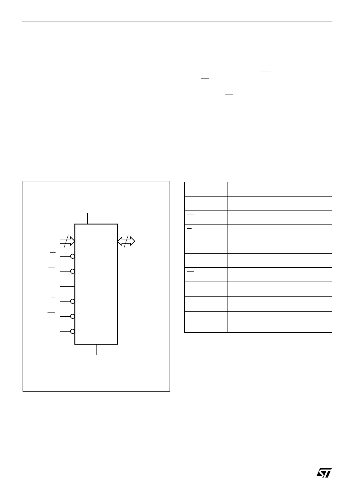
Figure 2. Logic Diagram Table 1. Signal Names
AI07260
20
A0-A19
W
DQ0-DQ15
V
CC
M69AR024B
G
16
E1
UB
LB
V
SS
E2
A0-A19 Address Inputs
DQ0-DQ15 Data Input/Output
E1
, E2 Chip Enable
G
Output Enable
W
Write Enable
UB
Upper Byte Enable Input
LB
Lower Byte Enable Input
V
CC
Supply Voltage
V
SS
Ground
NC
Not Connected
(no internal connection)
5/32
M69AR024B
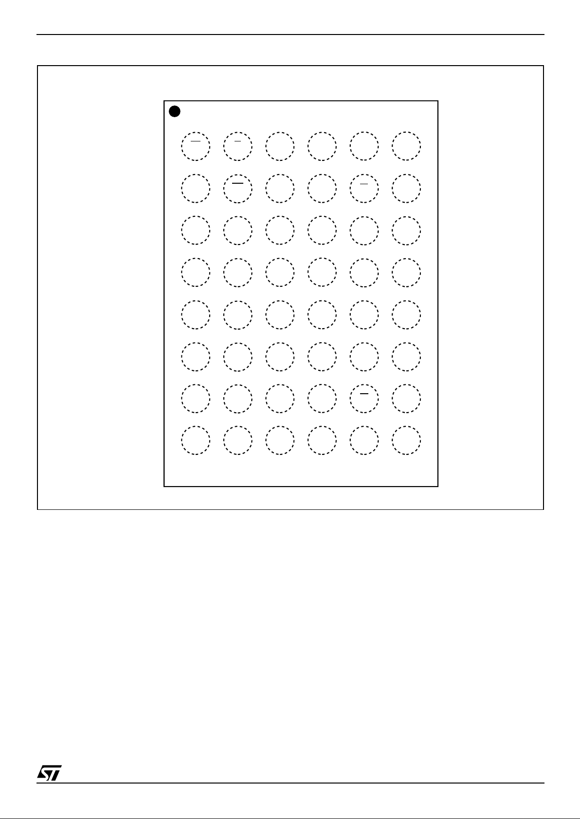
Figure 3. TFBGA Connections (Top view through package)
AI05861b
A
654321
E
B
F
A1
A0G
LB
A17
DQ7WA12
NCA11A8A18
DQ0A3
A6A5
A4 E1
A10
A9
A13
A7
A2 E2
C
DQ4
D
DQ5
A14
A15
G
H
DQ11
A19
UB
DQ10
DQ12
DQ13
V
SS
DQ15
DQ8
DQ9
DQ14
DQ3
DQ2DQ1
V
CC
V
CC
NC V
SS
DQ6
A16

M69AR024B
6/32
SIGNAL DESCRIPTIONS
See Figure 2, Logic Diagram, and Table 1, Sign al
Names, for a brief overview of the signals connected to this device.
Address Inputs (A0-A19). The Address Inputs
select the cell s in the memory arra y to access during Read and Write operations.
Data Inputs/Outputs (DQ8-DQ15). The Upper
Byte Data Inputs/Outputs carry the data to or from
the upper part of the selected address during a
Write or Read operation, when Upper Byte Enable
(UB
) is driven Low.
Data Inputs/Outputs (DQ0-DQ7). The Lower
Byte Data Inputs/Outputs carry the data to or from
the lower part of the selected address during a
Write or Read operation, when Lower Byte Enable
(LB
) is driven Low.
Chip Enable (E1
). When asserted (Low), the
Chip Enab le, E1
, activates the memory state machine, address buffers and decoders, allowing
Read and Write operations to be performed. When
de-asserted (High), all other pins are ignored, and
the device is put, automatically, in low-power
Standby mode.
Chip Enable (E2). The Chip Enable, E2, puts the
device in Deep Power-down mode when it
is driven Low. This is the lowest power mode.
Output Enable (G
). The Output Ena ble, G, pro-
vides a high speed tri-state control, allowing fast
read/write cycles to be achieved with the common
I/O data bus.
Write Enable (W
). The Write Enable, W, controls
the Bus Write operation of the memory’s Command Interface.
Upper Byte Enab le (UB
). The Upper Byte En-
able, UB
, gates the data on the Upper Byte Data
Inputs/Outputs (DQ8-DQ15) to or from the upper
part of the selected address during a Write or
Read operation.
Lower Byte Enable (LB
). The Lower Byte En-
able, LB
, gates the data on the Lower Byte Data
Inputs/Outputs (DQ0-DQ7) to or from the lower
part of the selected address during a Write or
Read operation.
V
CC
Supply Voltage. The VCC Supply Voltage
supplies the power for all operations (Read or
Write) and for driving the refresh logic, even when
the device is not being accessed.
Vss Ground. The V
SS
Ground is the reference
for all voltage measurements.
7/32
M69AR024B
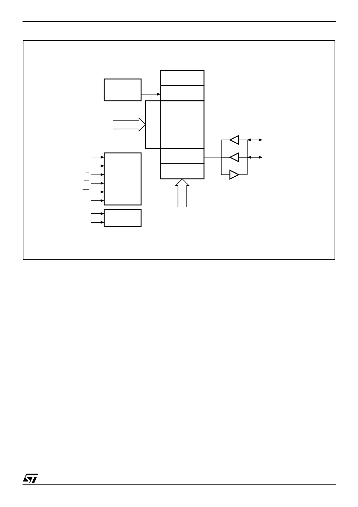
Figure 4. Blo ck Diagram
AI07261b
DYNAMIC
MEMORY
ARRAY
ROW DECODER
COLUMN
DECODER
CONTROL
LOGIC
E1
REFRESH
CONTROLLER
ARBITRATION
LOGIC
INTERNAL
CLOCK
GENERATOR
INPUT/OUTPUT
BUFFER
ADDRESS
UB
E2
G
W
LB
POWER
CONTROLLER
V
CC
V
SS
ADDRESS
DQ0-DQ7
DQ8-DQ15
M69AR024B
8/32
Table 2. Operating Modes
Note: 1. X = VIH or VIL.
2. Should not be kept in this logic condition longer than 1µs. Please contact your local ST sales office for the relaxation of 1µs limitation.
3. Power-d own mode c an be enter ed from the Standby s tate, and al l DQ pins are in High- Z state. I
PD
current and data retention de-
pend on the selection of Power Down Program. See "Power Down Program" for the detail.
4. Can be either VIL or VIH but must be valid before Read or Write.
Operation E2 E1 W G LB UB A0-A19 DQ0-DQ7 DQ8-DQ15
I
CC
Data Re-
tention
Standby
(Deselect)
V
IH
V
IH
X
(1)
X
(1)
X
(1)X (1)
X
(1)
Hi-Z Hi-Z
I
SB
Yes
Output Disabled
V
IH
V
IL
V
IH
V
IH
X
(1)X (1)
Note
(4)
Hi-Z Hi-Z
I
CC
Yes
Output Disabled
(No Read)
(2)
V
IH
V
IL
V
IH
V
IL
V
IH
V
IH
Valid Hi-Z Hi-Z
I
CC
Yes
Upper Byte
Read
(2)
V
IH
V
IL
V
IH
V
IL
V
IH
V
IL
Valid Hi-Z
Output
Valid
I
CC
Yes
Lower Byte
Read
(2)
V
IH
V
IL
V
IH
V
IL
V
IL
V
IH
Valid
Output
Valid
Hi-Z
I
CC
Yes
Word Read
(2)
V
IH
V
IL
V
IH
V
IL
V
IL
V
IL
Valid
Output
Valid
Output
Valid
I
CC
Yes
No Write
(2)
V
IH
V
IL
V
IL V
IH
V
IH
V
IH
Valid Invalid Invalid
I
CC
Yes
Upper Byte
Write
(2)
V
IH
V
IL
V
IL
V
IH
V
IH
V
IL
Valid Invalid Input Valid
I
CC
Yes
Lower Byte
Write
(2)
V
IH
V
IL
V
IL
V
IH
V
IL
V
IH
Valid Input Valid Invalid
I
CC
Yes
Word Write
(2)
V
IH
V
IL
V
IL
V
IH
V
IL
V
IL
Valid Input Valid Input Valid
I
CC
Yes
Power-down
(3)
V
IL
X
(1)X (1)
X
(1)
X
(1)X (1)
X
(1)
Hi-Z Hi-Z
I
PD
Yes/No

9/32
M69AR024B
OPERATION
Operational modes are determined by device control in puts W
, E1, E2, LB and U B as summarized
in the Operating Modes table (see Table 2).
Power On Se quence
Because the internal control logic of the
M69AR024B needs to be initialized, the following
power-on procedure must be followed before the
memory is used:
– Apply power and wait for V
CC
to stabilize
– Wait 300µs while driving both Chip Enable
signals (E1
and E2) High
Read Mode
The device is in Read mode when:
– Write Enable (W
) is High and
– Output Enable (G
) Low and
– Upper Byte Enable (UB
) or Lower Byte En-
able (LB
) is Low, or both
– the two Chip Enable signals are asserted (E1
is Low, and E2 is High).
The time taken to enter Read mode (t
ELQV
, t
GLQV
or t
BLQV
) depends on which of the above signals
was the last to reach the appropriate level.
Data out (DQ15-DQ0) may be indeterminate
during t
ELQX
, t
GLQX
and t
BLQX
, but data will always
be valid during t
AVQV
.
Write Mode
The device is in Write mode when
– Write Enable (W
) is Low and
– Chip Enable (E1
) is Low and
– Upper Byte Enable (UB
) or Lower Byte En-
able (LB
) is Low, or both
– the two Chip Enable signals are asserted (E1
is Low, and E2 is High).
The Write cycle begins just after the event (the falling edge) that causes the last of these conditions
to become true (t
AVWL
or t
AVEL
or t
AVBL
).
The Write cycle is terminated by the earlier of a rising edge on Write Enable (W
) or Chip Enable (E1).
If the device is in Write mode (Chip Enable (E1
) is
Low, Output Enable (G
) is Low, Upp er Byte En-
able (UB
) or Lower Byte Enable (LB) is Low), then
Write Enable (W
) will return the outputs to high im-
pedance within t
WLQZ
of its falling edge. Care must
be taken to avoid bus contention in this type of operation. Data input must be valid for t
DVWH
before
the rising edge of Wr ite Enable (W
), or for t
DVEH
before the rising edge of Chip Enable (E1), whichever occurs first, and remain valid for t
WHDX
, t
EHDX
Standby Mode
The device is in Standby mode when:
– Chip Enable (E1
) is High and
– Chip Enable (E2) is High
The input/output buffers and t he decoding/c ontrol
logic are switched off, but the dynamic array continues to be refreshed. In this mode, the me mory
current consumption, I
SB
, is reduced, and the data
remains valid.
Deep Power-down Mode
The device is in Deep Power-down mode when:
– Chip Enable (E2) is Low
M69AR024B
10/32
MAXIMUM RA TING
Stressing the de vice above the rating l isted in t he
“Absolute Maximum Ratings" table may cause
permanent damage to the device. These are
stress ratings only and operation of t he device at
these or any other conditions above those indicat-
ed in the Operating sections of this specification is
not implied. Exposure to Abs olute M aximum Ra ting conditions for extended periods may affect device r eliab ilit y.
Table 3. Absolute Maximum Ratings
Note: 1. The mi nimum DC voltage on input or I/O pi ns is –0.3 V. During voltage transi tions, inputs may und ershoot V
SS
by 1.0V f or periods
of up to 5ns.
2. The maxim um DC volta ge on inpu t and I/O pins is V
CC
+0.2V. During voltage transitions, inputs may overshoot VCC by 1.0V fo r
periods of up to 5ns.
Symbol Parameter Min Max Unit
I
O
Output Current –50 50 mA
T
A
Ambient Operating Temperature –25 85 °C
T
STG
Storage Temperature –55 125 °C
V
CC
Core Supply Voltage –0.2 3.3 V
V
IO
(1,2)
Input or Output Voltage –0.2 3.3 V
 Loading...