

4 Mbit (512Kb x8) Low Power SRAM with Output Enable
■ ULTRA LOW DATA RETENTION CURRENT
– 100nA (typical)
–10µA (max)
■OPERATION VOLTAGE: 5V ±10%
■ 512 Kbit x8 SRAM with OUTPUT ENABLE
■ EQUAL CYCLE and ACCESS TIMES: 70ns
■ LOW V
■ TRI-STATE COMMON I/O
■ CMOS for OPTIMUM SPEED/POWER
■ AUTOMATIC POWER-DOWN WHEN
DESELECTED
■ INTENDED FOR USE WITH ST
ZEROPOWER
CONTROLLERS
DATA RETENTION: 2V
CC
®
AND TIMEKEEPER®
M68Z512
32
1
TSOP II 32 (NC)
10 x 20mm
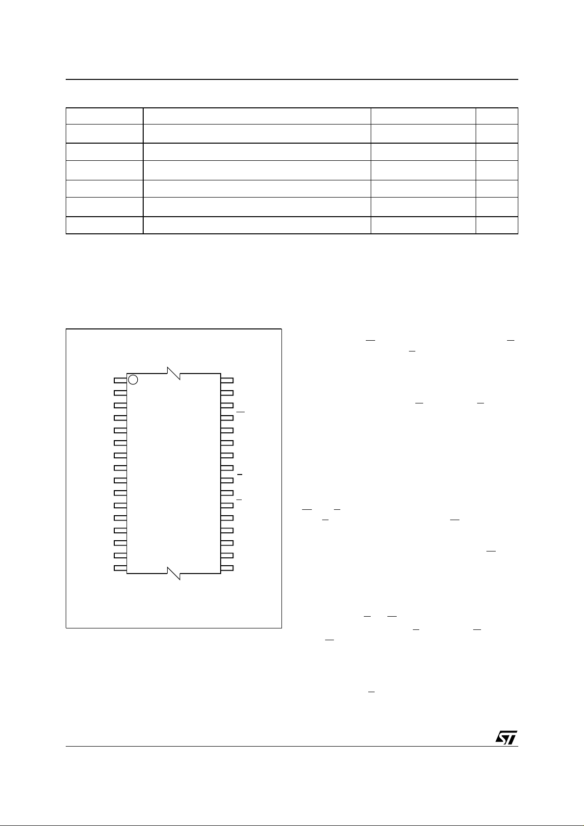
Figure 1. Logic Diagram
DESCRIPTION
The M68Z512 is a 4 Mbit (4,194,304 bit) CMOS
SRAM, organized as 524,288 words by 8 bits. The
device features fully static operat ion requiring no
external clocks or timing strobes, with equal address access and cycle times. It requires a single
5V ±10% supply, and all inputs and outputs are
TTL compatible.
This device has an automatic power-down feature,
reducing the power consumption by over 99%
when deselected.
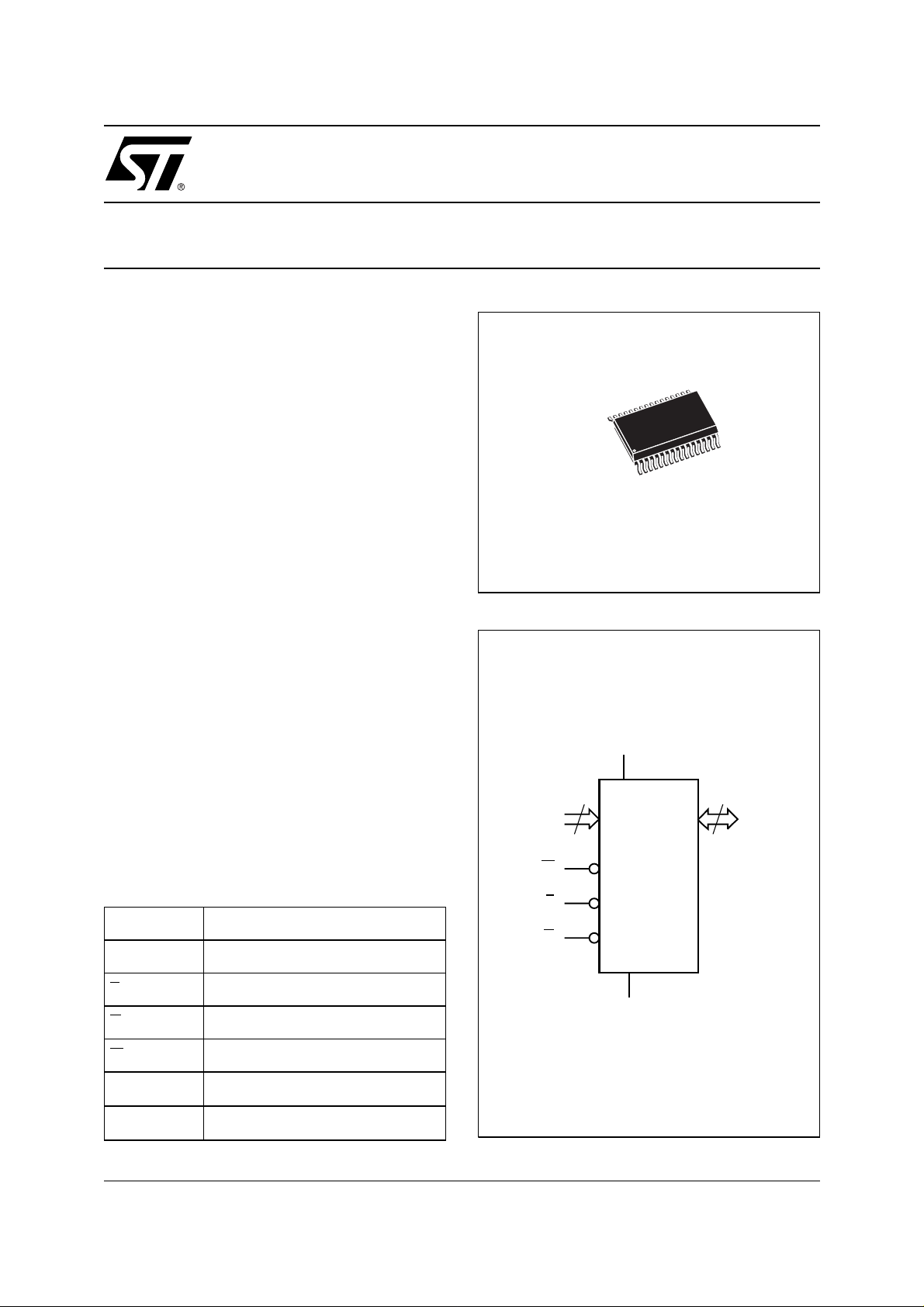
The M68Z512 is a vailable in a 32 lea d TSOP II
(10 x 20mm) package.
Table 1. Signal Names
A0-A18 Address Inputs
DQ0-DQ7 Data Input/Output
E
G
W
V
CC
Chip Enable
Output Enable
Write Enable
Supply Voltage
A0-A18
W
V
CC
19
M68Z512
E
G
V
SS
8
DQ0-DQ7
AI03030
V
SS
Ground
1/12March 2000
M68Z512
Table 2. Absolute Maximum Ratings
Symbol Parameter Value Unit
T
A
T
STG
(2)
V
IO
V
CC
(3)
I
O
P
D
Note: 1. Ex cept for the rating "Operati ng Temperat ure Range" , stresses above th ose listed i n the Tab l e "Absolute Maximum Ratings" may
cause permanent damage to the device. These are stress ratings only and operation of the device at these or any other conditions
above those indi cated in the Operating sections of this s pecification is not impli ed. Exposure to Absolute M aximum Rating conditions for extended per iods may aff ect device reliabilit y. Refer also to the STMicroel ectronics SURE Program an d other relevan t qual ity docum en ts .
2. Up to a maxim um operatin g V
3. One output at a tim e, not to exceed 1 secon d duration.
Ambient Operating Temperature
Storage Temperature –65 to 150 °C
Input or Output Voltage
Supply Voltage –0.3 to 7.0 V
Output Current 20 mA
Power Dissipation 1 W
of 5.5V only.
CC
Figure 2. TSOP Connection s
(1)
READ MODE
0 to 70 °C
–0.3 to V
CC
+ 0.3
V
The M68Z512 is in the Read mode whenever
Write Ena ble (W
Low, and Chip Enable (E
) is High with Output Enable (G)
) is asserted. This pro-
vides access to data from e ight of the 4,194,304
A17
A16
A14
A12
A7
A6
A5
A4
A3
A2
A1
A0
DQ0
DQ1
DQ2
V
SS
1
8
9
M68Z512
32
25
24
16 17
AI03031
V
CC
A15
A18
W
A13
A8
A9
A11
G
A10
E
DQ7
DQ6
DQ5
DQ4
DQ3
locations in the static memory array, specified by
the 19 address inputs. Valid data wil l be availa ble
at the eight output pins within t
stable address, providing G
is Low and E is Low.
after the last
AVQV
If Chip Enable or Output Enable access times are
not met, data access will be measured from the
limiting parameter (t
address. Data out may be indeterminate at t
and t
t
AVQV
, but data lines will always be valid at
GLQX
.
ELQV
or t
) rather than the
GLQV
ELQX
WRITE MODE
The M68Z512 is in the Write mode whenever the
and E pins are Low. Either the Chip Enable in-
W
put (E
) or the Write E nabl e i nput (W) must be deasserted during Address transitions for subsequent write cycles. Write begins with the concurrence of Chip Enable being active with W
low.
Therefore, address setup time is referenced to
Write Enable and Chip Enable as t
AVWL
and t
AVEH
respectively, and is determined by the latter occurring edge.
The Write cycle can be terminated by the earlier
rising edge of E
if the Output is enabled (E
then W
within t
will return the outputs to high impedance
WLQZ
, or W.
= Low and G = Low),
of its falling edge. Care must be taken
to avoid bus c ontention in this type of operation.
Data input must be valid for t
ing edge of Write Enable, or for t
rising edge of E
main v a lid for t
, whichever occurs first, and re-
or t
WHDX
EHDX
before the ris-
DVWH
DVEH
.
before the
2/12
Table 3. Operating Modes
Operation E W G DQ0-DQ7 Power
Read
Read
Write
Deselect
Note: 1. X = VIH or VIL.
M68Z512
V
IL
V
IL
V
IL
V
IH
V
IH
V
IH
V
IL
X
V
IH
V
IL
Hi-Z Active
Data Output Active
X Data Input Active
X
Hi-Z Standby
Table 4. AC Measurement Conditions
Input Rise and Fall Times ≤ 5ns
Figure 3. AC Testing Load Circuit
5.0V
Input Pulse Voltages 0 to 3V
Input and Output Timing Ref. Voltages 1.5V
Note: Output Hi -Z is de fin ed as the po int whe re data is no l onge r
driven.
OPERATIONAL MODE
The M68Z512 has a Chip Enable power down feature which invokes an automatic standby mode
whenever Chip Enable is de-as serted (E
An Output Enable (G
) signal provides a high
= High).
DEVICE
UNDER
TEST
994Ω
1838Ω
OUT
CL = 100pF or 5pF
speed tri-state control, allowing fast read/write cycles to be achieved with the common I/O data bus.
Operational modes are determined by device control inputs W
and E as summarized in the Ope ra t-
CL includes JIG capacitance
AI03032
ing Modes table.
Table 5. Capacitance
Symbol Parameter Test Condition Min Max Unit
C
C
OUT
Note: 1. Sampled only, not 100% tested.
Input Capacitance on all pins (except DQ)
IN
(2)
Output Capacitanc e
2. Outputs desel ected.
(1)
(TA = 25°C, f = 1 MHz)
T
= 25°C, f = 1MHz, VCC = 5V
A
T
= 25°C, f = 1MHz, VCC = 5V
A
6pF
8pF
3/12
M68Z512
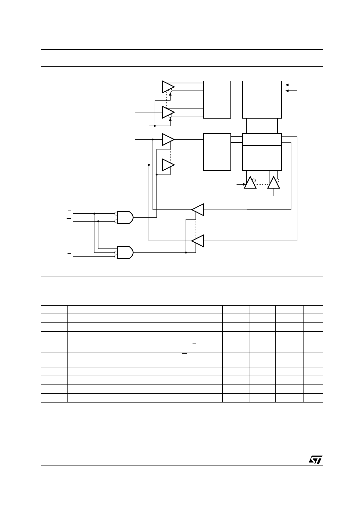
Figure 4. Block Diagram
A
A
CHIP ENABLE.
(10)
ROW
DECODER
MEMORY
ARRAY
V
CC
V
SS
DQ
(8)
DQ
E
W
G
INPUT
DATA
CTRL
CHIP ENABLE.
I/O CIRCUITS
COLUMN
DECODER
(9)
A A
AI03033
Table 6. DC Characteristics
(T
= 0 to 70°C; VCC = 5V ±10%)
A
Symbol Parameter Test Condition Min Typ Max Unit
I
Input Leakage Current
LI
I
I
CC1
I
CC2
I
CC3
V
V
V
V
Note: 1. Av erage AC cu rrent, Outputs open, cyc l i ng at t
Output Leakage Current
LO
(1)
Supply Current
(2)
Supply Current (Standby) TTL
(3)
Supply Current (Standby) CMOS
Input Low Voltage –0.3 0.8 V
IL
Input High Voltage 2.2
IH
Output Low Voltage
OL
Output High Voltage
OH
2. All other Inputs at V
3. All other Inputs at V
≤ 0.8V or VIH ≥ 2.2V.
IL
≤ 0.3V or VIH ≥ VCC –0.3V.
IL
0V ≤ V
0V
V
V
CC
= 5.5V, E ≥ V
V
CC
minimum.
AVAV
≤ V
IN
CC
≤ V
≤ V
OUT
= 5.5V, (-55)
CC
= 5.5V, E = VIH
CC
f=0
I
= 2.1mA
OL
I
= –1mA
OH
CC
– 0.3V,
±1 µA
±1 µA
90 mA
15 mA
1.6 20 µA
V
+ 0.3
CC
0.4 V
2.4 V
V
4/12
 Loading...