

SGS Thomson Microelectronics M68Z128W Datasheet
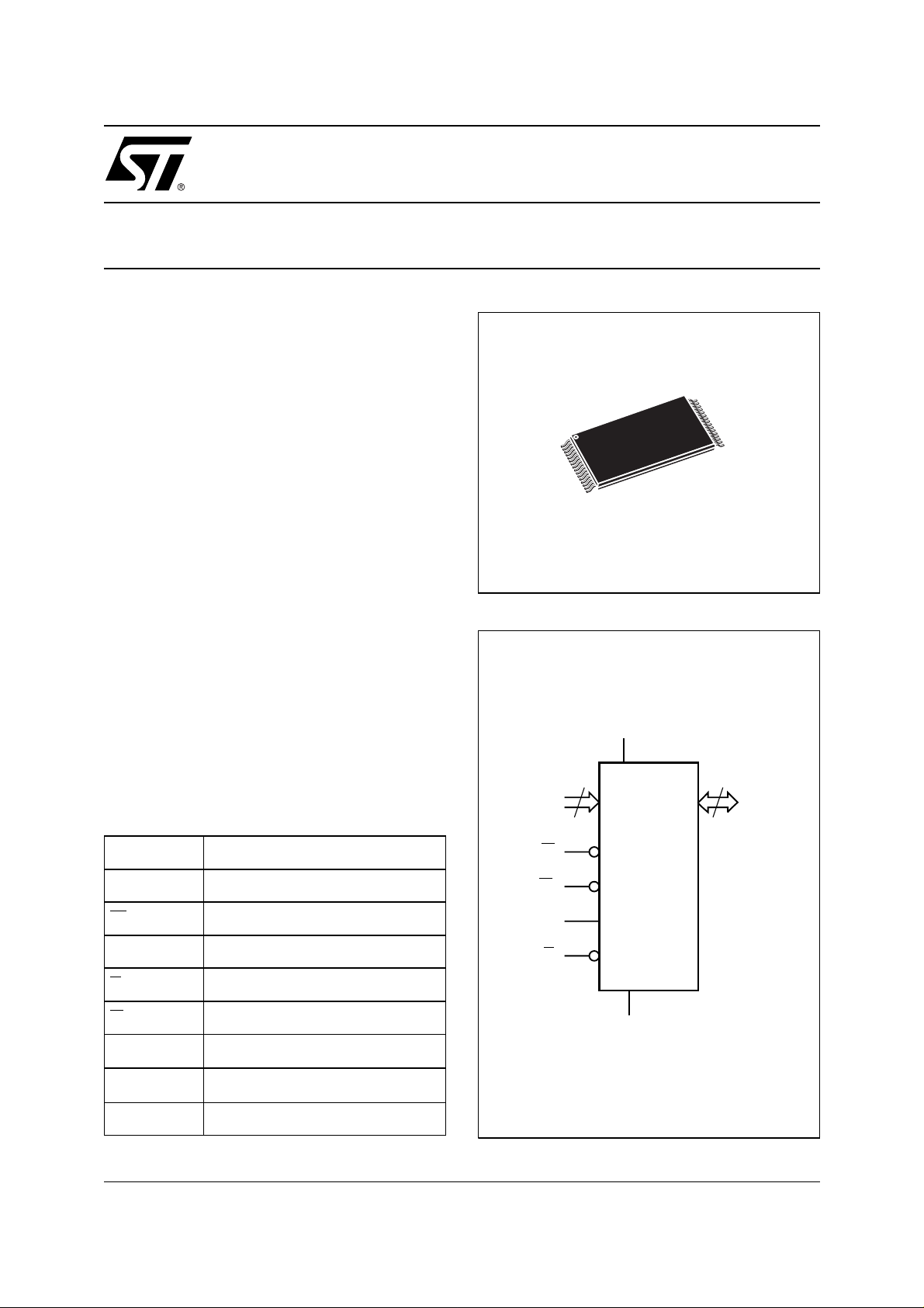
M68Z128W
3V, 1 Mbit (128Kb x8) Low Power SRAM with Output Enable
■ LOW VOLTAGE: 3.0V (+0.6V / –0.3V)
■ 128Kb x 8 LOW POWER SRAM with OUTPUT
ENABLE
■ EQUAL CYCLE and ACC ESS TIMES: 70ns
■ LOW V
■ TRI-STATE COMMON I/O
■ LOW ACTIVE and STAN DB Y POWER
■ INTENDED for USE with ST ZEROPOWER
and TIMEKEEPER
DESCRIPTION
The M68Z128W is a 1 Mbit (1,048,576 bi t) Fast
CMOS SRAM, organized as 131,072 words by 8
bits. The device features fully static opera tion requiring no external clocks or timing strobes, with
equal address access and cycle times. It requires
a single 3.0V (+0.6V / –0.3V) supply, and all inputs
and outputs are TTL compatible. This device has
an automatic power-down feature, reducing the
power consumption by over 99% when desel ected. The M68Z128 W is available in the sta ndard
450mil-wide TSOP type 1 package.
DATA RETENTION: 1.4V
CC
®
CONTROLLERS
®
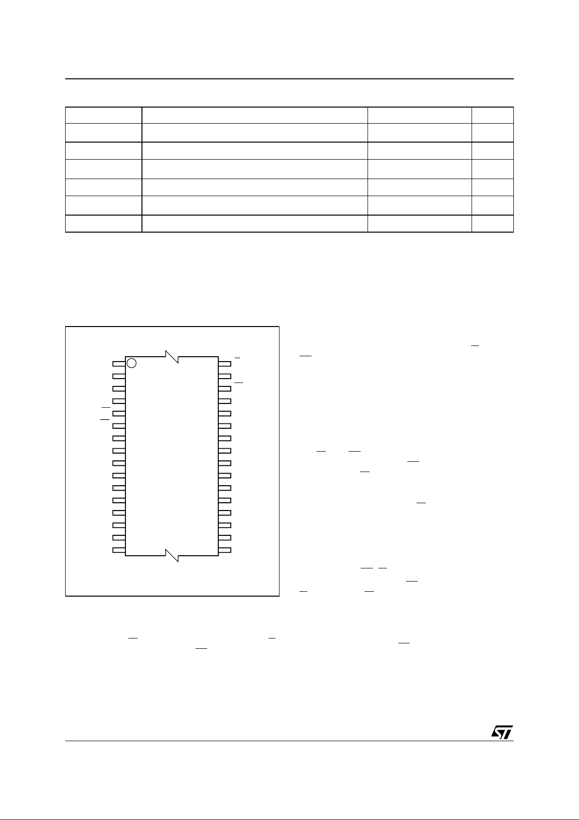
TSOP32 (N)
8 x 20mm
Figure 1. Logic Diagram
V
CC
Table 1. Signal Names
A0-A16 Address Inputs
DQ0-DQ7 Data Input/Output
E1
E2 Chip Enable 2
G
W
V
CC
V
SS
NC Not Connected Internally
Chip Enable 1
Output Enable
Write Enable
Supply Voltage
Ground
A0-A16
W
E1
E2
17
M68Z128W
G
V
SS
8
DQ0-DQ7
AI01878B
1/12March 2000
M68Z128W
Table 2. Absolute Maximum Ratings
Symbol Parameter Value Unit
T
A
T
STG
(2)
V
IO
V
CC
(3)
I
O
P
D
Note: 1. Except for the ratin g " Operati ng Temperat ure Range" , stresses above th ose listed i n the Tab l e "Absolute Maximum Ratings" may
cause permanent damage to the device. These are stress ratings only and operation of the device at these or any other conditions
above those indi cated in the Operating sections of this s pecification is not i mplied. Exposu re to Ab solute Ma xi m um Rati ng conditions for extended per iods may aff ect device reliabilit y. Refer also to the STMicroel ectronics SURE Program an d other relevan t qual ity docum en ts .
2. Up to a m aximum op erating V
3. One out put at a time, not to exceed 1 s econd durat i on.
Ambient Operating Temperature
Storage Temperature –65 to 150 °C
Input or Output Voltage
Supply Voltage –0.5 to 4.6 V
Output Current 20 mA
Power Dissipation 1 W
of 3.6V only.
CC
Figure 2. TSOP Connection s
(1)
0 to 70 °C
–0.5 to V
CC
+ 0.5
V
the 1,048,576 locations in the static memory array,
specified by the 17 address inputs. Val id dat a wi ll
be available at the eight output pins within t
AVQV
after the last stable address, providing G is Low,
is Low and E2 is High. If Chip Enable or Output
A11 G
1
A9
A8
A13
W
E2
A15
V
CC
NC
8
9
M68Z128W
A16
A14
A12
A7
A6
A5
A4 A3
16 17
32
25
24
AI00698B
A10
E1
DQ7
DQ6
DQ5
DQ4
DQ3
V
SS
DQ2
DQ1
DQ0
A0
A1
A2
READ MODE
The M68Z128W is in the Read mode whenever
Write Ena ble (W
Low, and both Chip Enables (E1
) is High with Output Enable (G)
and E2) are as-
serted. This provides acc ess to dat a fr om eight of
E1
Enable access times are not met, data access will
be measured from the limiting parameter (t
E2HQV
, or t
t
may be indeterminate at t
) rather than the address. Data out
GLQV
E1LQX
, t
E2HQX
but data lines will always be valid at t
and t
AVQV
E1LQV
GLQX
.
WRITE MODE
The M68Z128W is in the Write mode whenever
and E1 pins are Lo w, with E2 High. Either
the W
the Chip Enable input s (E1
Enable input (W
) must be de-asserted during Ad-
and E2) or the Write
dress transitions for subsequent write cycles.
Write begins with the concurrence of both Chip
Enables being active with W
low. Therefore, address setup time is r eferenced to Write Enable and
both Chip Enables as t
AVWL
, t
AVE1L
and t
AVE2H
respectively, and is determined by the latter occurring edge.
The Write cycle can be terminated by the earlier
rising edge of E1
If the Output is enabled (E1
= Low), then W will return the outputs to high im-
G
pedance within t
, W, or the falling edge of E2.
= Low, E2 = High and
of its falling edge. Care must
WLQZ
be taken to avoid bus contention in this type of operation. Data input must be valid for t
the rising edge of Write E nable, o r for t
fore the rising edge of E1
or for t
DVE2L
before
DVWH
DVE1H
before the
be-
falling edge of E2, whi chever occurs f irst, and remain v a lid for t
WHDX
, t
E1HDX
or t
E2LDX
.
,
,
2/12
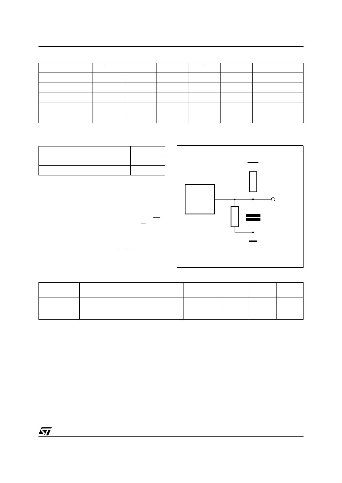
Table 3. Operating Modes
Operation E1 E2 W G DQ0-DQ7 Power
Read
Read
Write
Deselect
Deselect X
Note: 1. X = VIH or VIL.
V
IL
V
IL
V
IL
V
IH
V
IH
V
IH
V
IH
V
IH
V
IH
V
IL
XX
V
IL
X
V
IH
V
IL
X
Data Output
Data Input Active
X
X
Hi-Z Active
Hi-Z Standby
Hi-Z Standby
M68Z128W
Active
Table 4. AC Measurement Conditions
Input Rise and Fall Times ≤ 15ns
Input Pulse Voltages 0 to 3V
Input and Output Timing Ref. Voltages 1.5V
Note: O ut put H i-Z is defin ed as t he poi nt w here da ta is no lo nger
driven.
OPERATIONAL MODE
The M68Z128W has a Chip Enable power down
feature which invokes an automatic standby mode
whenever either Chip Enable is de-asserted (E1
High or E2 = Low). An Output Enable (G
=
) signal
provides a high speed tri-state control, allowing
fast read/write cycles to be achieved with the common I/O data bu s. Operational mo des are determined by device control inputs W
, E1, and E2 as
summarized in the Operating Modes table.
Table 5. Capacitance
Symbol Parameter
C
IN
(2)
C
OUT
Note: 1. Sampled only, not 100% tested.
2. Outputs deselected.
(1)
(TA = 25 °C, f = 1 MHz)
Input Capacitance on all pins (except DQ)
Output Capacitance
Figure 3. AC Testing Load Circuit
3.3V
1213Ω
DEVICE
UNDER
TEST
1378Ω
CL includes JIG capacitance
Test
Condition
V
= 0V
IN
V
= 0V
OUT
Min Max Unit
CL = 50pF or 5pF
6pF
8pF
OUT
AI00697
3/12
M68Z128W
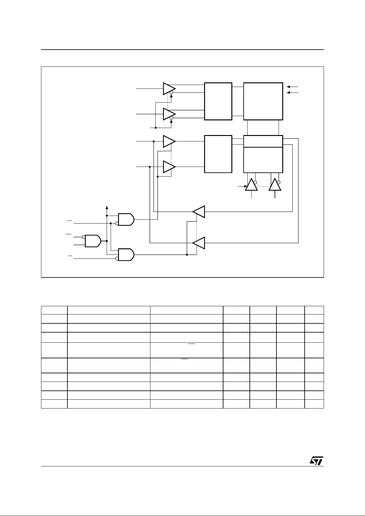
Figure 4. Block Diagram
A
A
CHIP ENABLE.
(9)
ROW
DECODER
MEMORY
ARRAY
V
CC
V
SS
E1
E2
DQ
(8)
DQ
CHIP
ENABLE
W
G
INPUT
DATA
CTRL
CHIP ENABLE.
I/O CIRCUITS
COLUMN
DECODER
(8)
A A
AI00665
Table 6. DC Characteristics
(T
= 0 to 70°C; VCC = 3.0V + 0.6V / –0.3V)
A
Symbol Parameter Test Condition Min Typ Max Unit
I
Input Leakage Current
LI
I
I
CC1
I
CC2
I
CC3
V
V
V
V
Note: 1. Average AC current, Ou tputs open, c ycling at t
Output Leakage Current
LO
(1)
Supply Current
(2)
Supply Current (Standby) TTL
(3)
Supply Current (Standby) CMOS
Input Low Voltage –0.5 0.8 V
IL
Input High Voltage 2
IH
Output Low Voltage
OL
Output High Voltage
OH
2. All other Inputs at V
3. All other Inputs at V
≤ 0.8V or VIH ≥ 2.0V.
IL
≤ 0.2V or VIH ≥ VCC –0.2V.
IL
0V ≤ V
0V
V
V
CC
= 3.6V , E1 ≥ V
V
CC
or E2 ≤ 0.2V, f =0
minimum.
AVAV
≤ V
IN
CC
≤ V
≤ V
OUT
= 3.6V, (-70)
CC
CC
= 3.6V, E1 = VIH or
E2 = V
I
I
= 2.1mA
OL
= –1mA
OH
IL
, f =0
CC
– 0.2V
±1 µA
±1 µA
20 40 mA
15 300 µA
0.4 15 µA
V
+ 0.5
CC
0.4 V
2.4 V
V
4/12
 Loading...