

SGS Thomson Microelectronics M68AW512D Datasheet
8 Mbit (512K x16) 3.0V Asynchronous SRAM
FEATURES SUMMARY
■ SUPPLY VOLTAGE : 2.7 to 3.6V
■ 512K x 16 bits SRAM with OUTPUT ENABLE
■ EQUAL CYCLE and ACCESS TIMES: 55, 70ns
■ LOW STANDBY CURRENT
■ LOW V
■ TRI-STATE COMMON I/O
■ AUTOMATIC POWER DOWN
DATA RETENTION: 1.5V
CC
M68AW512D
Figure 1. Packages
BGA
TFBGA48 (ZB)
8 x 10 mm
1/18November 2002

M68AW512D
TABLE OF CONTENTS
SUMMARY DESCRIPTION . . . . . . . . . . . . . . . . . . . . . . . . . . . . . . . . . . . . . . . . . . . . . . . . . . . . . . . . . . 3
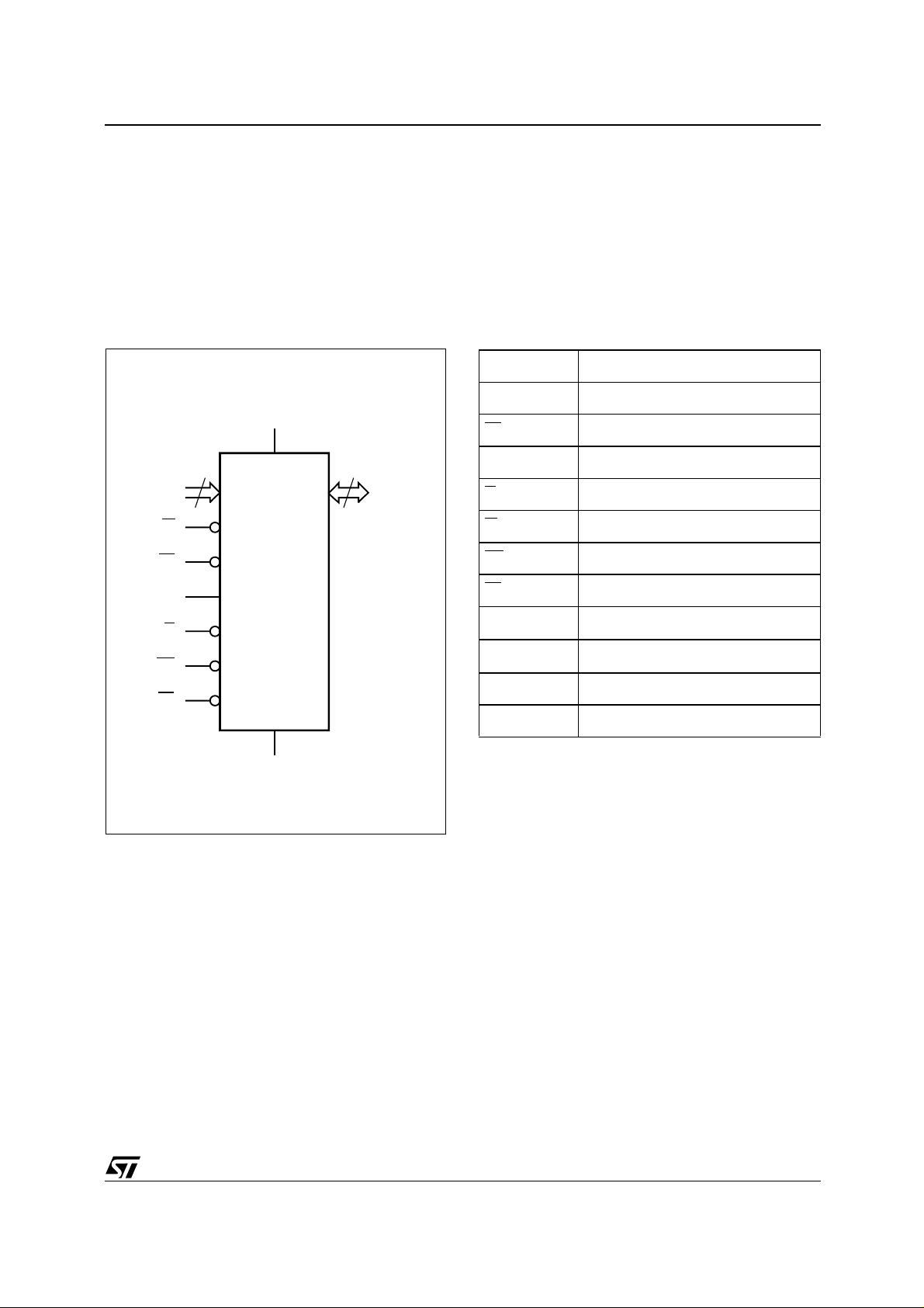
Figure 2. Logic Diagram . . . . . . . . . . . . . . . . . . . . . . . . . . . . . . . . . . . . . . . . . . . . . . . . . . . . . . . . . . 3
Table 1. Signal Names . . . . . . . . . . . . . . . . . . . . . . . . . . . . . . . . . . . . . . . . . . . . . . . . . . . . . . . . . . . 3
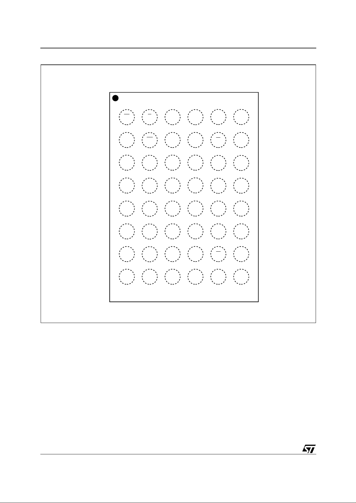
Figure 3. TFBGA Connections (Top view through package). . . . . . . . . . . . . . . . . . . . . . . . . . . . . . . 4
Figure 4. Block Diagr am . . . . . . . . . . . . . . . . . . . . . . . . . . . . . . . . . . . . . . . . . . . . . . . . . . . . . . . . . . 5
MAXIMUM RATING . . . . . . . . . . . . . . . . . . . . . . . . . . . . . . . . . . . . . . . . . . . . . . . . . . . . . . . . . . . . . . . . 5
Table 2. Absolute Maximum Ratings. . . . . . . . . . . . . . . . . . . . . . . . . . . . . . . . . . . . . . . . . . . . . . . . . 5
DC and AC PARAMETERS. . . . . . . . . . . . . . . . . . . . . . . . . . . . . . . . . . . . . . . . . . . . . . . . . . . . . . . . . . 6
Table 3. Operating and AC Measurement Conditions. . . . . . . . . . . . . . . . . . . . . . . . . . . . . . . . . . . . 6
Figure 5. AC Measurement I/O Waveform . . . . . . . . . . . . . . . . . . . . . . . . . . . . . . . . . . . . . . . . . . . . 6
Figure 6. AC Measurement Load Circuit . . . . . . . . . . . . . . . . . . . . . . . . . . . . . . . . . . . . . . . . . . . . . .6
Table 4. Capacitance. . . . . . . . . . . . . . . . . . . . . . . . . . . . . . . . . . . . . . . . . . . . . . . . . . . . . . . . . . . . . 7
Table 5. DC Character i stics. . . . . . . . . . . . . . . . . . . . . . . . . . . . . . . . . . . . . . . . . . . . . . . . . . . . . . . . 7
OPERATION. . . . . . . . . . . . . . . . . . . . . . . . . . . . . . . . . . . . . . . . . . . . . . . . . . . . . . . . . . . . . . . . . . . . . . 8
Table 6. Operating Modes. . . . . . . . . . . . . . . . . . . . . . . . . . . . . . . . . . . . . . . . . . . . . . . . . . . . . . . . . 8
Read Mode . . . . . . . . . . . . . . . . . . . . . . . . . . . . . . . . . . . . . . . . . . . . . . . . . . . . . . . . . . . . . . . . . . . . 8
Figure 7. Address Controlled, Read Mode AC Waveforms. . . . . . . . . . . . . . . . . . . . . . . . . . . . . . . . 8
Figure 8. Chip Enable or Output Enable Controlled, Read Mode AC Waveforms . . . . . . . . . . . . . . 9
Figure 9. Chip Enable or UB/LB Controlled, Standby Mode AC Waveforms . . . . . . . . . . . . . . . . . . 9
Table 7. Read and Standby Mode AC Characteristics . . . . . . . . . . . . . . . . . . . . . . . . . . . . . . . . . . 10
Write Mode . . . . . . . . . . . . . . . . . . . . . . . . . . . . . . . . . . . . . . . . . . . . . . . . . . . . . . . . . . . . . . . . . . . 11
Figure 10. Write En a ble Controlled, Write AC Waveforms . . . . . . . . . . . . . . . . . . . . . . . . . . . . . . . 11
Figure 11. Chip Enable Controlled, Write AC Waveforms. . . . . . . . . . . . . . . . . . . . . . . . . . . . . . . . 12
Figure 12. UB/LB Controlled, Write AC Waveforms . . . . . . . . . . . . . . . . . . . . . . . . . . . . . . . . . . . . 12
Table 8. Write Mode AC Characteristics . . . . . . . . . . . . . . . . . . . . . . . . . . . . . . . . . . . . . . . . . . . . . 13
Figu r e 1 3 . E1 Con trolled, Lo w VCC Data R e t e n tion A C Wav e fo r ms . . . . . . . . . . . . . . . . . . . . . . . 14
Figu r e 1 4 . E2 Cont r o l led, Lo w VCC Da ta R e tent io n AC Wav e fo r ms . . . . . . . . . . . . . . . . . . . . . . . 14
Table 9. Low VCC Data Retention Characteristics . . . . . . . . . . . . . . . . . . . . . . . . . . . . . . . . . . . . . 14
PACKAGE MECHANICAL . . . . . . . . . . . . . . . . . . . . . . . . . . . . . . . . . . . . . . . . . . . . . . . . . . . . . . . . . . 15
TFBGA48 8x10mm - 6x8 ball array, 0.75 mm pitch, Bottom View Package Outline. . . . . . . . . . . . 15
TFBGA48 8x10mm - 6x8 ball array, 0.75 mm pitch, Package Mechanic al Data . . . . . . . . . . . . . . . 15
PART NUMBERING. . . . . . . . . . . . . . . . . . . . . . . . . . . . . . . . . . . . . . . . . . . . . . . . . . . . . . . . . . . . . . . 16
Table 11. Ordering Information Scheme . . . . . . . . . . . . . . . . . . . . . . . . . . . . . . . . . . . . . . . . . . . . . 16
REVISION HISTORY . . . . . . . . . . . . . . . . . . . . . . . . . . . . . . . . . . . . . . . . . . . . . . . . . . . . . . . . . . . . . . 17
Table 12. Document Revision History. . . . . . . . . . . . . . . . . . . . . . . . . . . . . . . . . . . . . . . . . . . . . . .17
2/18
SUMMARY DESCRIPTION
The M68AW512D is an 8 Mbit (8,388,608 bit)
CMOS SRAM, organized as 524,288 words by 16
bits. The device features fully static operation requiring no external clocks or timing strobes, with
equal address access and cycle times. It requires
a single 2.7 to 3.6V supply. This device has a Chip
it is active (E2 high) the device has an auto matic
power-down feature, reducing the power consumption by over 99%.
The M68AW512D is available in TFBGA48 (0.75
mm ball pitch) package.
Select pin (E2) for easy memory expansion; when
Figure 2. Logic Diagram Table 1. Signal Names
A0-A18 Address Inputs
DQ0-DQ15 Data Input/Output
V
CC
E1
Chip Enable
M68AW512D
A0-A18
W
E1
E2
UB
LB
19
16
DQ0-DQ15
M68AW512D
G
V
SS
AI04800b
E2 Chip Select
G
W
UB
LB
V
CC
V
SS
NC Not Connected
DU Don’t Use as Internally Connected
Output Enable
Write Enable
Upper Byte Enable Input
Lower Byte Enable Input
Supply Voltage
Ground
3/18
M68AW512D
Figure 3. TFBGA Connections (Top view through package)
654321
A
B
C
D
E
F
G
H
DQ8
DQ9
V
SS
V
CC
DQ14
DQ15
UB
DQ10
DQ11
DQ12
DQ13
NC
A0GLB
A17
V
A14
A9
SS
A1
A4 E1
A6A5
A7
A16
A15
A13
A10
A2 E2
DQ3
DQ4
DQ5
DQ0A3
DQ2DQ1
V
CC
V
SS
DQ6
DQ7WA12
DUA11A8A18
4/18
AI03960
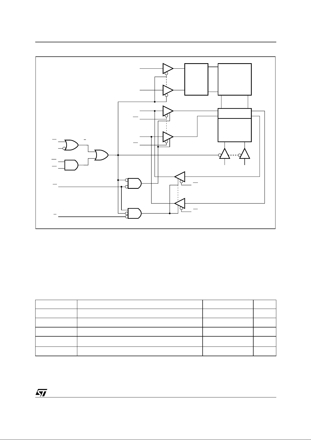
Figure 4. Block Diagram
A18
A8
ROW
DECODER
M68AW512D
MEMORY
ARRAY
DQ15
UB
E1
E2
UB
LB
Ex
W
G
DQ0
LBLB
MAXIMUM RATI N G
Stressing the device above the rating l isted in t he
Absolute Maximum Ratings" table may cause permanent damage to the device. These are stress
ratings only and operation of the device at t hese or
any other conditions ab ove those i ndicated in t he
Operating sections of this specificat ion is not im-
(8)
(8)
(8)
UB
(8)
LB
I/O CIRCUITS
COLUMN
DECODER
A0 A7
AI05452
plied. Exposure to Absolute Maximum Rating conditions for periods greater than 1 sec may affect
device reliability. Refer also to the STMicroelectronics SURE Program and other relevant quality
documents.
Table 2. Absolute Maximum Ratings
Symbol Parameter Value Unit
T
A
T
STG
V
CC
(1)
V
IO
P
D
Note: 1. Up to a maximu m operatin g VCC of 3.6V only.
Ambient Operating Temperature –55 to 125 °C
Storage Temperature –65 to 150 °C
Supply Voltage –0.5 to 4.6 V
Input or Output Voltage
–0.5 to V
CC
+0.5
Power Dissipation 1 W
V
5/18
M68AW512D
DC AND AC PARAMETERS
This section summarizes the operat ing and measurement conditions, as well as the DC and AC
characteristics of the device. The parameters in
the following DC and AC Characteristic tables are
derived from tests performed under the M easure-
Table 3. Operating and AC Measurement Conditions
Parameter M68AW512D
Supply Voltage
V
CC
Ambient Operating Temperature
Load Capacitance (C
Output Circuit Protection Resis tance (R
Load Resistance (R
Input Rise and Fall Times
Input Pulse Voltages
Input and Output Timing Ref. Voltages
Output Transition Timing Ref. Voltages
)
L
)
1
)
2
ment Conditions listed i n the relevant tables. Designers should check that the operating conditions
in their projects match the measurement conditions when using the quoted parameters.
2.7 to 3.6V
Range 1 0 to 70°C
Range 6 –40 to 85°C
30pF
3.0k
Ω
3.1k
Ω
1ns/V
≤
0 to V
CC
V
/2
CC
V
= 0.3VCC; VRH = 0.7V
RL
CC
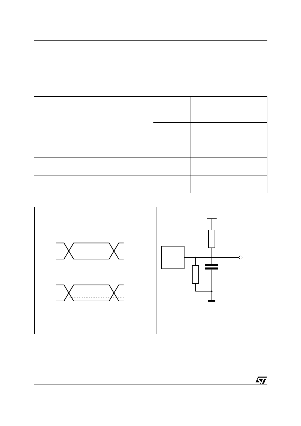
Figure 5. AC Measurement I/O Waveform Figure 6. AC Measurement Load Circuit
V
CC
I/O Timing Reference Voltage
V
CC
0V
Output Transition Timing Reference Voltage
V
CC
0V
VCC/2
0.7V
0.3V
AI04831
DEVICE
UNDER
TEST
R
CC
CC
CL includes probe and 1 TTLcapacitance
R
1
OUT
C
L
2
AI05832
6/18
 Loading...