

SGS Thomson Microelectronics M68AW127B Datasheet
1Mbit (128K x8), 3.0V Asynchronous SRAM
FEATURES SUMMARY
■ SUPPLY VOLTAGE : 2.7 to 3.6V
■ 128K x 8 bits SRAM with OUTPUT ENABLE
■ EQUAL CYCLE and ACCESS TIMES: 70ns
■ LOW STANDBY CURRENT
■ LOW V
■ TRI-STATE COMMON I/O
■ LOW ACTIVE and STAN DBY POWER
DATA RETENTION: 1.5V
CC
M68AW127B
Figure 1. Packages
SO32 (MC)
TSOP32
8 x 20 mm
(N)
TSOP32
8 x 13.4 mm
(NK)
1/20August 2003

M68AW127B
TABLE OF CONTENTS
SUMMARY DESCRIPTION. . . . . . . . . . . . . . . . . . . . . . . . . . . . . . . . . . . . . . . . . . . . . . . . . . . . . . . . . . . 3
Figure 2. Logic Diagram . . . . . . . . . . . . . . . . . . . . . . . . . . . . . . . . . . . . . . . . . . . . . . . . . . . . . . . . . . 3
Figure 5. Block Diagram . . . . . . . . . . . . . . . . . . . . . . . . . . . . . . . . . . . . . . . . . . . . . . . . . . . . . . . . . . 5
Figure 3. SO Connections . . . . . . . . . . . . . . . . . . . . . . . . . . . . . . . . . . . . . . . . . . . . . . . . . . . . . . . . . 4
Figure 4. TSOP Connections . . . . . . . . . . . . . . . . . . . . . . . . . . . . . . . . . . . . . . . . . . . . . . . . . . . . . . . 4
Figure 5. Block Diagram . . . . . . . . . . . . . . . . . . . . . . . . . . . . . . . . . . . . . . . . . . . . . . . . . . . . . . . . . . 5
MAXIMUM RATING. . . . . . . . . . . . . . . . . . . . . . . . . . . . . . . . . . . . . . . . . . . . . . . . . . . . . . . . . . . . . . . . . 5
Table 2. Absolute Maximum Ratings. . . . . . . . . . . . . . . . . . . . . . . . . . . . . . . . . . . . . . . . . . . . . . . . . 5
DC AND AC PARAMETERS. . . . . . . . . . . . . . . . . . . . . . . . . . . . . . . . . . . . . . . . . . . . . . . . . . . . . . . . . . 6
Table 3. Operating and AC Measurement Conditions. . . . . . . . . . . . . . . . . . . . . . . . . . . . . . . . . . . . 6
Figure 6. AC Measurement I/O Waveform . . . . . . . . . . . . . . . . . . . . . . . . . . . . . . . . . . . . . . . . . . . .6
Figure 7. AC Measurement Load Circuit . . . . . . . . . . . . . . . . . . . . . . . . . . . . . . . . . . . . . . . . . . . . . .6
Table 4. Capacitance. . . . . . . . . . . . . . . . . . . . . . . . . . . . . . . . . . . . . . . . . . . . . . . . . . . . . . . . . . . . . 7
Table 5. DC Characteristics. . . . . . . . . . . . . . . . . . . . . . . . . . . . . . . . . . . . . . . . . . . . . . . . . . . . . . . . 7
OPERATION . . . . . . . . . . . . . . . . . . . . . . . . . . . . . . . . . . . . . . . . . . . . . . . . . . . . . . . . . . . . . . . . . . . . . . 8
Table 6. Operating Modes. . . . . . . . . . . . . . . . . . . . . . . . . . . . . . . . . . . . . . . . . . . . . . . . . . . . . . . . .8
Read Mode . . . . . . . . . . . . . . . . . . . . . . . . . . . . . . . . . . . . . . . . . . . . . . . . . . . . . . . . . . . . . . . . . . . . 8
Figure 8. Address Controlled, Read Mode AC Waveforms. . . . . . . . . . . . . . . . . . . . . . . . . . . . . . . . 8
Figure 9. Chip Enable or Output Enable Controlled, Read Mode AC Waveforms. . . . . . . . . . . . . . . 9
Table 7. Read and Standby Mode AC Characteristics . . . . . . . . . . . . . . . . . . . . . . . . . . . . . . . . . . 10
Write Mode . . . . . . . . . . . . . . . . . . . . . . . . . . . . . . . . . . . . . . . . . . . . . . . . . . . . . . . . . . . . . . . . . . . 11
Figure 11. Write Enable Controlled, Write AC Waveforms . . . . . . . . . . . . . . . . . . . . . . . . . . . . . . . 11
Figure 12. Chip Enable Controlled, Write AC Waveforms. . . . . . . . . . . . . . . . . . . . . . . . . . . . . . . . 12
Table 8. Write Mode AC Characteristics . . . . . . . . . . . . . . . . . . . . . . . . . . . . . . . . . . . . . . . . . . . . . 13
Figure 13. E1 Controlled, Low V
Figure 14. E2 Controlled, Low V
Data R e t e n tion A C Wavefo r ms . . . . . . . . . . . . . . . . . . . . . . . . 1 4
CC
Data R e t e n tion A C Wavefo r ms . . . . . . . . . . . . . . . . . . . . . . . . 1 4
CC
Table 9. Low VCC Data Retention Characteristics . . . . . . . . . . . . . . . . . . . . . . . . . . . . . . . . . . . . . 14
PACKAGE MECHANICAL . . . . . . . . . . . . . . . . . . . . . . . . . . . . . . . . . . . . . . . . . . . . . . . . . . . . . . . . . . 15
SO32 - 32 lead Plastic Small Outline, Package Outline . . . . . . . . . . . . . . . . . . . . . . . . . . . . . . . . . 15
SO32 - 32 lead Plastic Small Outline, Package Mechanical Data. . . . . . . . . . . . . . . . . . . . . . . . . . 15
TSO P 3 2 - 32 lea d Plastic Small O u tline 8x 2 0 mm, Package Outl i n e. . . . . . . . . . . . . . . . . . . . . . . . 16
TSOP32 - 32 lead Plastic Small Outline 8x20mm, Packag e Mechani ca l Data . . . . . . . . . . . . . . . . 16
TSOP32 - 32 lead Plastic Small Outline 8x13.4mm, Package Outline . . . . . . . . . . . . . . . . . . . . . . 17
TSOP32 - 32 lead Plastic Small Outline 8x13.4mm, Package M ec hanical Data . . . . . . . . . . . . . . 17
PART NUMBERING . . . . . . . . . . . . . . . . . . . . . . . . . . . . . . . . . . . . . . . . . . . . . . . . . . . . . . . . . . . . . . . 18
Table 13. Ordering Information Scheme . . . . . . . . . . . . . . . . . . . . . . . . . . . . . . . . . . . . . . . . . . . . . 18
REVISION HISTORY. . . . . . . . . . . . . . . . . . . . . . . . . . . . . . . . . . . . . . . . . . . . . . . . . . . . . . . . . . . . . . . 19
Table 14. Document Revision History. . . . . . . . . . . . . . . . . . . . . . . . . . . . . . . . . . . . . . . . . . . . . . .19
2/20
SUMMARY DESCRIPTION
The M68AW127B is a 1Mbit (1,048,576 bit) CMOS
SRAM, organized as 131,072 words by 8 bits. The
device features fully static operat ion requiring no
external clocks or timing strobes, with equal address access and cycle times. It requires a single
2.7 to 3.6V supply.
This device has an automatic power-down feature,
reducing the power consumption by over 99%
when deselected.
The M68AW127B is available in SO32, TSOP 32
8x20mm and TSOP32 8x13.4mm package s.
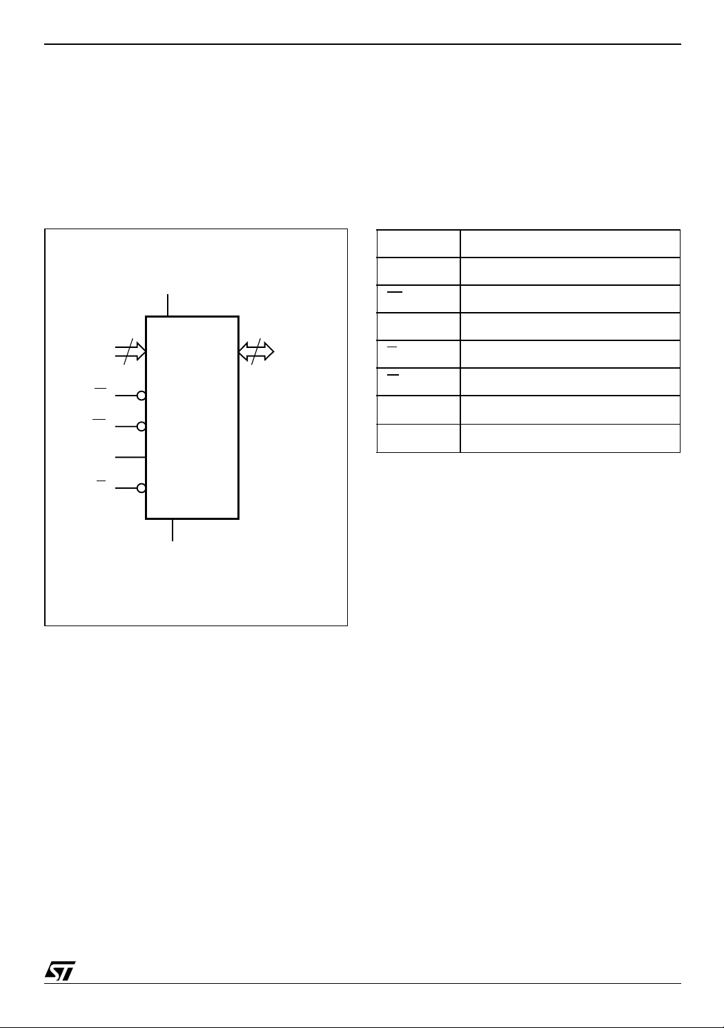
Figure 2. Logic Diagram Table 1. Signal Names
A0-A16 Address Inputs
M68AW127B
A0-A16
W
E1
E2
V
CC
17
M68AW127B
G
V
SS
8
DQ0-DQ7
AI05972b
DQ0-DQ7 Data Input/Output
E1
E2 Chip Enable
G
W
V
CC
V
SS
Chip Enable
Output Enable
Write Enable
Supply Voltage
Ground
3/20
M68AW127B
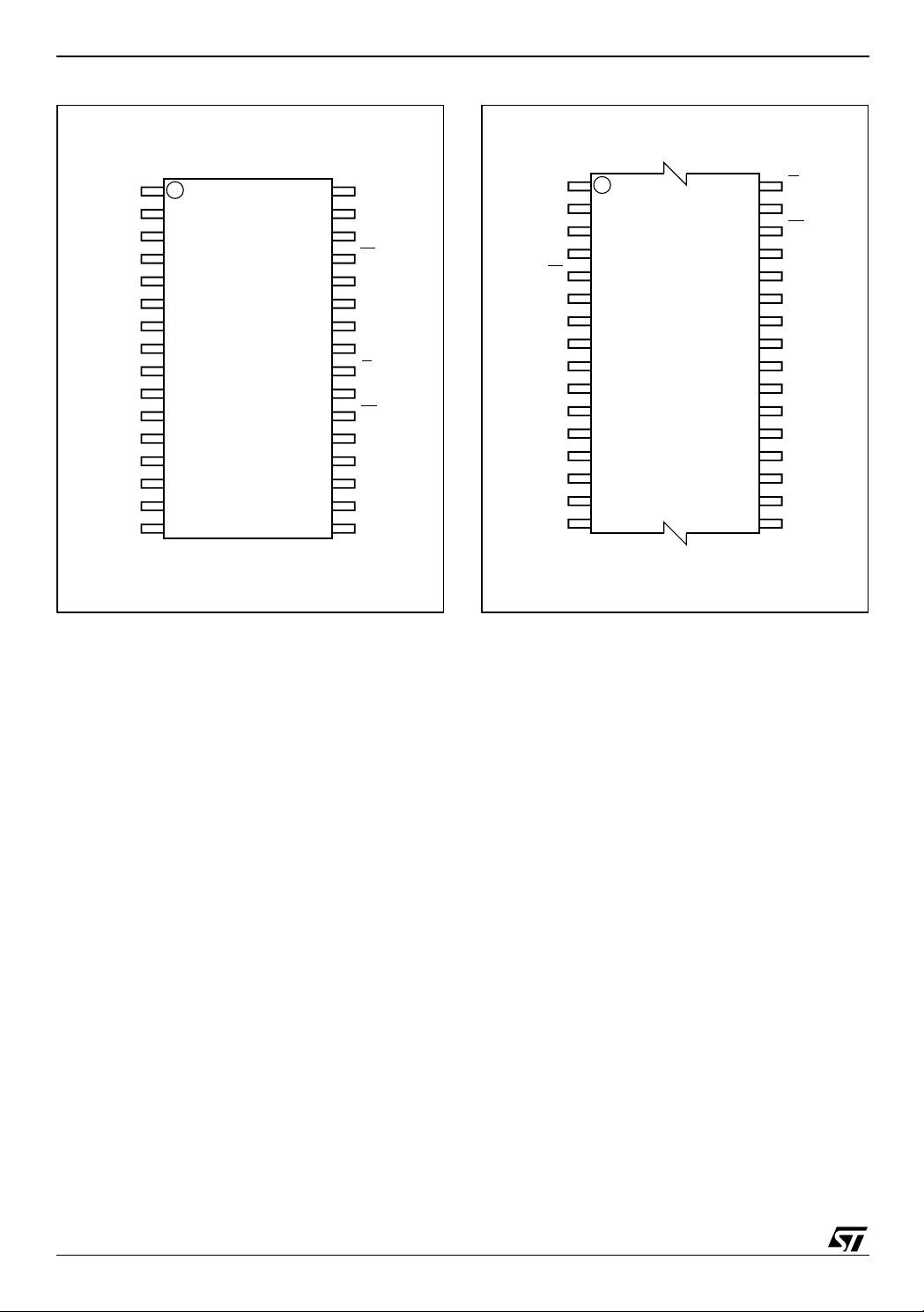
Figure 3. SO Connections Figure 4. TSOP Connections
NC
A16
A14
A12
A7
A6
A5
A4
A3
A2
A1
A0
DQ0
DQ1
DQ2
V
SS
1
8
M68AW127B
9
32
25
24
16 17
AI05931b
V
CC
A15
E2
W
A13
A8
A9
A11
G
A10
E1
DQ7
DQ6
DQ5
DQ4
DQ3
A11
1
32
A9
A8
A13
W
E2
A15
V
CC
NC
8
M68AW127B
9
25
24
A16
A14
A12
A7
A6
A5
A4 A3
16 17
AI05973c
G
A10
E1
DQ7
DQ6
DQ5
DQ4
DQ3
V
SS
DQ2
DQ1
DQ0
A0
A1
A2
4/20
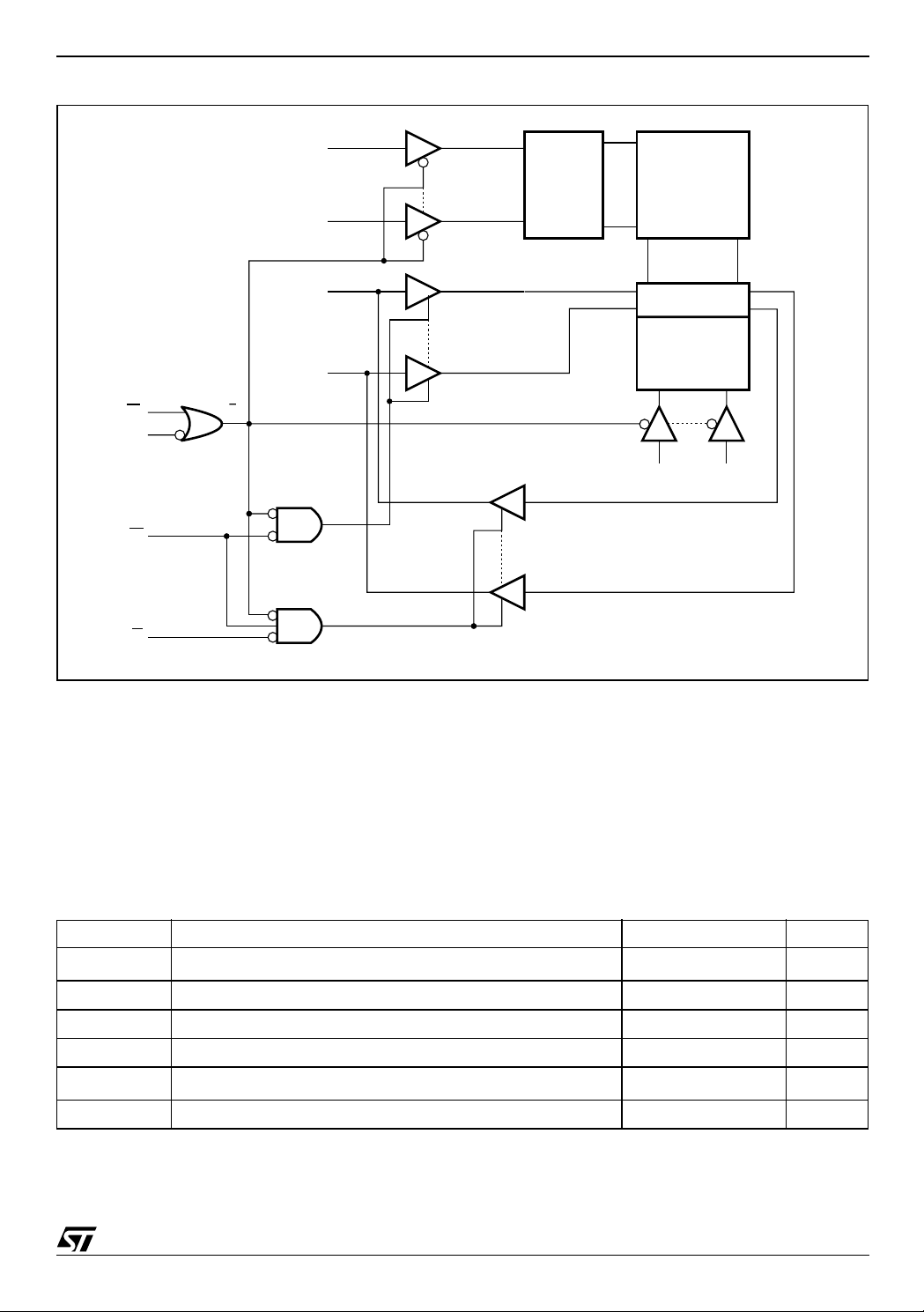
Figure 5. Block Diagram
A16
A7
ROW
DECODER
M68AW127B
MEMORY
ARRAY
DQ7
DQ0
E1
E2
W
G
Ex
MAXIMUM RATIN G
Stressing the device ab ove the rating listed in the
“Absolute Maximum Ratings” table may cause
permanent damage to the device. These are
stress ratings only and operation of the dev ice at
these or any other conditions above those indicated in the Operating sections of this specification is
I/O CIRCUITS
COLUMN
DECODER
A0 A6
AI05471
not implied. Exposure to Absol ute Maxim um Ra ting conditions for extended periods may affect device reliability. Refer also to the
STMicroelectronics SURE Program and other relevant quality documents.
Table 2. Absolute Maximum Ratings
Symbol Parameter Value Unit
(1)
I
O
T
A
T
STG
V
CC
(2)
V
IO
P
D
Note: 1. One output at a time, not to exceed 1 second duration.
2. Up to a maxim um operating V
Output Current 20 mA
Ambient Operating Temperature –55 to 125 °C
Storage Temperature –65 to 150 °C
Supply Voltage –0.3 to 4.6 V
Input or Output Voltage
–0.5 to V
CC
+0.5
Power Dissipation 1 W
of 3.6V only.
CC
V
5/20
M68AW127B
DC AND AC PARAMETERS
This section summarizes the operat ing and measurement conditions, as well as the DC and AC
characteristics of the device. The parameters in
the following DC and AC Characteristic tables are
derived from tests performed under the M easure-
Table 3. Operating and AC Measurement Conditions
Parameter M68AW127B
V
Supply Voltage
CC
Ambient Operating Temperature
ment Conditions listed in the rel evant tables. Designers should check that the operating conditions
in their projects match the measurement conditions when using the quoted parameters.
2.7 to 3.6V
Range 1 0 to 70°C
Range 6 –40 to 85°C
Load Capacitance (C
Output Circuit Protection Resis tance (R
Load Resistance (R
)
L
)
1
)
2
100pF
3.0kΩ
3.1kΩ
Input Rise and Fall Times 1ns/V
Input Pulse Voltages
Input and Output Timing Ref. Voltages
Output Transition Timing Ref. Voltages
V
RL
0 to V
CC
V
/2
CC
= 0.3VCC; VRH = 0.7V
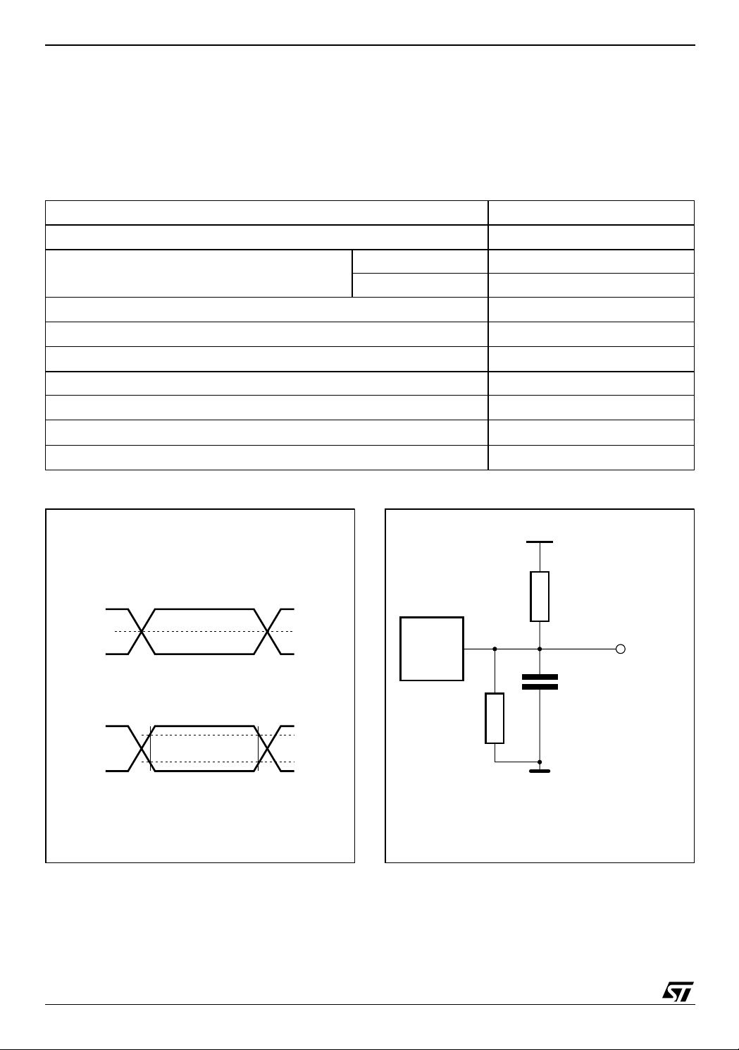
Figure 6. AC Measurement I/O Waveform Figure 7. AC Measurement Load Circuit
V
CC
I/O Timing Reference Voltage
V
CC
0V
Output Transition Timing Reference Voltage
V
CC
0V
VCC/2
0.7V
0.3V
AI04831
DEVICE
UNDER
TEST
R
CC
CC
CL includes JIG capacitance
R
1
OUT
C
L
2
CC
6/20
AI05814
 Loading...