

1 Mbit (64K x16) 3.0V Asynchro nous SRAM
FEATURES SUMMARY
■ SUPPLY VOLTAGE : 2.7 to 3.6V
■ 64K x 16 bits SRAM with OUTPUT ENABLE
■ EQUAL CYCLE and ACCESS TIME: 55ns and
70ns
■ LOW STANDBY CURRENT
■ LOW V
■ TRI-STATE COMMON I/O
■ AUTOMATIC POWER DOWN
DATA RETENTION: 2.0V
CC
M68AW0 64F
Figure 1. Packages
BGA
TFBGA48 (ZB)
6 x 8 solder balls
1/18April 2003

M68AW064F
TABLE OF CONTENTS
SUMMARY DESCRIPTION. . . . . . . . . . . . . . . . . . . . . . . . . . . . . . . . . . . . . . . . . . . . . . . . . . . . . . . . . . . 3
Figure 2. Logic Diagram . . . . . . . . . . . . . . . . . . . . . . . . . . . . . . . . . . . . . . . . . . . . . . . . . . . . . . . . . . 3
Table 1. Signal Names . . . . . . . . . . . . . . . . . . . . . . . . . . . . . . . . . . . . . . . . . . . . . . . . . . . . . . . . . . . 3
Figure 3. TFBGA Connections (Top view through package). . . . . . . . . . . . . . . . . . . . . . . . . . . . . . . 4
Figure 4. Block Diagram . . . . . . . . . . . . . . . . . . . . . . . . . . . . . . . . . . . . . . . . . . . . . . . . . . . . . . . . . . 5
MAXIMUM RATING. . . . . . . . . . . . . . . . . . . . . . . . . . . . . . . . . . . . . . . . . . . . . . . . . . . . . . . . . . . . . . . . . 5
Table 2. Absolute Maximum Ratings. . . . . . . . . . . . . . . . . . . . . . . . . . . . . . . . . . . . . . . . . . . . . . . . . 5
DC AND AC PARAMETERS. . . . . . . . . . . . . . . . . . . . . . . . . . . . . . . . . . . . . . . . . . . . . . . . . . . . . . . . . . 6
Table 3. Operating and AC Measurement Conditions. . . . . . . . . . . . . . . . . . . . . . . . . . . . . . . . . . . . 6
Figure 5. AC Measurement I/O Waveform . . . . . . . . . . . . . . . . . . . . . . . . . . . . . . . . . . . . . . . . . . . . 6
Figure 6. AC Measurement Load Circuit . . . . . . . . . . . . . . . . . . . . . . . . . . . . . . . . . . . . . . . . . . . . . .6
Table 4. Capacitance. . . . . . . . . . . . . . . . . . . . . . . . . . . . . . . . . . . . . . . . . . . . . . . . . . . . . . . . . . . . . 7
Table 5. DC Characteristics. . . . . . . . . . . . . . . . . . . . . . . . . . . . . . . . . . . . . . . . . . . . . . . . . . . . . . . . 7
OPERATION . . . . . . . . . . . . . . . . . . . . . . . . . . . . . . . . . . . . . . . . . . . . . . . . . . . . . . . . . . . . . . . . . . . . . . 8
Table 6. Operating Modes. . . . . . . . . . . . . . . . . . . . . . . . . . . . . . . . . . . . . . . . . . . . . . . . . . . . . . . . . 8
Read Mode . . . . . . . . . . . . . . . . . . . . . . . . . . . . . . . . . . . . . . . . . . . . . . . . . . . . . . . . . . . . . . . . . . . . 8
Figure 7. Address Controlled, Read Mode AC Waveforms. . . . . . . . . . . . . . . . . . . . . . . . . . . . . . . . 8
Figure 8. Chip Enable or Output Enable Controlled, Read Mode AC Waveforms. . . . . . . . . . . . . . . 9
Figure 9. Chip Enable or UB/LB Controlled, Standby Mode AC Waveforms . . . . . . . . . . . . . . . . . . 9
Table 7. Read and Standby Mode AC Characteristics . . . . . . . . . . . . . . . . . . . . . . . . . . . . . . . . . . 10
Write Mode . . . . . . . . . . . . . . . . . . . . . . . . . . . . . . . . . . . . . . . . . . . . . . . . . . . . . . . . . . . . . . . . . . . 11
Figure 10. Write Enable Controlled, Write AC Waveforms . . . . . . . . . . . . . . . . . . . . . . . . . . . . . . . 11
Figure 11. Chip Enable Controlled, Write AC Waveforms. . . . . . . . . . . . . . . . . . . . . . . . . . . . . . . . 12
Table 8. Write Mode AC Characteristics . . . . . . . . . . . . . . . . . . . . . . . . . . . . . . . . . . . . . . . . . . . . . 13
Figure 12. Low V
Table 9. Low V
Data Retention AC Waveforms. . . . . . . . . . . . . . . . . . . . . . . . . . . . . . . . . . . . 14
CC
Data Retention Characteristics. . . . . . . . . . . . . . . . . . . . . . . . . . . . . . . . . . . . . . 14
CC
PACKAGE MECHANICAL . . . . . . . . . . . . . . . . . . . . . . . . . . . . . . . . . . . . . . . . . . . . . . . . . . . . . . . . . . 15
TFBGA48 - 6 x 8 ball array, 0.75 mm pitch, Bottom View Package Outline . . . . . . . . . . . . . . . . . . 15
TFBGA48 - 6 x 8 ball array, 0.75 mm pitch, Package Mechanical Data . . . . . . . . . . . . . . . . . . . . . 15
PART NUMBERING . . . . . . . . . . . . . . . . . . . . . . . . . . . . . . . . . . . . . . . . . . . . . . . . . . . . . . . . . . . . . . . 16
Table 11. Ordering Information Scheme . . . . . . . . . . . . . . . . . . . . . . . . . . . . . . . . . . . . . . . . . . . . . 16
REVISION HISTORY. . . . . . . . . . . . . . . . . . . . . . . . . . . . . . . . . . . . . . . . . . . . . . . . . . . . . . . . . . . . . . . 17
Table 12. Document Revision History. . . . . . . . . . . . . . . . . . . . . . . . . . . . . . . . . . . . . . . . . . . . . . .17
2/18
SUMMARY DESCRIPTION
The M68AW064F is a 1 Mbit (1,048,576 bit)
CMOS SRAM, organized as 65,536 words by 16
bits. The device features fully static opera tion requiring no external clocks or timing strobes, with
equal address access and cycle times. It requires
tomatic power-down feature, redu cing the power
consumption by over 99% when deselected.
The M68AW064F is available in TFBGA48 (0.75
mm pitch) package.
a single 2.7 to 3.6V supply. This device has an au-
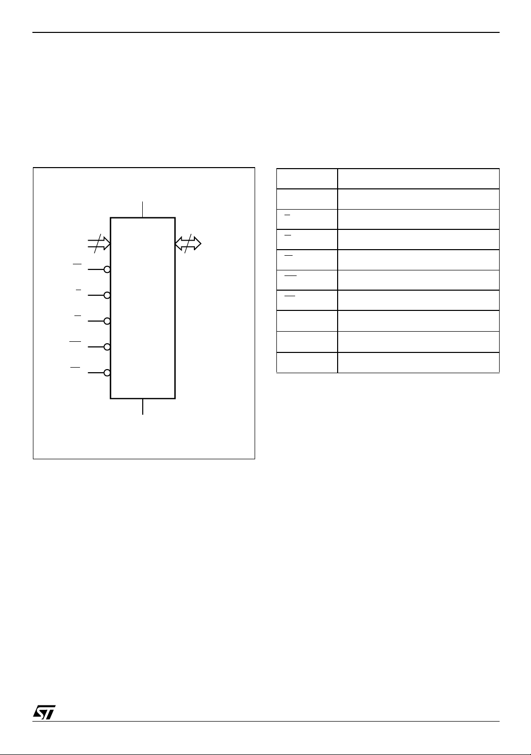
Figure 2. Logic Diagram Table 1. Signal Names
A0-A15 Address Inputs
V
CC
DQ0-DQ15 Data Input/Output
M68AW064F
A0-A15
W
UB
LB
16
16
DQ0-DQ15
E
M68AW064F
G
V
SS
AI04872b
E
G
W
UB
LB
V
CC
V
SS
NC Not Connected Internally
Chip Enable
Output Enable
Write Enable
Upper Byte Enable Input
Lower Byte Enable Input
Supply Voltage
Ground
3/18
M68AW064F
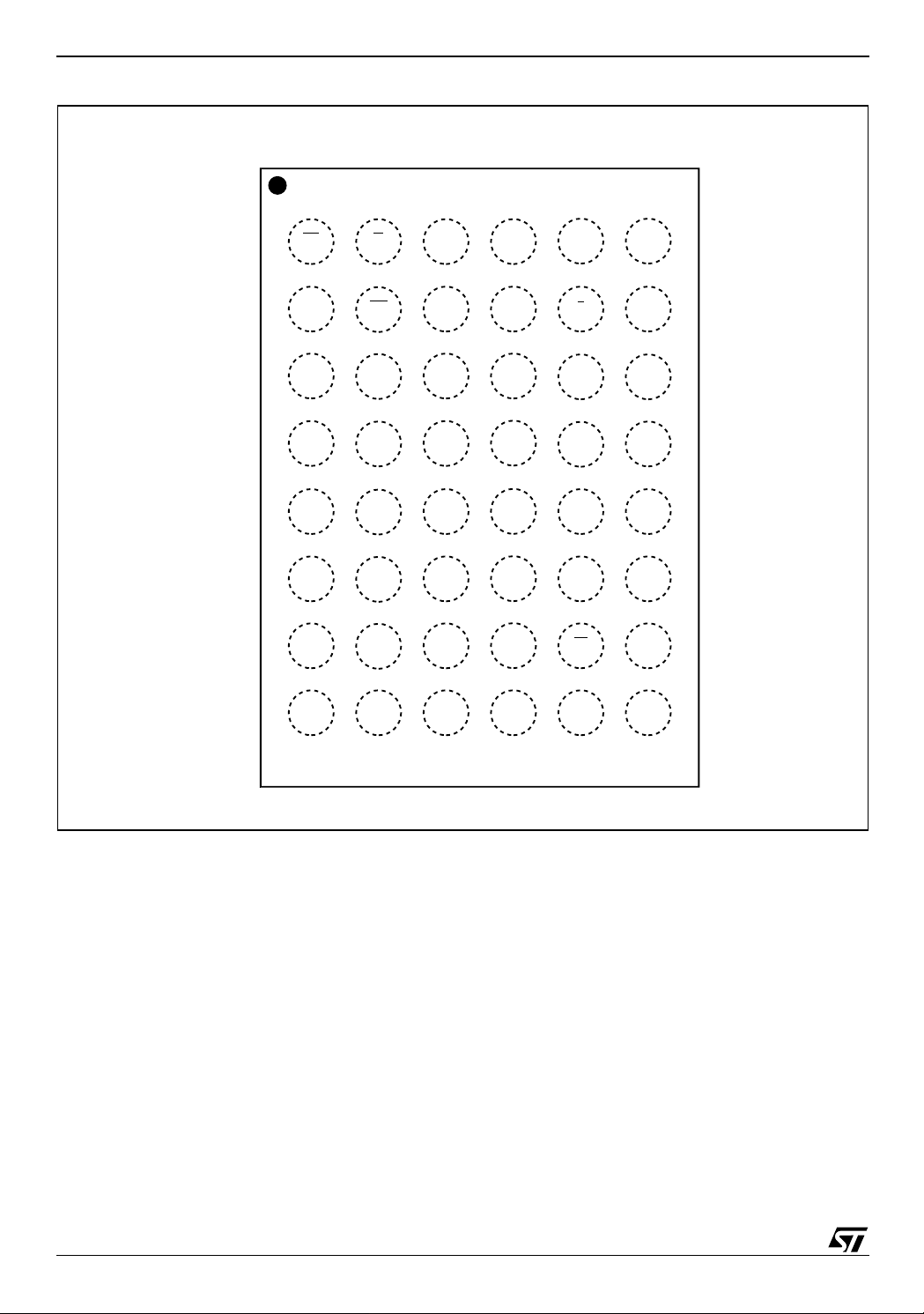
Figure 3. TFBGA Connections (Top view through package)
654321
A
B
C
D
E
F
G
H
DQ8
DQ9
V
SS
V
CC
DQ14
DQ15
UB
DQ10
DQ11
DQ12
DQ13
NC
A0GLB
NC
NC V
A14
A9
A1
A4 E
A6A5
A7
NC
A15
A13
A10
A2 NC
DQ3
DQ4
DQ5
DQ0A3
DQ2DQ1
V
CC
SS
DQ6
DQ7WA12
NCA11A8NC
4/18
AI04874
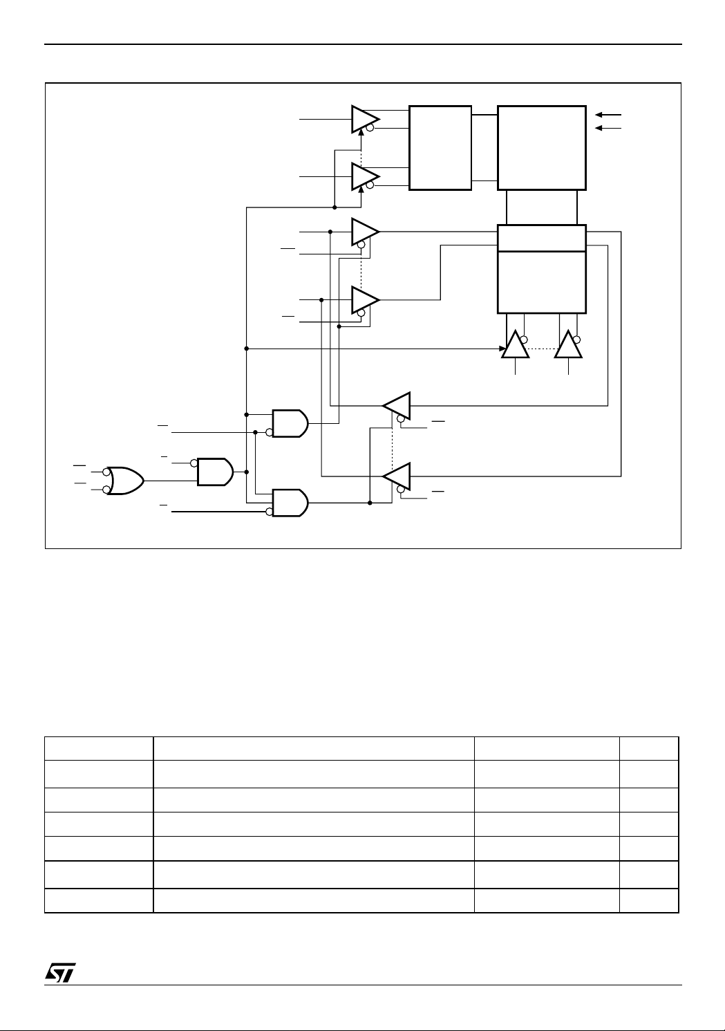
Figure 4. Block Diagram
A15
A7
ROW
DECODER
MEMORY
ARRAY
M68AW064F
V
CC
V
SS
DQ15
UB
DQ0
LBLB
W
UB
LB
E
G
MAXIMUM RATI NG
Stressing the device ab ove the rating listed in t he
Absolute Maximum Ratings" table may cause permanent damage to the device. These are stress
ratings only and operation of the device at these or
any other conditions ab ove those i ndicated in t he
Operating sections of this specificat ion is not im-
(8)
(8)
(8)
UB
(8)
LB
I/O CIRCUITS
COLUMN
DECODER
A0 A6
AI04875
plied. Exposure to Absolute Maximum Rating conditions for extended periods may affect device
reliability. Refer also to the STMicroelectronics
SURE Program and ot her relevant quality documents.
Table 2. Absolute Maximum Ratings
Symbol Parameter Value Unit
(1)
I
O
T
A
T
STG
V
CC
(2)
V
IO
P
D
Note: 1. One out put at a time, not to exceed 1 second durat i on.
2. Up to a maxim um operating V
Output Current 20 mA
Ambient Operating Temperature –55 to 125 °C
Storage Temperature –65 to 150 °C
Supply Voltage –0.5 to 4.6 V
Input or Output Voltage
–0.5 to V
CC
+0.5
Power Dissipation 1 W
of 3.6V only.
CC
V
5/18
M68AW064F
DC AND AC PARAMETERS
This section summarizes the operat ing and measurement conditions, as well as the DC and AC
characteristics of the device. The parameters in
the following DC and AC Characteristic tables are
derived from tests performed under the M easure-
Table 3. Operating and AC Measurement Conditions
Parameter M68AW064F
Supply Voltage
V
CC
Ambient Operating Temperature –40 to 85°C
Load Capacitance (C
Output Circuit Protection Resis tance (R
Load Resistance (R
Input Rise and Fall Times
Input Pulse Voltages
Input and Output Timing Ref. Voltages
Input and Output Transition Timing Ref. Voltages
)
L
)
1
)
2
ment Conditions listed in the rel evant tables. Designers should check that the operating conditions
in their projects match the measurement conditions when using the quoted parameters.
2.7 to 3.6V
30 or 5pF
1.10k
1.55k
4ns
≤
0 to V
V
CC
V
= 0.3VCC; VOH = 0.7V
OL
Ω
Ω
CC
/2
CC
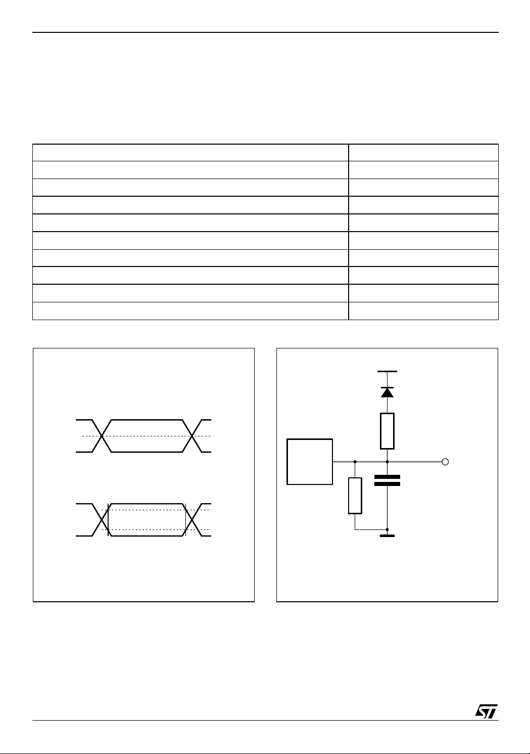
Figure 5. AC Measurement I/O Waveform Figure 6. AC Measurement Load Circuit
V
CC
I/O Timing Reference Voltage
V
CC
0V
I/O Transition Timing Reference Voltage
V
CC
0V
VCC/2
0.7V
0.3V
AI04831
CC
CC
DEVICE
UNDER
TEST
R
2
CL includes JIG capacitance
1N914
R
1
OUT
C
L
AI03853
6/18
 Loading...