

16 Mbit (1M x16) 1.8V Asynchronous SRAM
FEATURES SUMMARY
■ SUPPLY VOLTAGE: 1.65 to 1.95V
■ I/O SUPPLY VOLTAGE: 1.5 to 1.95V
■ 1M WORDS x 16 bits LOW POWER SRAM
■ EQUAL CYCLE and ACCESS TIME: 70ns
■ LOW V
■ LOW STANDBY CURRENT
■ TRI-STATE COMMON I/O
■ SINGLE BYTE READ/W R ITE
■ AUTOMATIC POWER DOWN
DATA RETENTION: 1.0V
CC
M68AR024D
PRELIMINARY DATA
Figure 1. Packages
BGA
TFBGA48 (ZH)
8 x 10 mm
(for Engineering
Samples only)
BGA
TFBGA48 (ZB)
6.5 x 10 mm
October 2002
This is preliminary information on a new product now in development or undergoing evaluation. Details are subject to change without notice.
1/19

M68AR024D
TABLE OF CONTENTS
SUMMARY DESCRIPTION. . . . . . . . . . . . . . . . . . . . . . . . . . . . . . . . . . . . . . . . . . . . . . . . . . . . . . . . . . . 3
Figure 2. Logic Diagram . . . . . . . . . . . . . . . . . . . . . . . . . . . . . . . . . . . . . . . . . . . . . . . . . . . . . . . . . . 3
Table 1. Signal Names . . . . . . . . . . . . . . . . . . . . . . . . . . . . . . . . . . . . . . . . . . . . . . . . . . . . . . . . . . . 3
Figure 3. TFBGA Connections (Top view through package). . . . . . . . . . . . . . . . . . . . . . . . . . . . . . . 4
Figure 4. Block Diagr am . . . . . . . . . . . . . . . . . . . . . . . . . . . . . . . . . . . . . . . . . . . . . . . . . . . . . . . . . . 5
MAXIMUM RATING. . . . . . . . . . . . . . . . . . . . . . . . . . . . . . . . . . . . . . . . . . . . . . . . . . . . . . . . . . . . . . . . . 5
Table 2. Absolute Maximum Ratings. . . . . . . . . . . . . . . . . . . . . . . . . . . . . . . . . . . . . . . . . . . . . . . . . 5
DC AND AC PARAMETERS. . . . . . . . . . . . . . . . . . . . . . . . . . . . . . . . . . . . . . . . . . . . . . . . . . . . . . . . . . 6
Table 3. Operating and AC Measurement Conditions. . . . . . . . . . . . . . . . . . . . . . . . . . . . . . . . . . . . 6
Figure 5. AC Measurement I/O Waveform . . . . . . . . . . . . . . . . . . . . . . . . . . . . . . . . . . . . . . . . . . . . 6
Figure 6. AC Measurement Load Circuit . . . . . . . . . . . . . . . . . . . . . . . . . . . . . . . . . . . . . . . . . . . . . .6
Table 4. Capacitance. . . . . . . . . . . . . . . . . . . . . . . . . . . . . . . . . . . . . . . . . . . . . . . . . . . . . . . . . . . . . 7
Table 5. DC Character i stics. . . . . . . . . . . . . . . . . . . . . . . . . . . . . . . . . . . . . . . . . . . . . . . . . . . . . . . . 7
OPERATION . . . . . . . . . . . . . . . . . . . . . . . . . . . . . . . . . . . . . . . . . . . . . . . . . . . . . . . . . . . . . . . . . . . . . . 8
Table 6. Operating Modes. . . . . . . . . . . . . . . . . . . . . . . . . . . . . . . . . . . . . . . . . . . . . . . . . . . . . . . . . 8
Read Mode . . . . . . . . . . . . . . . . . . . . . . . . . . . . . . . . . . . . . . . . . . . . . . . . . . . . . . . . . . . . . . . . . . . . 8
Figure 7. Address Controlled, Read Mode AC Waveforms. . . . . . . . . . . . . . . . . . . . . . . . . . . . . . . . 8
Figure 8. Chip Enable or Output Enable Controlled, Read Mode AC Waveforms . . . . . . . . . . . . . . 9
Figure 9. Chip Enable or UB/LB Controlled, Standby Mode AC Waveforms . . . . . . . . . . . . . . . . . . 9
Table 7. Read and Standby Mode AC Characteristics . . . . . . . . . . . . . . . . . . . . . . . . . . . . . . . . . . 10
Write Mode . . . . . . . . . . . . . . . . . . . . . . . . . . . . . . . . . . . . . . . . . . . . . . . . . . . . . . . . . . . . . . . . . . . 11
Figure 10. Write En a ble Controlled, Writ e AC Waveforms . . . . . . . . . . . . . . . . . . . . . . . . . . . . . . . 11
Figure 11. Chip Enable E1 Controlled, Write AC Waveforms . . . . . . . . . . . . . . . . . . . . . . . . . . . . . 12
Figure 12. UB/LB Controlled, Write AC Waveforms . . . . . . . . . . . . . . . . . . . . . . . . . . . . . . . . . . . . 12
Table 8. Write Mode AC Characteristics . . . . . . . . . . . . . . . . . . . . . . . . . . . . . . . . . . . . . . . . . . . . . 13
Figu r e 1 3 . E1 Con troll e d , L o w VCC D a ta Reten tion A C Wave fo rms . . . . . . . . . . . . . . . . . . . . . . . 1 4
Figu r e 1 4 . E2 Cont r o l led, Lo w VCC Data Re tenti o n AC Waveforms . . . . . . . . . . . . . . . . . . . . . . . 14
Table 9. Low VCC Data Retention Characteristics . . . . . . . . . . . . . . . . . . . . . . . . . . . . . . . . . . . . . 14
PACKAGE MECHANICAL . . . . . . . . . . . . . . . . . . . . . . . . . . . . . . . . . . . . . . . . . . . . . . . . . . . . . . . . . . 15
Figure 15. TFBGA48 6.5x10mm - 6x8 ball array, 0.75 mm pitch, Bottom View Package Outline. . 15
Table 11. TFBGA48 8x10mm - 6x8 ball array, 0.75 mm pitch, Package Mechanical Data. . . . . . . 16
PART NUMBERING . . . . . . . . . . . . . . . . . . . . . . . . . . . . . . . . . . . . . . . . . . . . . . . . . . . . . . . . . . . . . . . 17
Table 12. Ordering Information Scheme . . . . . . . . . . . . . . . . . . . . . . . . . . . . . . . . . . . . . . . . . . . . .17
REVISION HISTORY. . . . . . . . . . . . . . . . . . . . . . . . . . . . . . . . . . . . . . . . . . . . . . . . . . . . . . . . . . . . . . . 18
Table 13. Document Revision History. . . . . . . . . . . . . . . . . . . . . . . . . . . . . . . . . . . . . . . . . . . . . . .18
2/19
SUMMARY DESCRIPTION
The M68AR024D is a 16 Mbit (16, 777,216 bit) Low
Power SRAM fabricated in STMicroelectronics advanced CMOS technology, organiz ed as 1,048,576
words by 16 bit s. The device exhi bits f ully sta tic op eration requiring no external clocks or timing
strobes.
It needs 1.65 to 1.95V supply voltage. By using the
pin all the outputs can be powered indepen-
V
CCQ
dently from the core supply voltage allowing to
drive the I/O pins down to 1.5V. V
pin can be
CCQ
tied to Vcc if the feature is not required.
This device has a standard Asynchronous SRAM
Interface. Read and Write cycles can be performed on a single byte by using UB
The device can be put into standby mode by using
/E2 pins. The same pins can be used to cas-
E1
cade more devices in order to achieve deep memory expansion.
Standby mode allows a low current consu mption,
up to 99%, by reducing internal activities.
The M68AR024D is available in TFBGA48 (0.75
mm pitch) package with industrial standard footprint.
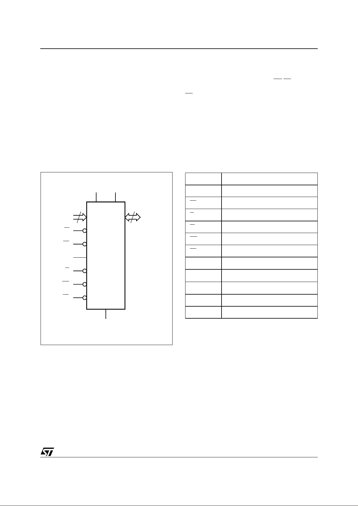
Figure 2. Logic Diagram Table 1. Signal Names
A0-A19 Address Inputs
V
V
CC
A0-A19
W
E1
E2
UB
LB
CCQ
20
M68AR024D
G
16
DQ0-DQ15
DQ0-DQ15 Data Input/Output
, E2 Chip Enables
E1
G
W
UB
LB
V
CC
V
CCQ
V
SS
NC Not Connected Internally
Output Enable
Write Enable
Upper Byte Enable Input
Lower Byte Enable Input
Supply Voltage
I/O Supply Voltage
Ground
M68AR024D
/LB signals.
DU Don’t Use as Internally Connected
V
SS
AI05400c
3/19
M68AR024D
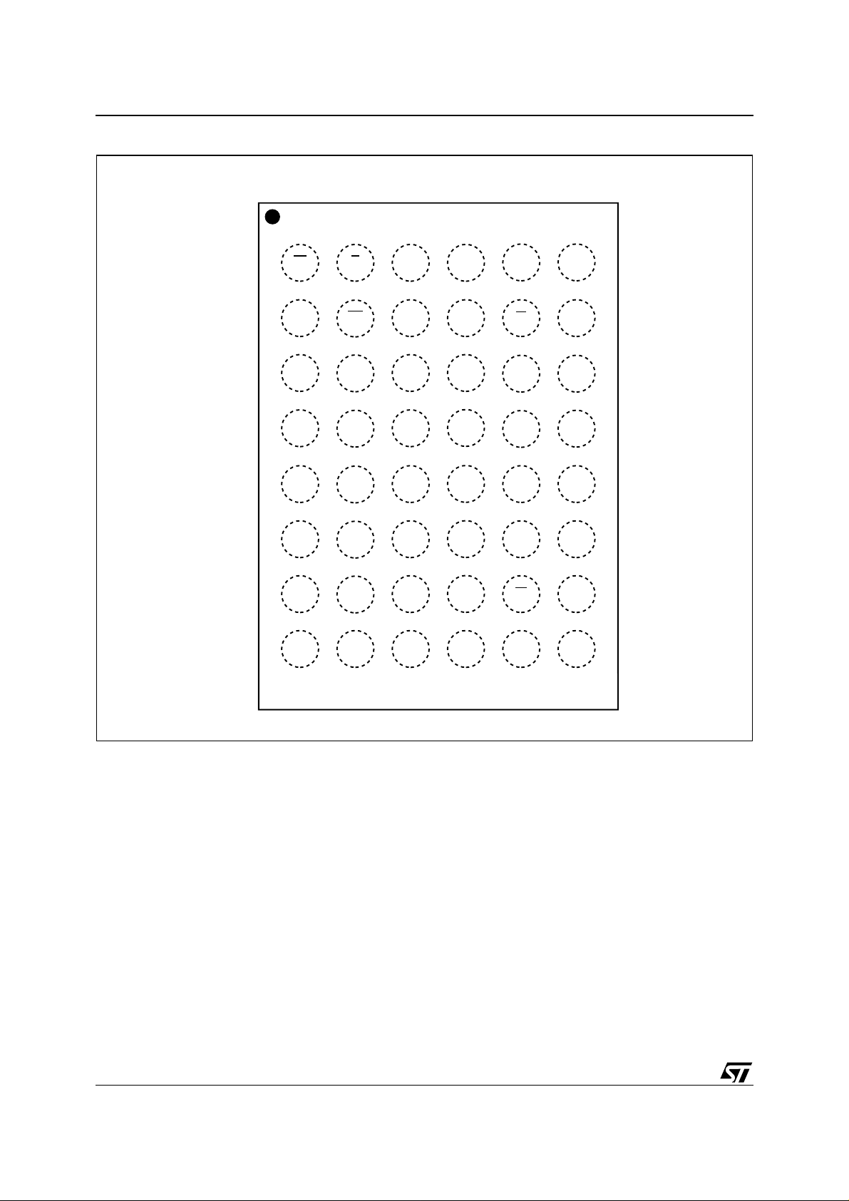
Figure 3. TFBGA Connections (Top view through package)
654321
A
B
C
D
E
F
G
H
LB
DQ8
DQ9
V
SS
V
CCQ
DQ14
DQ15
UB
DQ10
DQ11
DQ12
DQ13
A19
A0G
A17
NC V
A14
A9
A1
A4 E1
A6A5
A7
A16
A15
A13
A10
A2 E2
DQ3
DQ4
DQ5
DQ0A3
DQ2DQ1
V
CC
SS
DQ6
DQ7WA12
DUA11A8A18
4/19
AI05918
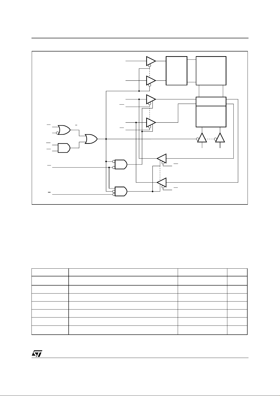
Figure 4. Block Diagram
A19
A8
ROW
DECODER
M68AR024D
MEMORY
ARRAY
DQ15
UB
E1
E2
UB
LB
Ex
W
G
DQ0
LBLB
MAXIMUM RATIN G
Stressing the device above the rating l isted in the
Absolute Maximum Ratings table m ay cause permanent damage to the device. These are stress
ratings only and operation of the device at t hese or
any other conditions ab ove those i ndicated in t he
Operating sections of this specificat ion is not im-
(8)
(8)
(8)
UB
(8)
LB
I/O CIRCUITS
COLUMN
DECODER
A0 A7
AI05924
plied. Exposure to Absolute Maximum Rating conditions for periods greater than 1 sec may affect
device reliability. Refer also to the STMicroelectronics SURE Program and other relevant quality
documents.
Table 2. Absolute Maximum Ratings
Symbol Parameter Value Unit
(1)
I
O
P
D
T
A
T
STG
V
CC
V
CCQ
(2)
V
IO
Note: 1. One output at time not to exceed 1 secon d duration.
2. Up to a m aximum operating V
Output Current 20 mA
Power Dissipation 1 W
Ambient Operating Temperature –55 to 125 °C
Storage Temperature –65 to 150 °C
Supply Voltage –0.5 to 2.5 V
I/O Supply Voltage –0.5 to 2.5 V
Input or Output Voltage
or V
CC
CCQ
–0.5 to V
of 1.95V on l y.
CCQ
+0.5
V
5/19
M68AR024D
DC AND AC PARAMETERS
This section summarizes the operat ing and measurement conditions, as well as the DC and AC
characteristics of the device. The parameters in
the following DC and AC Characteristic tables are
derived from tests performed under the M easure-
Table 3. Operating and AC Measurement Conditions
Parameter M68AR02 4D
Supply Voltage
V
CC
I/O Supply Voltage (V
V
CCQ
Ambient Operating Temperature
CCQ
V
≤
)
CC
ment Conditions listed i n the relevant tables. Designers should check that the operating conditions
in their projects match the measurement conditions when using the quoted parameters.
1.65 to 1.95V
1.5 to 1.95V
Range 1 0 to 70°C
Range 6 –40 to 85°C
Load Capacitance (C
Output Circuit Protection Resis tance (R
Load Resistance (R
Input Rise and Fall Times
Input Pulse Voltages
Input and Output Timing Ref. Voltages
Output Transition Timing Ref. Voltages
)
L
)
1
)
2
= 0.3V
V
RL
30pF
15.3k
11.3k
1ns/V
≤
0 to V
CCQ
V
CCQ
; VRH = 0.7V
CCQ
Ω
Ω
/2
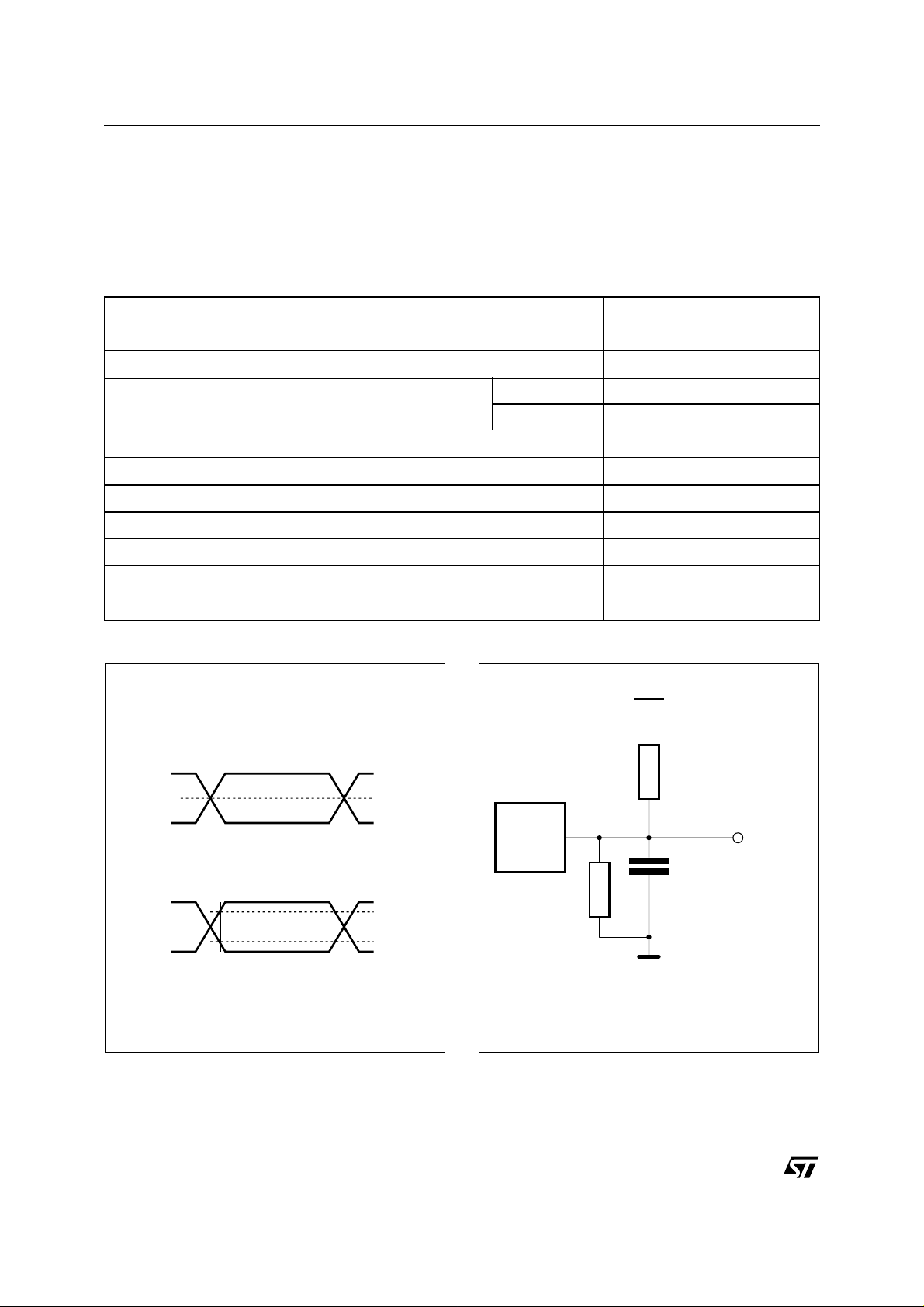
Figure 5. AC Measurement I/O Waveform Figure 6. AC Measurement Load Circuit
V
CCQ
I/O Timing Reference Voltage
R
V
CCQ
0V
I/O Transition Timing Reference Voltage
V
CCQ
0V
V
CCQ
0.7V
0.3V
AI05987
/2
CCQ
CCQ
DEVICE
UNDER
TEST
R
2
CL includes JIG capacitance
1
OUT
C
L
CCQ
6/19
AI05988
 Loading...