

128 Kbit (8 Kbit x 16) SRAM WITH OUTPUT ENABLE
FEATURES SUMMARY
■ OPERATION VOLTAGE: 2.34V to 3.6V
■ 8 Kbit x 16 SRAM
■ EQUAL CYCLE and ACCESS TIMES: AS
FAST AS 20ns
■ TRI-STATE COMMON I/O
■ TWO WRITEENABLE PINSALLOWWRITING
TO UPPER AND LOWER BYTES
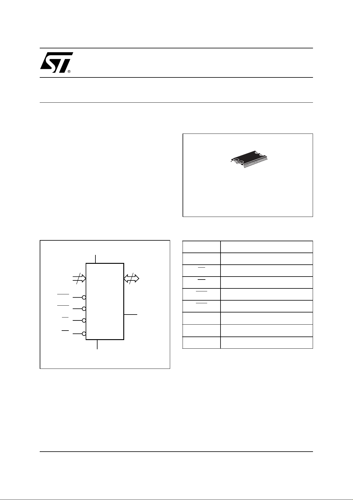
Figure 2. Logic Diagram Table 1. Signal Names
Figure 1. 44-pin, Hatless SOIC Package
44
SO44 (MH)
M616Z08
1
A0-A12
WE0
WE1
CE
OE
13
V
CC
M616Z08
V
SS
16
DQ0-DQ15
TO
AI04213
A0-A12 Address Inputs
DQ0-DQ15 Data Input/Output
CE
OE
WE0
WE1
V
CC
V
SS
TO Time-Out Pin
Note: TO Pin should be connected to VCC.
Chip Enable
Output Enable
WRITE Enable DQ 0-7
WRITE Enable DQ 8-15
Supply Voltage
Ground
1/14July 2002

M616Z08
TABLE OF CONTENTS
DESCRIPTION ....................................................................3
44-pin Connec t ions (Figure 3.) . . . ..................................................3
MAXIMUMRATING.................................................................4
AbsoluteMaximumRatings(Table2.) ...............................................4
DC AND AC PARAM ETERS. . ........................................................5
DC and AC Measurement Conditions (Table 3.). . . .....................................5
AC Test ing Load Circuit (Figure 4.)..................................................5
Capacitance (Table 4.) . . . ........................................................5
DCCharacteristics(Table5.)......................................................6
OPERATION......................................................................6
READMode....................................................................6
AddressControlled,READModeACWaveforms(Figure5.)..............................6
Chip Enable or Output Enable Controlled, READ Mode AC Waveforms (Figure 6.). . ...........7
READModeACCharacteristics(Table6.)............................................7
WRITEMode...................................................................8
WRITE Enable Controlled, WRITE Mode AC W av eforms ( Figure 7.)........................8
ChipEnableControlled,WRITEModeACWaveforms(Figure8.)..........................8
WRITEModeACCharacteristics(Table7.)...........................................9
“Operational” Mode .............................................................10
NoiseImmunity................................................................10
WE(0,1)StatesduringAccess(Table8.)............................................10
Operating Modes (Table 9.).......................................................10
PARTNUMBERING...............................................................11
PACKAGE MECHANICAL INFORMATION . . . ..........................................12
REVISIONHISTORY...............................................................13
2/14
DESCRIPTION
The M616Z08 is a 128 Kbit (131,072 bit) CMOS
SRAM, organized by 16 bits. The device features
fullystatic operation requiring noexterna l clocks or
timing strobes, with equal address access and cycle times. It requires a single 2.6V ± 10% or
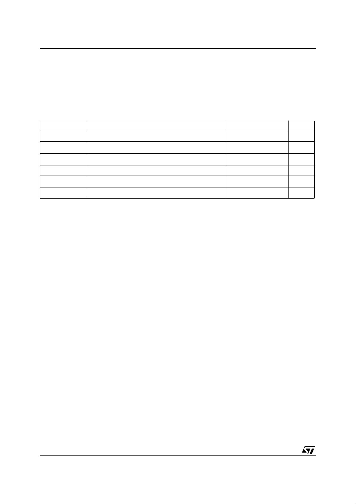
Figure 3. 44-pin Connections
M616Z08
3.3V ± 10% supply, and all inputs and outputs are
TTL compat ible.
The M616Z08 is available in a 44-lead SOIC package.
DQ0
DQ1
DQ2
DQ3
V
CC
V
SS
DQ4
DQ5
DQ6
DQ7
V
CC
V
SS
DQ8
DQ9
DQ10
DQ11
V
SS
V
CC
DQ12
DQ13
DQ14
DQ15
1
2
3
4
5
6
7
8
9
10
11
12
13
14
15
16
17
18
19
20
21
22
M616Z08
44
43
42
41
40
39
38
37
36
35
34
33
32
31
30
29
28
27
26
25
24
23
A12
A11
A10
A9
V
CC
V
SS
A08
A07
TO
CE
OE
WE1
WE0
A06
A05
A04
V
SS
V
CC
A03
A02
A01
A00
AI04212
Note: TO Pin should be connected to VCC.
3/14
M616Z08
MAXIMUM RATING
Stressingthedeviceabovetheratinglistedinthe
“Absolute Maximum Ratings” table may caus e
permanent damage to the device. These are
stress ratings only and operation of the device at
these or any other conditions above those indicated in the Ope ra ting sections of this specification is
Table 2. Absolute Maximum Ratings
Symbol Parameter Value Unit
T
A
(1)
T
STG
(2,3)
V
IO
V
CC
(4)
I
O
P
D
Note: 1. Reflow at peak temperature of 215°C to 225°C for < 60 seconds (total thermal budget not to exceed 180°C for between 90 and 120
seconds).
2. Upto a maximum operating V
(min)= VSS–2.0VAC(pulsewidth≤10% t
3. V
IL
V
(max)= VCC+ 2.0V AC (pulse width ≤ 10% t
IH
4. Oneoutput at a time, not to exceed 1 second duration.
Ambient Operating Temperature –40 to 125 °C
Storage Temperature –65 to 150 °C
Input or Output Voltage
Supply Voltage –0.3 to 4.0 V
Output Current 10 mA
Power Dissipation 270 mW
of 3.6V only.
CC
AVAV
AVAV
(min))
(min))
not implied. Exposure to Absolute Maximum Rating conditions for extended periods may affec t device reliability. Refer also to the
STMicroelectronics SURE Program and other relevant quality documents.
–0.3 to V
CC
+ 0.3
V
4/14
DC AND AC PARAM ETERS
This section summarizes the operating and measurement conditions, as well as the DC and AC
characteristics of the device. The parameters in
the following DC and AC Characteristic tables are
ment Conditions listed in the relevant tables. Designers should check that the operating conditions
in their projects match the measure ment conditions when using the quoted parameters.
derived from tests performed under the Measure-
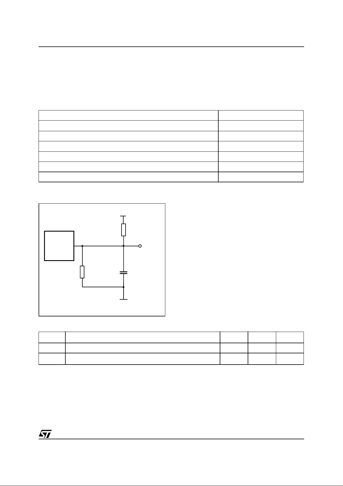
Table 3. DC and AC Measurement Conditions
Parameter M616Z08
Supply Voltage
V
CC
Ambient Operating Temperature –40 to 125°C
2.34 to 3.0V or 3.0 to 3.6V
M616Z08
Load Capacitance (C
Input Rise and Fall Times ≤ 5ns
Input Pulse Voltages 0to3V
Input and Output Timing Ref. Voltages 1.5V
Note: Output High Z is defined as the point where data is no longer driven.
)
L
50pF
Figure 4. AC Testing Load Circuit
3.0V
2.6 KΩ
DEVICE
UNDER
TEST
2.6 KΩ
OUT
CL = 50 pF
or 5pF
AI05650
Table 4. Capacitance
Symbol
C
C
OUT
Note: 1. Effective capacitance measured with power supply at 3.3V; sampled only, not 100% tested.
Input Capacitance on all pins (except DQ) 10 pF
IN
(3)
Output Capacitance 10 pF
2. A t 25°C; f = 1MHz.
3. Outputs deselected.
Parameter
(1,2)
Min Max Unit
5/14
 Loading...