

32 Mbit (2Mb x16, Mux I/O, Dual Bank, Burst)
■ SUPPLY VOLTAGE
= V
–V
DD
Erase and Read
–V
= 12V for fast Program (optional)
PP
■ MULTIPLEXED ADDRESS/DATA
■ SYNCHRONOUS / ASYNCHRONOUS READ
– Configurable Burst mode Read
– Page mode Read (4 Words Page)
– Random Access: 100ns
■ PROGRAMMING TIME
– 10µs by Word typical
– Double Word Programming Option
■ MEMORY BLOCKS
– Dual Ba nk Memory Ar ray: 8 Mb i t - 24 Mbi t
– Parameter Blocks (Top or Bottom location)
■ DUAL BANK OPERATIONS
– Read within one Bank while Program or
Erase within the other
– No delay between Read and Write operations
■ BLOCK PROTECTION/UNPROTECTION
– All Blocks protected at Power-up
– Any combination of Blocks can be protected
■ COMMON FLASH INTERFACE (CFI)
■ 64 bit SECURITY CODE
■ ERASE SUSPEND and RESUME MODES
■ 100,000 PROGRAM/ER ASE CYCL ES per
BLOCK
■ ELECTRONIC SIGNATURE
– Manufacturer Code: 20h
– Top Device Code, M59MR032C: A4h
– Bottom Device Code, M59MR032D: A5h
= 1.65V to 2.0V for Program,
DDQ
M59MR032C
M59MR032D
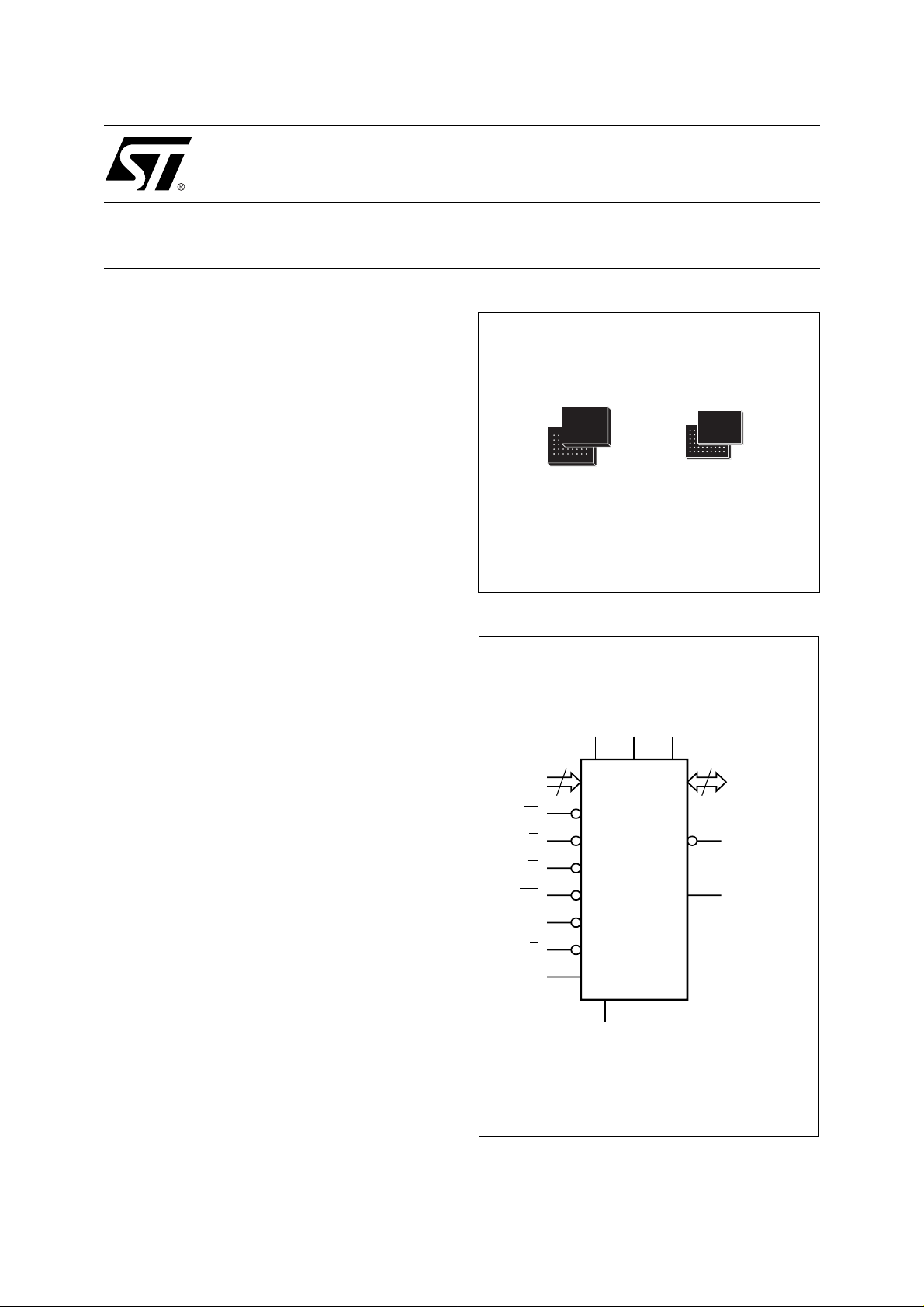
1.8V Supply Flash Memory
BGA
LFBGA54 (ZC)
10 x 4 ball array
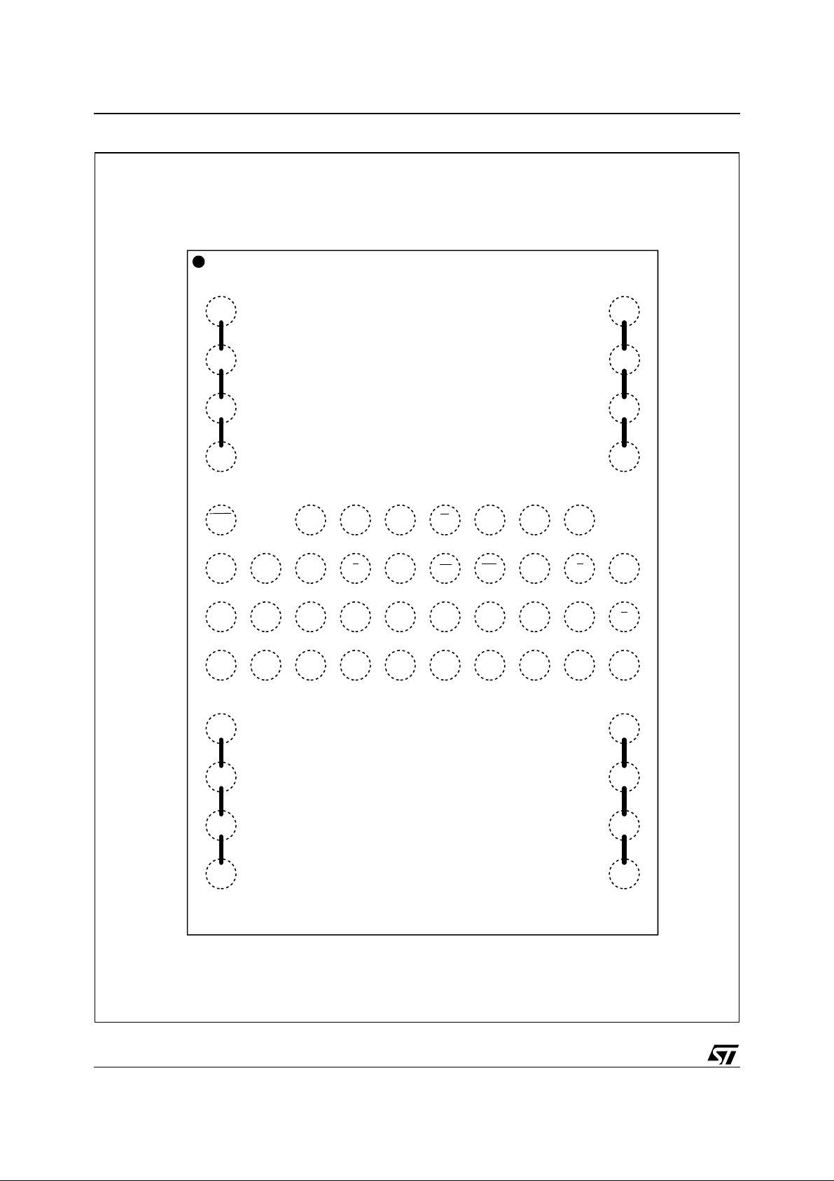
Figure 1. Logic Diagram
V
V
DDQVPP
DD
5
A16-A20
W
E
G
RP
WP
L
K
M59MR032C
M59MR032D
V
SS
µBGA
µBGA46 (GC)
10 x 4 ball array
16
ADQ0-ADQ15
WAIT
BINV
AI90109
1/49April 2001
M59MR032C, M59MR032D
Figure 2. LFBGA Connections (Top view through package)
87654321
A
B
C
D
F
G
DU
DU
DU
DU
DDQ
SS
V
SS
KWAITE
ADQ13 ADQ12
DD
V
WV
WPRPBINVLA20A16V
ADQ2ADQ3ADQ6ADQ7V
PP
A19
A18
ADQ9
A17
E
ADQ8
109
DU
DU
DU
DU
V
SS
G
2/49
ADQ14ADQ15H
J
K
L
M
DU
DU
DU
DU
SS
ADQ10ADQ11ADQ4ADQ5V
V
DDQ
ADQ1
ADQ0
DU
DU
DU
DU
AI90110
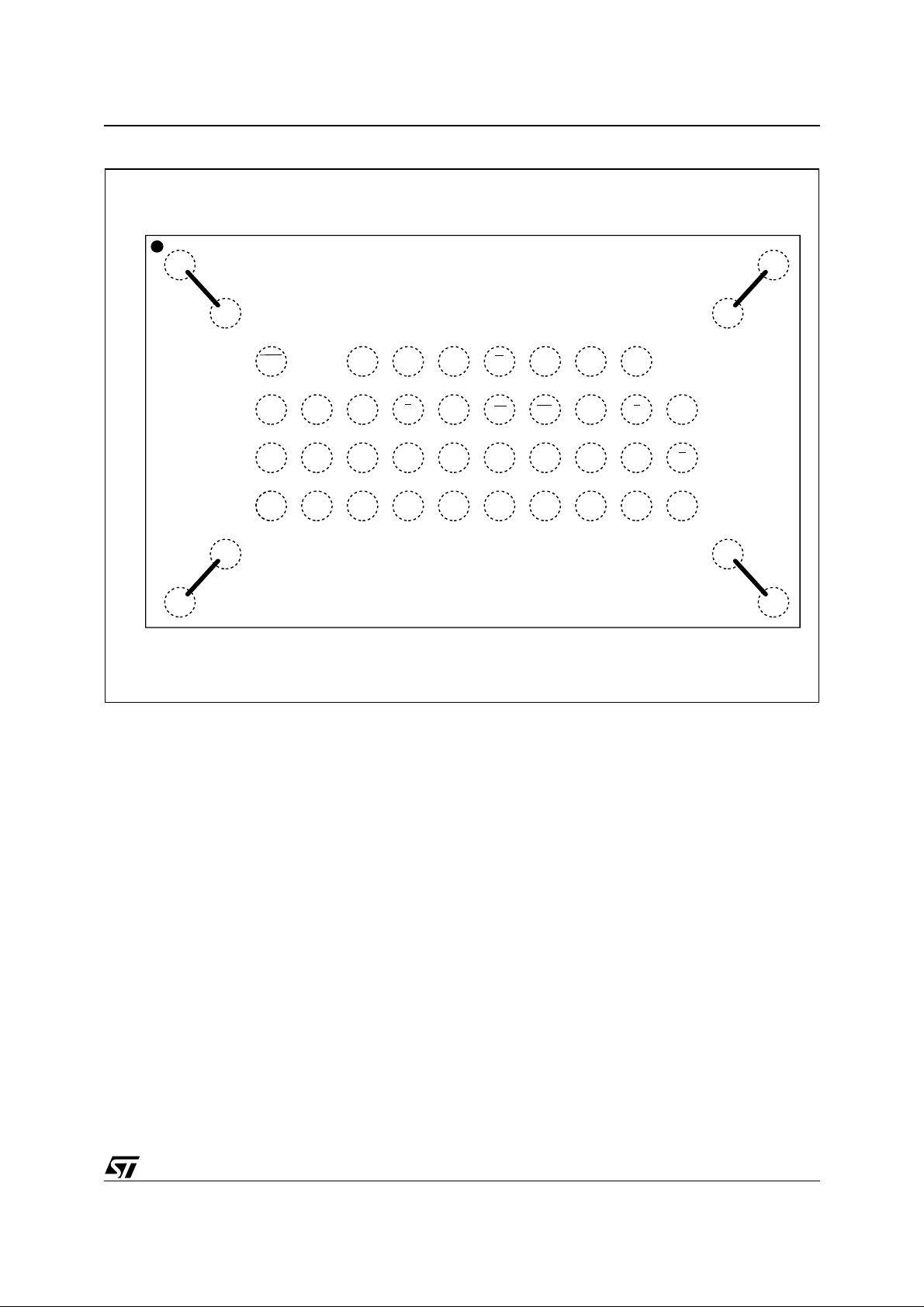
Figure 3. µBG A Co nn e ct i ons (Top view through pack a ge)
M59MR032C, M59MR032D
87654321
A
B
C
D
E
F
G
H
DU
DU
DU
DU
DDQ
SS
SS
SS
KWAIT
ADQ13 ADQ12
V
ADQ14ADQ15
DD
WV
WPRPBINVLA20A16V
ADQ2ADQ3ADQ6ADQ7V
ADQ10ADQ11ADQ4ADQ5V
V
109
A17
A19
PP
A18
ADQ8
ADQ9
V
ADQ1
DDQ
1211
DU
V
E
SS
G
ADQ0
DU
1413
DU
DU
AI90111
3/49
M59MR032C, M59MR032D
Table 1. Signal Names
A16-A20 Address Inputs
ADQ0-ADQ15
E
G
W
RP
WP
K Burst Clock
L
WAIT
BINV Bus Invert
V
DD
V
DDQ
V
PP
V
SS
Data Input/Outputs or Address
Inputs, Command Inputs
Chip Enable
Output Enable
Write Enable
Reset/Power-down
Write Protect
Latch Enable
Wait Data in Burst Mode
Supply Voltage
Supply Voltage for Input/Output
Buffers
Optional Supply Voltage for
Fast Program & Erase
Ground
DESCRIPTION
The M59MR032 is a 32 Mbit non-volatile Flash
memory that m ay be erased electrically a t block
level and programmed in-system on a Word-byWord basis using a 1.65V to 2.0V V
supply for
DD
the circuitry. For Program and Erase operations
the necessary high voltages are g enerated internally. The device supports synchronous burst read
and asynchronous page mode read from all the
blocks of the memory array; at power-up the device is configured for page mode read. In synchronous burst mode, a new data is output at each
clock cycle for frequencies up to 54MHz.
The array matrix organization allows each block to
be erased and reprogrammed without affecting
other blocks. All blocks are protected against programming and erase at Power-up. Blocks can be
unprotected to make changes in the application
and then reprotected.
Instructions for Read/Reset, Auto Select, Write
Configuration Register, Programming, Block
Erase, Bank Erase, Erase Suspend, Erase Resume, Block Protect, Block Unprotect, Block Locking, CFI Query, are written to the memory through
a Command Interface (C.I.) using standard microprocessor write timings.
The memory is offered in LFBGA54 and µBGA46,
0.5 mm ball pitch packages and it is supplied wit h
all the bits erased (set to ’1’).
DU Don’t Use as Internally Connected
Table 2. Absolute Maximum Ratings
Symbol Parameter Value Unit
T
A
T
BIAS
T
STG
(3)
V
IO
, V
V
DD
DDQ
V
PP
Note: 1. Except for the ra ting "Oper at i ng Temperat ure Range", stresse s above those listed i n the Tabl e "Absolute M aximum Ratings" may
cause permanent damage to the device. These are stress ratings only and operation of the device at these or any other conditions
above those indi cated in t he Operating secti ons of thi s specif i cation is not imp l i ed. Exposure to Ab solute Maxi m um Rati ng condi tions for extended per iods may aff ect device reliabilit y. Refer also to the STMicroel ectronics SURE Program an d other relevan t qual ity docum en ts .
2. Depends on range.
3. Minimum Vol tage may undershoot to –2V during tr ansition and for less tha n 20ns.
Ambient Operating Temperature
Temperature Under Bias –40 to 125 °C
Storage Temperature –55 to 155 °C
Input or Output Voltage
Supply Voltage –0.5 to 2.7 V
Program Voltage –0.5 to 13 V
(1)
(2)
–40 to 85 °C
–0.5 to V
DDQ
+0.5
V
4/49
M59MR032C, M59MR032D
Organization
The M59MR032 is org anized as 2Mbit by 16 bit s.
The first sixteen address lines are multiplexed with
the Data Input/Output signals on the m ultiplexed
address/data bus ADQ0-ADQ15. The remaining
address lines A16-A20 are the MSB addresses.
Memory control is provided by Chip Enable E
put Enable G
and Write Enable W inputs.
, Out-
The clock K input synchronizes the memory to the
microprocessor during burst read.
Reset RP
is used to reset all the memory circuitry
and to set the chip in power-down mode if this
function is enabled by a proper setting of the Configuration Register. Erase and Program operations
are controlled by an internal Program/Erase Controller (P/E.C.). Status Register data output on
ADQ7 provide s a Data Pollin g signal, ADQ6 and
ADQ2 provide Toggle signals and ADQ5 provides
error bit to indicate the state of the P/E.C operations. WAIT
output indicates to the microprocessor
the status of the memory during the burst mode
operations.
Table 3. Bank Size and Sectorization
Bank Size Parameter Blocks Main Blocks
Bank A 8 Mbit 8 blocks of 4 KWord 15 blocks of 32 KWord
Memory Blocks
The device features asymmetrically blocked architecture. M59MR032 has an array of 71 blocks and
is divided into two banks A and B, prov iding D ual
Bank operations. While programming or erasing in
Bank A, read operations are possible into Bank B
or vice versa. The memory also features an erase
suspend allowing to read or program in another
block within the same bank. Once suspended the
erase can be resumed. The Bank Size and Sectorization are summarized in Table 8. Parameter
Blocks are located at the top of the m emory address space for the M59MR032C, and at the bo ttom for the M59MR032D. The memory maps are
shown in Tables 4, 5, 6 and 7.
The Program and Erase operation s are managed
automatically by the P/E.C. Block protection
against Program or Erase provides additional data
security. Instructions are provided to protect or unprotect any block in the application. A second register locks the protection status while WP
is low
(see Block Lockin g description). All blocks are protected and unlocked at Power-up.
Bank B 24 Mbit - 48 blocks of 32 KWord
5/49
M59MR032C, M59MR032D
Table 4. Bank A, Top Boot Block Addresses
M59MR032C
#
22 4 1FF000h-1FFFFFh
21 4 1FE000h-1FEFFFh
20 4 1FD000h-1FDFFFh
19 4 1FC000h-1FCFFFh
18 4 1FB000h-1FBFFFh
17 4 1FA000h-1FAFFFh
16 4 1F9000h-1F9FFFh
15 4 1F8000h-1F8FFFh
14 32 1F0000h-1F7FFFh
13 32 1E8000h-1EFFFFh
12 32 1E0000h-1E7FFFh
11 32 1D8000h-1DFFFFh
10 32 1D0000h-1D7FFFh
9 32 1C8000h-1CFFFFh
8 32 1C0000h-1C7FFFh
7 32 1B8000h-1BFFFFh
6 32 1B0000h-1B7FFFh
5 32 1A8000h-1AFFFFh
4 32 1A0000h-1A7FFFh
3 32 198000h-19FFFFh
2 32 190000h-197FFFh
1 32 188000h-18FFFFh
0 32 180000h-187FFFh
Size
(KWord)
Address Range
Table 5. Bank B, Top Boot Block Addresses
M59MR032C
#
47 32 178000h-17FFFFh
46 32 170000h-177FFFh
45 32 168000h-16FFFFh
44 32 160000h-167FFFh
43 32 158000h-15FFFFh
42 32 150000h-157FFFh
41 32 148000h-14FFFFh
40 32 140000h-147FFFh
39 32 138000h-13FFFFh
Size
(KWord)
Address Range
38 32 130000h-137FFFh
37 32 128000h-12FFFFh
36 32 120000h-127FFFh
35 32 118000h-11FFFFh
34 32 110000h-117FFFh
33 32 108000h-10FFFFh
32 32 100000h-107FFFh
31 32 0F8000h-0FFFFFh
30 32 0F0000h-0F7FFFh
29 32 0E8000h-0EFFFFh
28 32 0E0000h-0E7FFFh
27 32 0D8000h-0DFFFFh
26 32 0D0000h-0D7FFFh
25 32 0C8000h-0CFFFFh
24 32 0C0000h-0C7FFFh
23 32 0B8000h-0BFFFFh
22 32 0B0000h-0B7FFFh
21 32 0A8000h-0AFFFFh
20 32 0A0000h-0A7FFFh
19 32 098000h-09FFFFh
18 32 090000h-097FFFh
17 32 088000h-08FFFFh
16 32 080000h-087FFFh
15 32 078000h-07FFFFh
14 32 070000h-077FFFh
13 32 068000h-06FFFFh
12 32 060000h-067FFFh
11 32 058000h-05FFFFh
10 32 050000h-057FFFh
9 32 048000h-04FFFFh
8 32 040000h-047FFFh
7 32 038000h-03FFFFh
6 32 030000h-037FFFh
5 32 028000h-02FFFFh
4 32 020000h-027FFFh
3 32 018000h-01FFFFh
2 32 010000h-017FFFh
1 32 008000h-00FFFFh
0 32 000000h-007FFFh
6/49
M59MR032C, M59MR032D
Table 6. Bank B, Bottom Boot Blo ck Addresses
M59MR032D
#
47 32 1F8000h-1FFFFFh
46 32 1F0000h-1F7FFFh
45 32 1E8000h-1EFFFFh
44 32 1E0000h-1E7FFFh
43 32 1D8000h-1DFFFFh
42 32 1D0000h-1D7FFFh
41 32 1C8000h-1CFFFFh
40 32 1C0000h-1C7FFFh
39 32 1B8000h-1BFFFFh
38 32 1B0000h-1B7FFFh
37 32 1A8000h-1AFFFFh
36 32 1A0000h-1A7FFFh
35 32 198000h-19FFFFh
34 32 190000h-197FFFh
33 32 188000h-18FFFFh
32 32 180000h-187FFFh
31 32 178000h-17FFFFh
30 32 170000h-177FFFh
29 32 168000h-16FFFFh
28 32 160000h-167FFFh
27 32 158000h-15FFFFh
26 32 150000h-157FFFh
25 32 148000h-14FFFFh
24 32 140000h-147FFFh
23 32 138000h-13FFFFh
22 32 130000h-137FFFh
21 32 128000h-12FFFFh
20 32 120000h-127FFFh
19 32 118000h-11FFFFh
18 32 110000h-117FFFh
17 32 108000h-10FFFFh
16 32 100000h-107FFFh
15 32 0F8000h-0FFFFFh
14 32 0F0000h-0F7FFFh
13 32 0E8000h-0EFFFFh
12 32 0E0000h-0E7FFFh
Size
(KWord)
Address Range
11 32 0D8000h-0DFFFFh
10 32 0D0000h-0D7FFFh
9 32 0C8000h-0CFFFFh
8 32 0C0000h-0C7FFFh
7 32 0B8000h-0BFFFFh
6 32 0B0000h-0B7FFFh
5 32 0A8000h-0AFFFFh
4 32 0A0000h-0A7FFFh
3 32 098000h-09FFFFh
2 32 090000h-097FFFh
1 32 088000h-08FFFFh
0 32 080000h-087FFFh
Table 7. Bank A, Bottom Boot Blo ck Addresses
M59MR032D
#
22 32 078000h-07FFFFh
21 32 070000h-077FFFh
20 32 068000h-06FFFFh
19 32 060000h-067FFFh
18 32 058000h-05FFFFh
17 32 050000h-057FFFh
16 32 048000h-04FFFFh
15 32 040000h-047FFFh
14 32 038000h-03FFFFh
13 32 030000h-037FFFh
12 32 028000h-02FFFFh
11 32 020000h-027FFFh
10 32 018000h-01FFFFh
9 32 010000h-017FFFh
8 32 008000h-00FFFFh
7 4 007000h-007FFFh
6 4 006000h-006FFFh
5 4 005000h-005FFFh
4 4 004000h-004FFFh
3 4 003000h-003FFFh
2 4 002000h-002FFFh
1 4 001000h-001FFFh
0 4 000000h-000FFFh
Size
(KWord)
Address Range
7/49

M59MR032C, M59MR032D
SIGNAL DESCRIPTIONS
See Figure 1 and Table 1.
Address Inputs or Data Input/Output (ADQ0ADQ15). When Chip Enable E
put Enable G
is at VIH the multiplexe d address/
is at VIL and Out-
data bus is used to input addresses for the memory array, data to be programmed in the memory array or commands to be written to the C.I. The
address inputs for the memory array are latched
on the rising edge of Latch Enable L
latch is transparent when L
is at VIL. Both input
. The address
data and commands are latched on the rising edge
of Write Enable W
put Enable G
. When Chip Enable E and Out-
are at VIL the address/data bus outputs data from the Memory Array, the Electronic
Signature Manufacturer or Device codes, the
Block Protection status the Configuration Register
status or the Status Register Data Polling bit
ADQ7, the Toggle Bits ADQ6 and ADQ2, the Error
bit ADQ5. The address/data bus is high impedance when the chip is deselected, Output E nable
G
is at VIH, or RP is a t VIL.
Address Inputs (A16-A20). The five MSB addresses of the m emory array are latched on t he
rising edge of Latch Enable L
Chip Enable (E
). The Chip Enable input acti-
.
vates the memory control logic, input buffers, decoders and sense amplifiers. E
at VIH deselects
the memory and red uces the power consumption
to the standby level. E
can also be used to control
writing to the command register and to the memory array, while W
Output Enable (G
remains at VIL.
). The Output Enable gates the
outputs through the data buffers during a read operation. When G
is at VIH the outputs are High im-
pedance.
Write Enable (W
). This input controls writing to
the Command Register and Data latches. Data are
latched on the rising edge of W
.
Write Protect (WP
). This input gives an addition-
al hardware protection level against program or
erase when pulled at V
, as described in the Block
IL
Lock instruction description.
Reset/Power-down Input (RP
). The RP input
provides hardware reset of the memory, and/or
Power-down functions, depending on the Configuration Register status. Reset/Power-down of the
memory is achieved by pulling RP
least t
. When the reset pul se is given, if the
PLPH
to VIL for at
memory is in Read, Erase Suspend Read or
Standby, it will output new valid data in t
ter the rising edge of RP
. If the memory is in Erase
PHQ7V1
af-
or Program modes, the oper ation will be aborted
and the reset recovery will take a maximum of
. The memory will recover from Power-
t
PLQ7V
down (when enabled) in t
edge of RP
. Exit from Reset/Power-down changes
PHQ7V2
after the rising
the contents of the configuration register bits 14
and 15, setting the memory in asynchronous page
mode read and power save func tion disabled. All
blocks are protected and unlocked after a Reset/
Power-down. See Tables 29, 31 and Figure 14.
Latch Enable (L
). L latches the address bits
ADQ0-ADQ15 and A16-A20 on its rising edge.
The address latch is transparent when L
is at V
and it is inhibited when L is at VIH.
Clo c k (K). The clock input synchronizes the
memory to the microcontroller during burst mode
read operation; the address is latched on a K edge
(rising or falling, according to the configuration settings) when L
is at VIL. K is don’t care during asyn-
chronous page mode read and in write operations.
Wait (WAIT
). WAIT i s an output signal used dur-
ing burst mode read, indicating whet her the data
on the output bus are valid or a wait state must be
inserted. This output is high impedance when E
G
are high or RP is at VIL, and can be configured
or
to be active during the wait cycle or one clock cycle in advance.
IL
8/49

M59MR032C, M59MR032D
Bus Invert (BINV). BINV is an input/output signal
used to reduce the amount of power needed to
switch the external address/data bus. The power
saving is achieved by inverting the dat a output on
ADQ0-ADQ15 every time this gives an advantage
in terms of number of toggling bits. In burst mode
read, each new data output from the memory is
compared with the previous data. If the number of
transitions required on the data bus is in excess of
8, the data is inverted and the BINV signal will be
driven by the memory at V
to inform the receiv-
OH
ing system that dat a must be inverted b efore any
further processing. By doing so, the act ual transitions on the data bus will be less than 8. In a similar way, when a command is given, BINV may be
driven by the s ystem a t V
to inform the memory
IH
that the data must be inverted.Like the other input/
output pins, BINV is high impedance when the
chip is deselected, output enable G
is at VIH or RP
is at VIL; when used as an input, BINV must follow
the same setup and hold timi ngs of the data inputs.
V
and V
DD
Supply Voltage (1.65V to 2.0V).
DDQ
The main power supply for all operations (Read,
Program and Erase). V
and V
DD
must be at
DDQ
the same voltage.
V
Program Supply Voltage (12V). VPP is
PP
both a control input and a power supply pin. T he
two functions are selected by the voltage range
applied to the pin; if V
range (0 to 2V) V
PP
is kept in a low vo ltage
PP
is seen as a control input, and
the current absorption is limited to 5µA (0.2µA typical). In this case with V
= VIL we obtain an ab-
PP
solute protection against program or erase; with
= V
V
PP
these functions are enabled. VPP val-
PP1
ue is only sampled during program or erase write
cycles; a change in its value after the operation
has been started does not have any effect and
program or erase are carried on regularly. If V
used in the 11.4V to 12. 6V range (V
) then the
PP2
PP
is
pin acts as a power suppl y. This supply voltage
must remain stable as long as program or eras e
are finished. In read mode the current sunk is less
then 0.5mA, while during program and erase operations the current may increase up to 10mA.
V
Ground. VSS is the reference for al l the vol t-
SS
age measurements.
9/49
M59MR032C, M59MR032D
DEVICE OPERATIONS
The following operations can be performed using
the appropriate bus cycles: Address Latch, Read
Array (Random, and Page Modes), Write command, Output Disable, Standby, Reset/Powerdown and Block Locking. See Table 8.
Address Latch. In asynchronous operation, the
address is latched on the rising edge of L
burst mode, the address is latched either by L
input; in
going high or with a rising/fallin g edge of K , de pending on the clock configuration.
Read. Read operations are used to output the
contents of the Memory Array, the Electronic Signature, the Status Register, the CFI, the Block
Protection Status, the Configuration Register status and the Security Code.
Table 8. User Bus Operations
Operation E G W RP WP ADQ0-ADQ15
Write
Output Disable
Standby
Reset / Power-down X X X
Block Locking
Note: 1. X = Don’t care.
(1)
V
IL
V
IL
V
IH
V
IL
V
IH
V
IH
XX
XX
Read operation of the Memory Array may be performed in asynchronous page mode or synchronous burst mode. In asynchronous page mode
data is internally read and stored in a page buffer.
The page has a size of 4 words and is addres sed
by ADQ0 and ADQ1 address inputs.
According to the device configuration the following
Read operations: Electronic Signature - Status
Register - CFI - Block Protection Status - Configuration Register Status - Security Code must be accessed as asynchronous read or as single
synchronous burst mode (see Figure 4). Both Chip
Enable E
and Output Ena ble G must be at VIL in
order to read the output of the memory.
V
IL
V
IH
V
IH
V
IH
V
IH
V
IL
V
IH
V
IH
V
IH
V
IH
V
IH
V
IL
Data Input
Hi-Z
Hi-Z
Hi-Z
X
Table 9. Read Electronic Signature (AS and Read CFI instructions)
Code Device E
Manufacturer Code
M59MR032C
Device Code
M59MR032D
Note: 1. Addresses are l atched on the ri sing edge of L input.
V
IL
V
IL
V
IL
Table 10. Read Block Protection (AS and Read CFI instructions)
Block Status E
Protected and
unlocked
Unprotected and
unlocked
Protected and locked
Unprotected and
(2)
locked
Note: 1. Addresses are l atched on the ri sing edge of L input.
2. A locked blo ck can be unprot ected only wit h WP
V
IL
V
IL
V
IL
V
IL
G W A0-A7 A8-A11 A12-A20 Data
V
V
V
V
V
IL
IL
IL
IL
IH
V
IH
V
IH
V
IH
at V
G W A0-A7 A8-A20 Data
V
IL
V
IL
V
IL
V
IH
V
IH
V
IH
(1)
02h Don’t Care Block Address 0001
02h Don’t Care Block Address 0000
02h Don’t Care Block Address 0003
02h Don’t Care Block Address 0002
IH.
(1)
00h Don’t Care 0020h
01h Don’t Care 00A4h
01h Don’t Care 00A5h
10/49
M59MR032C, M59MR032D
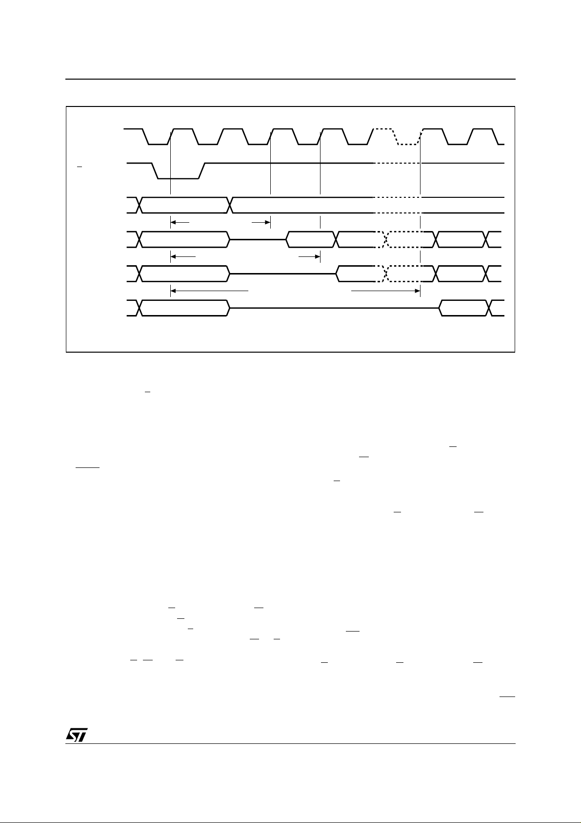
Figure 4. Read Operation Sequence wh en CR15 = 0 (excluding Read Me mory Array)
K
L
A16-A20
ADQ0-ADQ15
ADQ0-ADQ15
ADQ0-ADQ15
VALID ADDRESS
CONF. CODE 2
VALID ADDRESS VALID DATA NOT VALID
CONFIGURATION CODE 3
VALID ADDRESS VALID DATA
CONFIGURATION CODE 6
VALID ADDRESS VALID DATA
Burst Read. The device also supports a burst
read. In this mode, an address is first latched on
the rising edge of L
or K (or fallin g edge of K, according to configuration settings); after a configurable delay of 2 to 6 clock cycles a new data is
output at each clock cycle. The burst sequence
may be configured for linear o r interleaved order
and for a length of 4, 8 words or for continuous
burst mode.
A WAIT
signal may be asserted to indicate to the
system that an output delay will occur.
This delay will depend on the starting address of
the burst sequence; the worst case delay will occur when the sequence is crossing a 32 word
boundary and the starting address was at the end
of a four word boundary. See the Write Configuration Register (CR) Instruction for more details on
all the possible settings for the synchronous burst
read.
Write. Write operations are used to give I nstruction Commands to the memory or to latch Input
Data to be programmed. A write operation is initiated when Chip Enable E
with Output Enable G at VIH. Addresses are
at V
IL
latched on the rising edge of L
put Data are latched on the rising edge of W
and Write Enable W are
. Commands and In-
or E
whichever occurs first. Noise pulses of less than
5ns typical on E
, W and G signals do not start a
write cycle. Write operations are asynchronous
and clock is ignored during write.
Dual Bank Operations. The Dual Bank allows to
read data from one bank of memory while a pro-
NOT VALID
NOT VALID
AI90112
gram or erase operation is in progress in the other
bank of the memory. Read and Write cycles can
be initiated for simultaneous operations in different
banks without any d elay. Status Register du ring
Program or Erase must be monitored using an address within the bank being modified.
Output Disa bl e . The data outputs are high impedance when the Output Enable G
Write Enable W
at VIH.
is at VIH with
Standby. The mem ory is in standby when C hip
Enable E
is at VIH and the P/E.C. is idle. The power consumption is reduced to the standby level
and the outputs are high impedance, independent
of the Output Enable G
or Write Enable W input s.
Automatic Standby. When in Read mode, after
150ns of bus inactivity and when CMOS levels are
driving the addresses, the chip automatically enters a pseudo-standby mode where consumption
is reduced to the CMOS standby value, while outputs still drive the bus. The automatic standby feature is not available when the device is configured
for synchronous burst mode.
Power-down. The memory is in Power-down
when the Configuration Register is set for Powerdown and RP
is at VIL. The power consumption is
reduced to the Power-down level, and Outputs are
in high impedance, independent of the Chip Enable E
, Output Enable G or Write Enable W inputs.
Block Locking. Any combination of blocks can
be temporarily protected against Program or
Erase by setting the lock register and pulling WP
to VIL (see Block Lock instruction).
11/49
M59MR032C, M59MR032D
INSTRUCTIONS AND COMMANDS
Seventeen instructions are defined (see Table
17), and the internal P/E.C. automatically handles
all timing and verification of the Program and
Erase operations. The Status Register Dat a Polling, Toggle, Error bits can be read at any time, during programming or erase, to monitor the progress
of the operation.
Instructions, made up of one or more com mands
written in cycles, can be given to the Program/
Erase Controller through a Command Interface
(C.I.). The C.I. latches comma nds written to the
memory. Commands are made of address and
data sequences. Two Coded Cycles unlock the
Command Interface. They are followed by an input
command or a confirmation command. The Coded
Sequence consists of writing the dat a AAh at the
address 555h during the f irst cycle and the data
55h at the address 2AAh during the second cycle.
Instructi ons a re co mpose d of up to si x cycles. The
first two cycles input a Coded Sequence to the
Command Interface which is common to all instructions (see Table 17). T he third cycle inputs
the instruction set-up command. Subseq uent cycles output the addressed data, Elect ronic Signature, Block Protection, Configuration Register
Status or CFI Query for Read operations. In order
to give additional data protection, the instructions
for Block Erase and Bank Erase require further
command inputs. For a Program instruction, the
fourth command cycle inputs the address and data
to be programmed. For a Double Word Programming instruction, the fourth and fifth co mmand cycles input the address and data to be
programmed. For a Block Eras e and Bank Erase
instructions, the fourth and fifth cycles input a further Coded Sequence before the Erase confirm
command on the sixth cycle. Any combination of
blocks of the same memory bank can be erased.
Erasure of a memory block may be suspended, in
order to read data from another block or to program data in another block, and then resumed.
When power is first applied the command interface
is reset to Read Array.
Command sequencing must be followed exactly.
Any invalid combination of commands will reset
the device to Read Array. The inc reased number
of cycles has been chosen to ensure maximum
data security.
Read/Reset (RD) Instruction. The Read/Reset
instruction consists of one write cycle giving the
command F0h. It can be optionally preceded by
the two Coded Cycles. Subsequent read operations will r ead the memory array a ddressed and
output the data read. The Reset com mand does
not affect the configurati on of unprotected blo cks
and the Configuration Register status. Read/Reset Instruction is ignored when program or erase is
in progress.
CFI Query (RCFI) Instruction. Common Flash
Interface Query mode is entered writing 98h at address 55h. The CFI data structure gives information on the device, such as the sectorization, the
command set and some el ectrical specifications.
Tables 19, 20, 21 and 22 show the addresses
used to retrieve each data. The CFI data structure
contains also a se curity area; in this section, a 64
bit unique security number, organ ized by word, is
written starting at address 81h. This area can be
accessed only in read mode by the final user and
there are no ways of changing the code after it has
been written by ST. Write a read instruction (RD)
to return to Read Array mode.
Table 11. Commands
Hex Code Command
00h Bypass Reset
10h Bank Erase Confirm
20h Unlock Bypass
30h Block Erase Resume/Confirm
40h Double Word Program
Block Protect, or
60h
80h Set-up Erase
90h
98h CFI Query
A0h Program
B0h Erase Suspend
F0h Read Array/Reset
Block Unprotect, or
Block Lock, or
Write Configuration Register
Read Electronic Signature, or
Block Protection Status, or
Configuration Register Status
12/49
M59MR032C, M59MR032D
Auto Select (AS) Instruction. This instruc-
tion uses two Coded Cycles followed by one write
cycle giving the command 90h to address 555h for
command set-up. A subsequent read will output
the Manufacturer or the Device Code (Electronic
Signature), the Block Protection status or the Configuration Register status depending on the levels
of ADQ0 and ADQ1 (see Tables 9, 10 and 11).
The Electronic Signature can be read from the
memory allowing programming equipment or applications to automatic ally match their interface to
the characteristics of M59MR032. The Manu facturer Code is output when the address lines ADQ0
and ADQ1 are at V
when ADQ0 is at V
, the Device Code is output
IL
with ADQ1 at VIL.
IH
The codes are output on ADQ0-ADQ7 with ADQ8ADQ15 at 00h. The A S ins truction also allows the
access to the Block Protection Status. After giving
the AS instruction, ADQ0 is set to V
, while A12-A20 define the address of the
at V
IH
with ADQ1
IL
block to be verified (see Table 10). The AS Instruction finally allows the access to the Configuration
Register status if both ADQ0 and ADQ1 are set to
V
; refer to Table 12 for configuration register de-
IH
scription.
A reset command puts the device in Read Array
mode.
Write Configuration Register (CR) Instruction. This instruction uses t wo Coded Cyc les fol-
lowed by one write cycle giving the command 60h
to address 555h. A further write cycle giving the
command 03h writes the cont ents of address bi ts
ADQ0-ADQ15 to bits CR15-CR0 of the configuration register. At Power-up the Configu ration Register is set to asynchronous Read mode, Powerdown disabled and bus invert (power save function) disabled.
A description of the effects of each configuration
bit is given in Table 12.
Table 12. Read Configuration Register (AS and Read CFI instructions)
Configuration Register Function
Read mode
CR15
CR14
CR13-CR11
CR10
CR9
CR8
CR7
CR6
CR5-CR3 Reserved
CR2-CR0
0 = Burst mode read
1 = Page mode read (default)
Bus Invert configuration (power save)
0 = disabled (default)
1 = enabled
X-Latency
010 = 2 clock latency
011 = 3 clock latency
100 = 4 clock latency
101 = 5 clock latency
110 = 6 clock latency
Power-down configuration
0 = power-down disabled (default)
1 = power-down enabled
Data hold configuration
0 = data output at every clock cycle
1 = data output every 2 clock cycles
Wait configuration
0 = WAIT
1 = WAIT
Burst order configuration
0 = Interleaved
1 = Linear
Clock configuration
0 = Address latched and data output on the falling clock edge.
1 = Address latched and data output on the rising clock edge.
Burst length
001 = 4 word burst length
010 = 8 word burst length
111 = Continuous burst mode (requires CR7 = 1)
is active during wait state
is active one data cycle before wait state
13/49
M59MR032C, M59MR032D
Table 13. X-Latency Configuration
Configuration Code
2 25MHz 20MHz
3 40MHz 30MHz
4 54MHz 40MHz
(1)
5
(1)
6
Note: 1. Configurati on codes 5 and 6 may be used only in conjunct i on with configuration bit CR9 set at “1” (one data ever y 2 clock cycles).
100ns 120ns
66MHz 50MHz
– 60MHz
Figure 5. X-L at ency Configu ra ti on Sequenc e
K
L
Input Frequency
A16-A20
ADQ0-ADQ15
ADQ0-ADQ15
ADQ0-ADQ15
VALID ADDRESS
CONF. CODE 2
VALID ADDRESS VALID DATA VALID DATA
CONFIGURATION CODE 3
VALID ADDRESS VALID DATA
CONFIGURATION CODE 6
VALID ADDRESS VALID DATA
– Read mode (CR15). The device supports an
asynchronous page mode and a synchronous
burst mode. In asynchrono us page mode, the
default at power-up, data is internally read and
stored in a buffer of 4 words selected by ADQ0
and ADQ1 address inputs. In synchronous burst
mode, the device latches the starting address
and then outputs a sequence of data which depends on the configuration register settings.
– Bus Invert configuration (CR14). This regis-
ter bit is used to enable the BINV pin functionality. BINV functionality depends upon
configuration bits CR14 and CR15 (see Table
12 for configuration bits definition) as shown in
Table 14.
VALID DATA
VALID DATA
AI90113
As output p in BINV is active only wh en enabled
(CR14 = 1) in Read Array burst mode (CR15 = 0).
As input pin BINV is active only when enabled
(CR14 = 1). BINV is ignored when ADQ0ADQ15 lines are used as address inputs (addresses must not be inverted).
Table 14. BINV Configuration Bits
CR15 CR14
00X0
0 1 Active Active
10X0
1 1 Active 0
BINV
IN OUT
14/49
M59MR032C, M59MR032D
Table 15. Burst Order and Length Configuration
Starting
Address
0 0-1-2-3 0-1-2-3 0-1-2 -3-4-5 -6-7 0-1-2-3-4-5-6-7 0-1-2 -3-4-5 ...
1 1-2-3-0 1-0-3-2 1-2-3 -4-5-6 -7-0 1-0-3-2-5-4-7-6 1-2-3 -4-5-6 ...
2 2-3-0-1 2-3-0-1 2-3-4 -5-6-7 -0-1 2-3-0-1-6-7-4-5 2-3-4 -5-6-7 ...
3 3-0-1-2 3-2-1-0 3-4-5 -6-7-0 -1-2 3-2-1-0-7-6-5-4 3-4-5 -6-7-8 ...
...
7 7-4-5-6 7-6-5-4 7-0-1 -2-3-4 -5-6 7-6-5-4-3-2-1-0 7-8-9-10-11...
...
28 28-29-30-31- 32...
29 29-30-31-WAIT-32...
30 30-31-WAIT-WAIT-32...
31 31-WAIT-WAIT-WAIT-32...
Linear Interle aved L inear Interleaved
4 Words 8 Words
Continuous Burst
– X-Latency (CR13-CR11). These configuration
bits define the number of clock cycles ela psing
going low to valid data available in b urst
from L
mode. The correspondence between X-Latency
settings and the sustainable clock freq uencies
is given in Table 13 and Figure 5.
– Power-down configuration (CR10). The RP
pin may be configured to give a very low power
consumption when driven low (power-down
state). In power-down the I
supp ly cu rre nt is
CC
reduced to a typical figure of 2µA; if this function
is disabled (default at power-up) the RP
pin
causes only a reset of the device and the supply
current is the stand-by value. The recovery time
after a RP
pulse is significantly longer (50µs vs.
150ns) when power-down is enabled.
– Data hold configuration (CR9). In burst
mode this register bit determines if a new data
is output at each clock cycle or every 2 clock cycles.
– Wait configuration (CR8). In burst mode
indicates whether the data on the ou tput
WAIT
bus are valid or a wait s tate must be inserted.
The configuration bit determines if WAIT
will be
asserted one clock cycle before the wait state or
during the wait state (see Figure 10).
– Burst order configuration (CR7). See Table
15 for burst order and length.
– Clock c o nf ig uration (CR 6) . In burst mode de-
termines if address is latched and data is output
on the risin g o r falling edge of th e clo ck.
– Burst length (CR2-CR0). In burst mode deter-
mines the number of words output by the memory. It is possible to have 4 words, 8 words or a
continuous burst mode, in which all the words in
bank A or bank B are read sequentia lly. In continuous burst mode the burst sequenc e is in terrupted at the end of each o f the two banks or
when a suspended block is reached. In continuous burst mode it may happen that the memory
will stop the data output flow for a few clock cycles; this event is signaled by WAIT
going low
until the output flow is resumed. The initial address determines if the output delay will occur
as well as its duration. I f t he st arting a ddres s is
aligned to a four word boundary no wait sta tes
will be needed. If the starting address is shi fted
by 1,2 or 3 pos itions f rom t he four word b oundary, WAIT
will be asserted for 1,2 or 3 clock cy-
cles (2,4, 6 cycles if CR9 is set at “1”) when the
burst sequence is crossing the first 32 word
boundary. WAIT
will be asserted only once dur-
ing a continuous burst access. See also Table
15.
Enter Bypass Mode (EBY) Instruction. This instruction uses the two Coded cycles f ollowed by
one write cycle giving the command 20h to address 555h for mode set-up. Once in Bypass
mode, the device will accept the Exit Bypass
(XBY) and Program or Double Word Program in
Bypass mode (PGBY, DPGBY) commands. The
Bypass mode allows to reduce the overall programming time when large memory arrays need to
be programmed.
Exit B y pa ss Mode (XBY) Ins t r uc tion . This instruction uses two write cycles. The first inputs to
the memory the command 90h and the second inputs the Exit Bypass mode confirm (00h). After the
XBY instruction, the device resets to Read Memory Array mode.
15/49
 Loading...