

1 Mbit (64Kb x16, Burst) Low Voltage Flash Memory
■ 2.7 to 3. 6V SUPPLY VOLTAGE f or PROGRAM,
ERASE and READ OPERATIONS
■ SEQUENTIAL CYCLE TIME: 25ns
■ RANDOM ACCESS TIME
■ PROGRAMMING TIME: 10µs typical
■ INTERLEAVED ACCESS TIME: 16ns
■ CONTINUOUS MEMORY INTERLEAVING
– Unlimited Linear Access Data Output
■ PROGRAM/ERASE CONTROLLER (P/E.C.)
– Program Word-by-Word
– Status Register bits
■ LOW POWER CONSUMPTION
– Stand-by and Automatic Stand-by
■ 100,000 PROGRAM/ERASE CYCL ES
■ 20 YEARS DATA RETENTI ON
– Defectivity below 1ppm/year
■ ELECTRONIC SIGNATURE
– Manufacturer Code: 20h
– Device Code: C1h
DESCRIPTION
The M59BW102 is a non-volatile memory that may
be erased electrically at the chip level and programmed in-system on a Word-by-Word basis using only a single 3V V
Erase operations the necessary high voltages are
generated internally. The de vice can also be programmed in standard programmers.
The device can be programmed and erased over
100,000 cycles.
Instructions for Read/Reset, Auto Select for reading the Electronic Signature, Programming and
Chip Erase are written to the device in cycles of
commands to a Command Interface using standard microprocessor write timings. The
M59BW102 features an interleaved access modality which allows extremely fast access time.
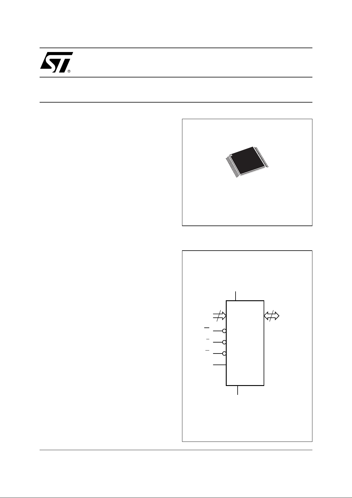
The device is offered in TSOP40 (10 x 14mm)
package.
supply. For Program and
CC
TSOP40 (N)
10 x 14mm
Figure 1. Logic Diagram
V
CC
16
A0-A15
W
E
G
ALE
M59BW102
V
SS
M59BW102
PRELIMINARY DATA
16
DQ0-DQ15
AI02763B
March 2000
This is preliminary information on a new product now in development or undergoing evaluation. Details are subject to change without notice.
1/24
M59BW102
Figure 2. TSOP Connections
A9
A10
A11
A12
A13
A14
A15
ALE
W
V
CC
NC
DQ15
DQ14
DQ13
DQ12
DQ11
DQ10
DQ9
DQ8
1
10
M59BW102
11
E
20 21
AI02764B
40
31
30
V
SS
A8
A7
A6
A5
A4
A3
A2
A1
A0
G
DQ0
DQ1
DQ2
DQ3
DQ4
DQ5
DQ6
DQ7
V
SS
Organization
The M59BW102 is organized as 64K x16 bits. The
memory uses the addre ss inputs A0-A 15 and the
Data Inputs/Outputs DQ0-DQ15. Memory control
is provided by Chip Enable E
Address Latch Enable ALE and Write Enable W
, Output Enable G,
in-
puts.
Erase and Program operations are controlled by
an internal Program/Erase Controller (P/E.C.).
Status Register data output on DQ7 provides a
Data Polling signal, and DQ6 and DQ2 provide
Toggle signals to indicat e the state of the P/E.C
operations.
Bus Operations
The following operations can be performed using
the appropriate bus cycles: Read (Array, Electronic Signature), Write command, Output Disable,
Standby. See Tables 3 and 4.
Table 1. Signal Names
A0-A15 Address Inputs
DQ0-DQ7 Data Inputs/Outputs, Command Inputs
DQ8-DQ15 Data Inputs/Outputs
E
G
W
ALE Address Latch Enable
V
CC
V
SS
NC Not Connected Internally
Chip Enable
Output Enable
Write Enable
Supply Voltage
Ground
Command Interface
Instructions, made up of commands wri tten in cycles, can be given to the Program/Erase Controller
through a Command Interface (C.I.). For added
data protection, program or erase execution starts
after 4 or 6 cycles. The first, second, fourth and
fifth cycles are used to input Coded c ycles to the
C.I. This Coded sequence is the same for all Program/Erase Controller instructions. The ’Command’ itself and its confirmation, when applicable,
are given on the third, fourth or sixt h cycles. Any
incorrect command or any improper command sequence will reset the device to Read Array mode.
Instructions
Four instructions are de fined to perform Rea d Array, Auto Select (to read the Electronic Signature),
Program, Chip Erase. The internal P/E.C. automatically handles all tim ing and verification of t he
Program and Erase operations. The Status Register Data Polling, Toggle and Error bits may be read
at any time, during programming or erase, to monitor the progress of the operation.
Instructi ons a re co mpose d of up to si x cycles. The
first two cycles input a Coded sequence to the
Command Interface which is common to all instructions (s ee Tab le 7). The third cycl e i nput s th e
instruction set-up command. Subsequent cycles
output the addressed data or Electronic Signature
for Read operations. In order to give additional
data protection, the instructions for Program and
Chip Erase require further command inputs. For a
Program instruction, the fourth command cycle inputs the address and data to be programmed. For
an Erase instruction, the fourth and fifth cycles input a further Coded sequence before the command confirmatio n on the sixth cycle.
2/24
M59BW102
Table 2. Absolute Maximum Ratings
(1)
Symbol Parameter Value Unit
T
A
T
BIAS
T
STG
(2)
V
IO
V
CC
V
(A9, E, G)
Note: 1. Except for the ratin g "Operati ng Temperature Range" , stresses above those listed i n t he Table "Absolute M aximum Ratings" may
cause permanent damage to the device. These are stress ratings only and operation of the device at these or any other conditions
above those indi cated in t he Operating sect i ons of thi s specifi cation i s not impl i ed. Exposure to Absolute M aximum Rating c onditions for extended per iods may aff ect device reliabilit y. Refer also to the STMicroel ectronics SURE Program an d other relevan t qual ity docum en ts .
2. Mini m um Voltage may undershoot to –2V duri ng transit i on and for less than 20ns.
Table 3. User Bus Operations
Operation E
Non Linear
Access Mode
Linear Access
Cycle
Write Word
Output Disable
Standby
Note: 1. X = VIL or VIH.
Ambient Operating Temperature
Temperature Under Bias –50 to 125 °C
Storage Temperature –65 to 150 °C
Input or Output Voltage –0.6 to 5 V
Supply Voltage –0.6 to 5 V
(2)
A9, E, G Voltage –0.6 to 13.5 V
(1))
G W ALE A0 A1 A6 A9 A12 A15 DQ15-DQ0
V
V
V
V
V
V
IL
Rising
IL
Edge
V
IL
V
IL
IH
X X X X X X X X X Hi-Z
V
IL
IH
IH
Pulse X X X X X X Data Output
IH
V
V
V
V
IH
IL
IH
IL
V
IH
V
IH
X
A0 A1 A6 A9 A12 A15 Data Input
X X X X X X Hi-Z
X
X X X X Data Output
0 to 70 °C
Table 4. Read Electronic Signature (following AS instruction or with A9 = VID)
Code E
Manufact. Code
Device Code
V
IL
V
IL
G W A0 A1
V
IL
V
IL
V
IH
V
IH
SIGNAL DESCRIPTIONS
See Figure 1 and Table 1.
Address Inputs (A0-A15). The address inputs
for the memory array are latched during a write operation on the falling edge of Chip Enable E
Write Enable W
. When A9 is raised to VID, either a
or
Read Electronic Signature Manufacturer or Device
Code is enabled depending on the combination of
levels on A0 and A1.
Data Inputs/Outputs (DQ0-DQ15). The input is
data to be programm ed in the memory array or a
command to be written to the C.I. Both are latched
on the rising edge of Chip Enable E
able W
. The output is data from the Memory Array,
or Write En-
V
IL
V
IH
V
IL
V
IL
the Electronic Signature Manufa cturer or Device
codes, the Status register Data Polling bit DQ7,
the Toggle Bits DQ6 and DQ2, the Error bit DQ5
or the Erase Timer bit DQ3. Outputs are valid
when Chip Enable E
tive. The output is high imped ance when the chip
is deselected or the outputs are disabled.
Chip Enable (E
vates the memory control logic, input buffers, decoders and sense amplifiers. E
memory and reduces the power consumption to
the standby level. E
writing to the command register and to the memory array, while W
Other
Address
Don't Care 00h 20h
Don't Care 00h C1h
and Output Enable G are ac-
). The Chip Enable input acti-
can also be u sed to control
remains at a low level.
DQ15-DQ8 DQ7-DQ0
High deselects the
3/24
M59BW102
Table 5. Commands
Hex Code Command
00h Invalid/Reserved
10h Chip Erase Confir m
20h Rese r ved
80h Set-up Erase
90h Read Electronic Signature
A0h Program
F0h Read Array/Reset
Output Enable (G
). The Output Enable gates the
outputs through the data buffers during a read operation. When G
and ALE are bot h High the ou t-
puts are High impedance.
Write Enable (W
). This input controls writing to
the Command Register and Address and Data
latches.
Address Latch Enable (ALE). This input controls the latching of address for reading. When
pulsed, the device operates in the random or non
linear access mode.
Supply Voltage. The power supply for all
V
CC
operations (Read, Program and Erase).
V
Ground. VSS is the reference for all voltage
SS
measurements.
DEVICE OPERATIONS
See Tables 3 and 4.
Read (Non Linear Access Mode and Linear Access Cycle). The device is internally organized in
two memory banks (named Even and Odd bank).
A0 address bit is asserted as "priority" bit, so that
when A0 = 0 the even bank is the current memory
array under selection and the odd bank is masked.
When A0 = 1 the odd bank is the current array under selection and even bank is masked.
To begin a random (or Non Linear) access mode
(NLA), ALE is pulsed high and E
is asser ted low.
Two internal 15 bit counters store the current address for the odd and e ven banks a nd increment
alternatively, under the priority bit control, during
each subsequent cycle called sequential (or Linear) address cycle (LA). The linear cycle (LA) can
be terminated if a new NLA starts or if E
is asserted high, putting the device in stand-by mode. In
this last case the linear cycle can be resumed if E
is asserted low again and ALE is low.
During the LA mode all the memory can be swept,
as there is no phy sical limits to the linear access
output. When the last address of the me mory is
reached by the counters they start again from the
first memory address and continue. The
M59BW102 will provide data output during the LA
cycle determined by G
Each time ALE signal is pulsed and G
signal.
signal is
High, while the current address is loaded into the
counters, the output bu ffers are put in Hi-Z condition and remain in this condit ion until the f irst new
valid data comes. The M59BW102 operation in LA
and NLA modes is explained in Figure 3 and the
block diagram is shown in Figure 4.
Write. Write operations are used to give I nstruction Commands to the memory or to latch input
data to be programmed. A write operation is initiated when Address Latch Enable (ALE) is high,
Chip Enable E
with Out p ut E n ab l e G
on the falling edge of W
is Low and Write Enable W is Low
High. Addresses are latched
or E whichever occurs
last. Commands and Input Data are latched on the
rising edge of W
or E whichever occurs first.
Output Disa bl e . The data outputs are high impedance when the Output Enable G
and the Address Latch Enable (ALE) are both High with Write
Enable W
High.
Standby. The mem ory is in standby when C hip
Enable E
is High and the P/E.C. is idle. The power
consumption is reduced to the sta ndby level and
the outputs are high impedanc e, independent of
the Output Enable G
(ALE) or the Write Enable W
, the Address Latch Enable
inputs.
Electronic Signature. Tw o codes identifying the
manufacturer and the device can be read from the
memory. The manufacturer’s code for
STMicroelectronics is 20h, the device code is C1h.
These codes allow programming equipment or applications to automat ically match their interface to
the characteristics of the M59B W102. The Electronic Signature is output by a Read operation
when the voltage applied to A9 is at VID and address inputs A1 is Low. The manufacturer c ode is
output when the Address input A0 is Low and the
device code when this input is High. Other Address inputs are ignored. The codes are output on
DQ0-DQ7.
The Electronic Signature can also be read, without
raising A9 to V
, by giving the memory the In-
ID
struction AS. The codes are output on DQ0-DQ7
with DQ8-DQ15 at 00h.
Tabl e 6. Polling and Toggle Bi ts
Mode DQ7 DQ6 DQ2
Program DQ7
Erase 0 T oggle Toggle
Toggle 1
4/24
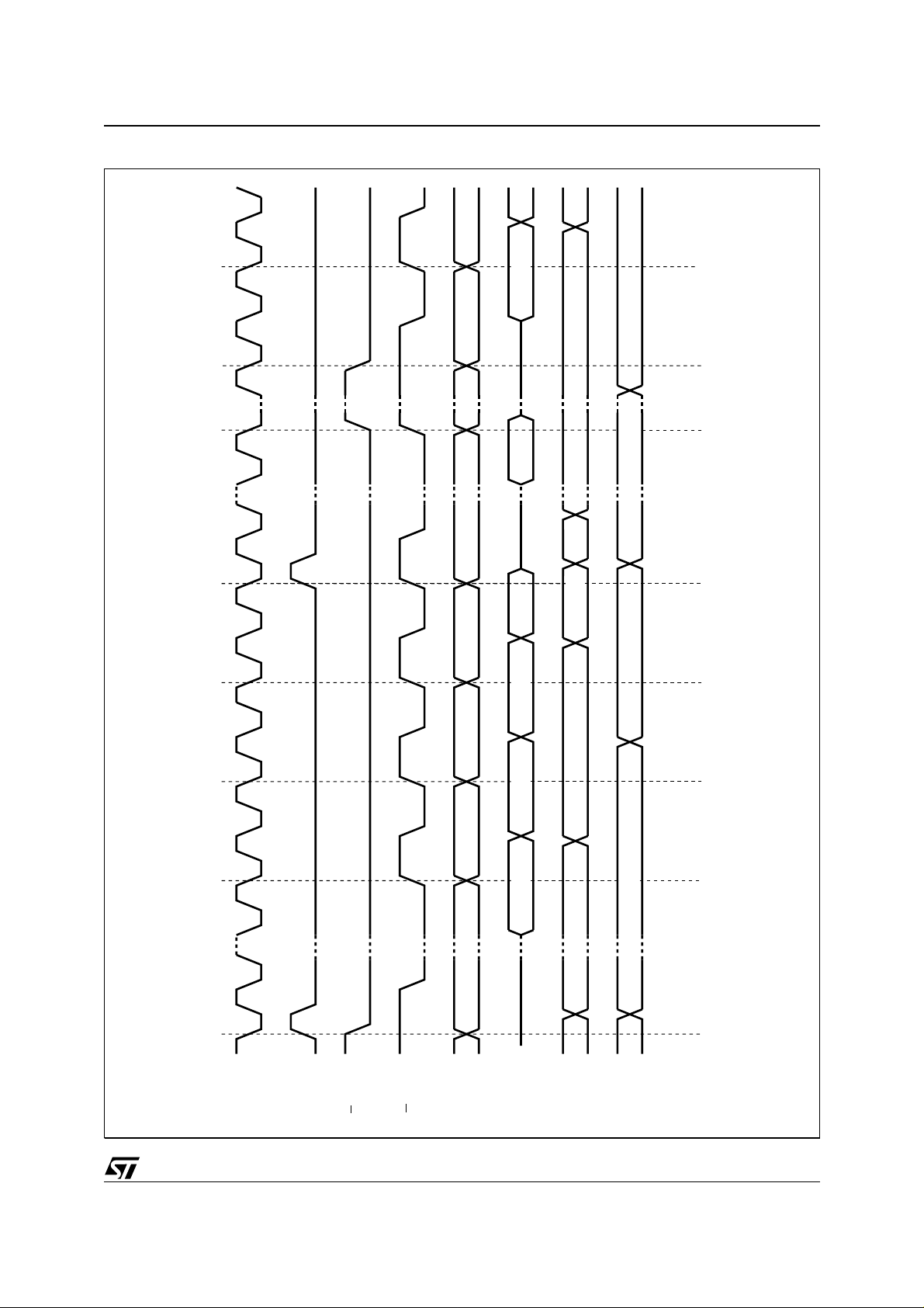
Figure 3. Non Linear and Linear Access Cycle Timing Diagram
M59BW102
OddEven
ADDR + 1 ADDR + 2
Odd
ADDRESS (Odd)ADDRESS (Even)
ADDR+3
ADDR + 2
RESUME
(LINEAR)
AI02766B
14 14
CLKOUT
ALE
E
G
ADDR + 1 ADDR + 2 ADDR + 3
A0-A15
EvenEven Odd Odd
DQ0-DQ15
ADDRESS (Even) ADDR + 2 ADDR + 4 ADDR + 1
Cntr even
ADDR + 1 ADDR + 3 ADDRESS (Odd)Cntr odd
NON LINEAR LINEAR LINEAR LINEAR NON LINEAR
5/24
M59BW102
Figure 4. Block Diagram
DQ0-DQ15
A1-A15
A0
G
LOGIC
E
ALE
EVEN COUNTER OUTPUT BUFFER ODD COUNTER
MULTIPLEXER
EVEN MATRIX
(16 x 32K)
ODD MATRIX
(16 x 32K)
INSTRUCTIONS AND COMMANDS
The Command Interface latches c ommands written to the memory. Instructions are made up from
one or more commands to perform Read Memory
Array, Read Electronic Signature, Program, Ch ip
Erase. Commands are made of address and data
sequences. The instructions require from 1 to 6 cycles, the first or first three of which are always write
operations used to initiate the instruction. They are
followed by either further write cycles to confirm
the first command or execute the command immediately. Command sequencing must be followed
exactly. Any invalid combination of commands will
reset the device to Read Array. The increased
number of cycles has been chosen to assure maximum data security. Instructions are initialised by
two initial Coded cycles which unlock the Command Interface. In addition, f or Erase, instruction
confirmation is again preceded by the two Co ded
cycles.
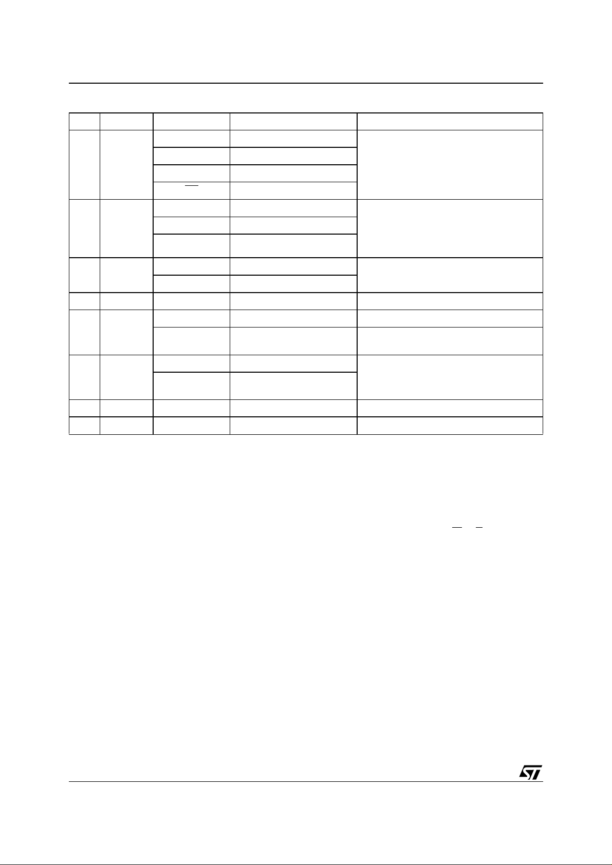
Status Register Bits
P/E.C. status is indicated during execution by Data
Polling on D Q7, detection of T oggle on DQ6 and
AI02765
DQ2, or Error on DQ5 and E ras e T imer DQ3 bits.
Any read attempt from any address during Program or Erase command execution will automatically output these five Status Register bits. The P/
E.C. automatically sets bits DQ2, DQ3, DQ5, DQ6
and DQ7. Other bits (DQ0, DQ1 and DQ4) are reserved for future use and should be masked. See
Table 8.
Data Polling Bit (DQ7). When Program ming operations are in progress, this bit out puts the complement of the bit being programmed on DQ7.
During Erase operation, it outputs a ’0’. After completion of the operation, DQ7 will output the bit last
program me d or a ’1 ’ after er asi ng. Data Pollin g is
valid and only effective during P/E.C. operation,
that is after the fourth W
after the six th W
pulse for erase. See Figure 11 for
pulse for programming or
the Data Polling waveforms and Figure 12 for the
Data Polling flowcha rt. A Valid Address is t he address being programmed or any address while
erasing the chip.
Toggle Bit (DQ6). When Programming or Erasing operations are in progress, successive attempts to read DQ6 will output complementary
6/24
M59BW102
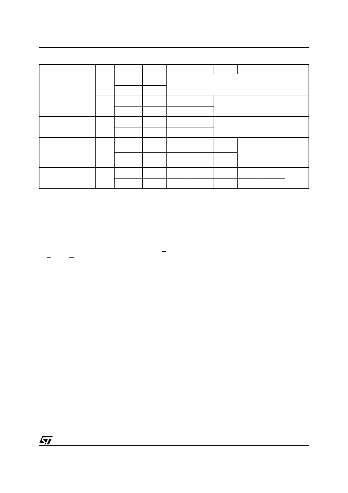
Table 7. Instructions
Mne. Instr . Cyc. 1st Cyc. 2nd Cyc. 3r d Cyc. 4th Cyc. 5th Cyc. 6th Cyc. 7th Cyc.
Read/Reset
(2,4)
RD
AS
Note: 1. Commands not interpreted in this table will default to read array mode.
Memor y Array
(4)
Auto Select 3+
PG Program 4
CE Chip Erase 6
2. A wait of 10µs is necessary after a Read/Reset command if the memory was in an Erase or Program mode before starting any new
operation.
3. X = Don't Care.
4. The f i rst cycles of the RD or AS instructions are followed by read operations. Any number of read cycles can occur after the command cycl e s.
5. Sig nat ure Addres s bits A0, A1, at V
code.
6. For C oded cycles address inputs A11-A16 are don't care.
7. Rea d Data Polling, Toggle bi ts until Erase comple t es.
(1)
1+
3+
(3,6)
Addr.
Data
(3,6)
Addr.
Data
(3,6)
Addr.
Data
(3,6)
Addr.
Data
(3,6)
Addr.
Data
will output Manufacturer code (20h). Address bits A0 at VIH and A1, at VIL will out put De vice
IL
X
Read Memory Array until a new write cycle is initiated.
F0h
555h 2AAh X
AAh 55h F0h
555h 2AAh 555h
AAh 55h 90h
555h 2AAh 555h
AAh 55h A0h
555h 2AAh 555h 555h 2AAh 555h
AAh 55h 80h AAh 55h 10h
Read Memory Array until a new write
cycle is initiated.
Read Electronic Signature until a new
write cycle is initiated. See Note 5.
Program
Address
Program
Data
Read Data Polling or Toggle
Bit until Program completes.
Note 7
data. DQ6 will toggle following toggling of either G,
or E
when G is low. The operation is completed
when two successive reads yield the same output
data. The next read will output the bit last programmed or a ’1’ after erasing. The toggle bit DQ6
is valid only during P/E.C. op erations, that is after
the fourth W
sixth W
pulse for programming or after the
pulse for Erase. See Figure 13 for Togg le
Bit flowchart and Figure 14 f or Toggle Bit waveforms .
Toggle Bit (DQ2). This toggle bit, together with
DQ6, can be used to det ermine the d evice status
during the Erase operations. During Chip Erase a
read operation will cause DQ2 to toggle since chip
is being erased. DQ2 will be set to ’1’ during program operation and when erase is complete.
Error Bit (DQ5). This bit is set to ’1’ by the P/E.C.
when there is a failure of programming or chip
erase that results in invalid data in the memory. In
case of an error in program, the ch ip must b e discarded. The DQ5 failure condition will also appear
if a user tries to program a ’1’ to a location that is
previously programmed to ’0’. The error bit resets
after a Read/Reset (RD) instruction. In case of
success of Pr ogram or Eras e, t he er ror b it w ill b e
set to ’0’.
Erase Timer Bit (DQ3). This bi t is s et to ’ 0’ by th e
P/E.C. when the Erase command has been entered to the Comm and Interface and it is awaiting
the Erase start. When the erase timeout period is
finished, after 50µs to 120µs, DQ3 returns to '1'.
Coded Cycles
The two Coded cycles unlock the Command Interface. They are followed by an input command or a
confirmation command. The Coded cycles consist
of writing the data AAh at address 555h during the
first cycle. During the second cycle the Coded cycles consist of writing the data 55h at address
2AAh. Address lines A0 to A10 are valid; other address lines are 'don't care'. The Coded cycl es happen on first and second cycles of the command
write or on the fourth and fifth cycles.
7/24
M59BW102
Table 8. Status Register Bits
DQ Name L ogic Level Defi nition Note
’1’ Erase Complete
Data
7
Polling
’0’ Erase On-going
DQ Program Complete
DQ
Program On-going
Indicates the P/E.C. status, check during
Program or Erase, and on completion before
checking bits DQ5 for Program or Erase
Success.
’-1-0-1-0-1-0-1-’ Erase or Program On-going Successive reads output complementary
6 Toggle Bit
5 Error Bit
4 Reserved
Erase
3
Time Bit
2 Toggle Bit
1 Reserved
0 Reserved
Note: Logic leve l ’1’ is High, ’0’ is Low. -0-1 -0-0-0-1-1-1-0- represent bit value in successive R ead operations.
Instructions
See Table 7.
Read/Reset (RD) Instruction. The Read/Reset
instruction consists of one write cycle giving the
command F0h. It can be optionally preceded by
the two Coded cycles. Subsequent read operations will r ead the memory array a ddressed and
output the data read. Read/Reset is not accepted
in Program/Erase operation unless a fail occurred.
Auto Select (AS) Instruction. This instruction
uses the two Coded cycles followed by one write
cycle giving the command 90h to address 555h for
command set-up. A subsequent read will output
the manufacturer code and the device code depending on the levels of A0 and A1. The manufacturer code, 20h, is output when the addresses
DQ Program Complete
’-1-1-1-1-1-1-1-’ Erase Complete
’1’ Program or Erase Error
’0’ Program or Erase On-going
’1’ Erase Timeout Period Expired P/E.C. Erase operation has started.
’0’
’-1-0-1-0-1-0-1-’ Chip Erase
’1’
Erase Timeout Period Ongoing
Program On-going or Erase
Complete
lines A0 and A1 are Low, t he de vice c ode, C1h is
output when A0 is High with A1 Low.
Program (PG) Instruction. This ins truction uses
four write cycles. The Program command A0h is
written to address 555h on the third cycle after two
Coded cycles. A fourth write operation latches the
Address on the falling edge of W
to be written on the rising edge and starts the P/
E.C. Read operations o utput the Status Register
bits after the programming has started. Memory
programming is made only by writing ’0’ in place of
’1’. Status bits DQ6 and DQ7 determine if programming is on-going and DQ5 allows verification
of any possible error.
Chip Erase (CE) Instructi on. This instruction uses
six write cycles. The Set-up command 80h is writ-
data on DQ6 while Programming or Erase
operations are on-going. DQ6 remains at
constant level when P/E.C. operations are
completed.
This bit is set to ’1’ in the case of
Programming or Erase failure.
Indicates the erase status.
or E and the Data
8/24
 Loading...